Consent Manager Tag v2.0 (for TCF 2.0) -->
Farnell PDF

 STM32F103x8 STM32F103xB - Farnell Element 14
STM32F103x8 STM32F103xB - Farnell Element 14
- Revenir à l'accueil


")

Farnell Element 14 :
![[TXT]](http://www.audentia-gestion.fr/icons/text.gif) Farnell-Full-Datashe..> 15-Jul-2014 17:08 951K
Farnell-Full-Datashe..> 15-Jul-2014 17:08 951K
Farnell-pmbta13_pmbt..> 15-Jul-2014 17:06 959K
Farnell-EE-SPX303N-4..> 15-Jul-2014 17:06 969K
Farnell-Datasheet-NX..> 15-Jul-2014 17:06 1.0M
Farnell-Datasheet-Fa..> 15-Jul-2014 17:05 1.0M
Farnell-MIDAS-un-tra..> 15-Jul-2014 17:05 1.0M
Farnell-SERIAL-TFT-M..> 15-Jul-2014 17:05 1.0M
Farnell-MCOC1-Farnel..> 15-Jul-2014 17:05 1.0M
Farnell-TMR-2-series..> 15-Jul-2014 16:48 787K
Farnell-DC-DC-Conver..> 15-Jul-2014 16:48 781K
Farnell-Full-Datashe..> 15-Jul-2014 16:47 803K
Farnell-TMLM-Series-..> 15-Jul-2014 16:47 810K
Farnell-TEL-5-Series..> 15-Jul-2014 16:47 814K
Farnell-TXL-series-t..> 15-Jul-2014 16:47 829K
Farnell-TEP-150WI-Se..> 15-Jul-2014 16:47 837K
Farnell-AC-DC-Power-..> 15-Jul-2014 16:47 845K
Farnell-TIS-Instruct..> 15-Jul-2014 16:47 845K
Farnell-TOS-tracopow..> 15-Jul-2014 16:47 852K
Farnell-TCL-DC-traco..> 15-Jul-2014 16:46 858K
Farnell-TIS-series-t..> 15-Jul-2014 16:46 875K
Farnell-TMR-2-Series..> 15-Jul-2014 16:46 897K
Farnell-TMR-3-WI-Ser..> 15-Jul-2014 16:46 939K
Farnell-TEN-8-WI-Ser..> 15-Jul-2014 16:46 939K
Farnell-Full-Datashe..> 15-Jul-2014 16:46 947K
Farnell-HIP4081A-Int..> 07-Jul-2014 19:47 1.0M
Farnell-ISL6251-ISL6..> 07-Jul-2014 19:47 1.1M
Farnell-DG411-DG412-..> 07-Jul-2014 19:47 1.0M
Farnell-3367-ARALDIT..> 07-Jul-2014 19:46 1.2M
Farnell-ICM7228-Inte..> 07-Jul-2014 19:46 1.1M
Farnell-Data-Sheet-K..> 07-Jul-2014 19:46 1.2M
Farnell-Silica-Gel-M..> 07-Jul-2014 19:46 1.2M
Farnell-TKC2-Dusters..> 07-Jul-2014 19:46 1.2M
Farnell-CRC-HANDCLEA..> 07-Jul-2014 19:46 1.2M
Farnell-760G-French-..> 07-Jul-2014 19:45 1.2M
Farnell-Decapant-KF-..> 07-Jul-2014 19:45 1.2M
Farnell-1734-ARALDIT..> 07-Jul-2014 19:45 1.2M
Farnell-Araldite-Fus..> 07-Jul-2014 19:45 1.2M
Farnell-fiche-de-don..> 07-Jul-2014 19:44 1.4M
Farnell-safety-data-..> 07-Jul-2014 19:44 1.4M
Farnell-A-4-Hardener..> 07-Jul-2014 19:44 1.4M
Farnell-CC-Debugger-..> 07-Jul-2014 19:44 1.5M
Farnell-MSP430-Hardw..> 07-Jul-2014 19:43 1.8M
Farnell-SmartRF06-Ev..> 07-Jul-2014 19:43 1.6M
Farnell-CC2531-USB-H..> 07-Jul-2014 19:43 1.8M
Farnell-Alimentation..> 07-Jul-2014 19:43 1.8M
Farnell-BK889B-PONT-..> 07-Jul-2014 19:42 1.8M
Farnell-User-Guide-M..> 07-Jul-2014 19:41 2.0M
Farnell-T672-3000-Se..> 07-Jul-2014 19:41 2.0M


See the trailer for the next exciting episode of The Ben Heck show. Check back on Friday to be among the first to see the exclusive full show on element…

Connect your Raspberry Pi to a breadboard, download some code and create a push-button audio play project.


Puce électronique / Microchip :


Sans fil - Wireless :


Texas instrument :


Ordinateurs :


Logiciels :


Tutoriels :


Autres documentations :
Farnell-0050375063-D..> 18-Jul-2014 17:03 2.5M
Farnell-Mini-Fit-Jr-..> 18-Jul-2014 17:03 2.5M
Farnell-43031-0002-M..> 18-Jul-2014 17:03 2.5M
Farnell-0433751001-D..> 18-Jul-2014 17:02 2.5M
Farnell-Cube-3D-Prin..> 18-Jul-2014 17:02 2.5M
Farnell-MTX-Compact-..> 18-Jul-2014 17:01 2.5M
Farnell-MTX-3250-MTX..> 18-Jul-2014 17:01 2.5M
Farnell-ATtiny26-L-A..> 18-Jul-2014 17:00 2.6M
Farnell-MCP3421-Micr..> 18-Jul-2014 17:00 1.2M
Farnell-LM19-Texas-I..> 18-Jul-2014 17:00 1.2M
Farnell-Data-Sheet-S..> 18-Jul-2014 17:00 1.2M
Farnell-LMH6518-Texa..> 18-Jul-2014 16:59 1.3M
Farnell-AD7719-Low-V..> 18-Jul-2014 16:59 1.4M
Farnell-DAC8143-Data..> 18-Jul-2014 16:59 1.5M
Farnell-BGA7124-400-..> 18-Jul-2014 16:59 1.5M
Farnell-SICK-OPTIC-E..> 18-Jul-2014 16:58 1.5M
Farnell-LT3757-Linea..> 18-Jul-2014 16:58 1.6M
Farnell-LT1961-Linea..> 18-Jul-2014 16:58 1.6M
Farnell-PIC18F2420-2..> 18-Jul-2014 16:57 2.5M
Farnell-DS3231-DS-PD..> 18-Jul-2014 16:57 2.5M
Farnell-RDS-80-PDF.htm 18-Jul-2014 16:57 1.3M
Farnell-AD8300-Data-..> 18-Jul-2014 16:56 1.3M
Farnell-LT6233-Linea..> 18-Jul-2014 16:56 1.3M
Farnell-MAX1365-MAX1..> 18-Jul-2014 16:56 1.4M
Farnell-XPSAF5130-PD..> 18-Jul-2014 16:56 1.4M
Farnell-DP83846A-DsP..> 18-Jul-2014 16:55 1.5M
Farnell-Dremel-Exper..> 18-Jul-2014 16:55 1.6M
Farnell-MCOC1-Farnel..> 16-Jul-2014 09:04 1.0M
Farnell-SL3S1203_121..> 16-Jul-2014 09:04 1.1M
Farnell-PN512-Full-N..> 16-Jul-2014 09:03 1.4M
Farnell-SL3S4011_402..> 16-Jul-2014 09:03 1.1M
Farnell-LPC408x-7x 3..> 16-Jul-2014 09:03 1.6M
Farnell-PCF8574-PCF8..> 16-Jul-2014 09:03 1.7M
Farnell-LPC81xM-32-b..> 16-Jul-2014 09:02 2.0M
Farnell-LPC1769-68-6..> 16-Jul-2014 09:02 1.9M
Farnell-Download-dat..> 16-Jul-2014 09:02 2.2M
Farnell-LPC3220-30-4..> 16-Jul-2014 09:02 2.2M
Farnell-LPC11U3x-32-..> 16-Jul-2014 09:01 2.4M
Farnell-SL3ICS1002-1..> 16-Jul-2014 09:01 2.5M
Farnell-T672-3000-Se..> 08-Jul-2014 18:59 2.0M
Farnell-tesa®pack63..> 08-Jul-2014 18:56 2.0M
Farnell-Encodeur-USB..> 08-Jul-2014 18:56 2.0M
Farnell-CC2530ZDK-Us..> 08-Jul-2014 18:55 2.1M
Farnell-2020-Manuel-..> 08-Jul-2014 18:55 2.1M
Farnell-Synchronous-..> 08-Jul-2014 18:54 2.1M
Farnell-Arithmetic-L..> 08-Jul-2014 18:54 2.1M
Farnell-NA555-NE555-..> 08-Jul-2014 18:53 2.2M
Farnell-4-Bit-Magnit..> 08-Jul-2014 18:53 2.2M
Farnell-LM555-Timer-..> 08-Jul-2014 18:53 2.2M
Farnell-L293d-Texas-..> 08-Jul-2014 18:53 2.2M
Farnell-SN54HC244-SN..> 08-Jul-2014 18:52 2.3M
Farnell-MAX232-MAX23..> 08-Jul-2014 18:52 2.3M
Farnell-High-precisi..> 08-Jul-2014 18:51 2.3M
Farnell-SMU-Instrume..> 08-Jul-2014 18:51 2.3M
Farnell-900-Series-B..> 08-Jul-2014 18:50 2.3M
Farnell-BA-Series-Oh..> 08-Jul-2014 18:50 2.3M
Farnell-UTS-Series-S..> 08-Jul-2014 18:49 2.5M
Farnell-270-Series-O..> 08-Jul-2014 18:49 2.3M
Farnell-UTS-Series-S..> 08-Jul-2014 18:49 2.8M
Farnell-Tiva-C-Serie..> 08-Jul-2014 18:49 2.6M
Farnell-UTO-Souriau-..> 08-Jul-2014 18:48 2.8M
Farnell-Clipper-Seri..> 08-Jul-2014 18:48 2.8M
Farnell-SOURIAU-Cont..> 08-Jul-2014 18:47 3.0M
Farnell-851-Series-P..> 08-Jul-2014 18:47 3.0M
Farnell-SL59830-Inte..> 06-Jul-2014 10:07 1.0M
Farnell-ALF1210-PDF.htm 06-Jul-2014 10:06 4.0M
Farnell-AD7171-16-Bi..> 06-Jul-2014 10:06 1.0M
Farnell-Low-Noise-24..> 06-Jul-2014 10:05 1.0M
Farnell-ESCON-Featur..> 06-Jul-2014 10:05 938K
Farnell-74LCX573-Fai..> 06-Jul-2014 10:05 1.9M
Farnell-1N4148WS-Fai..> 06-Jul-2014 10:04 1.9M
Farnell-FAN6756-Fair..> 06-Jul-2014 10:04 850K
Farnell-Datasheet-Fa..> 06-Jul-2014 10:04 861K
Farnell-ES1F-ES1J-fi..> 06-Jul-2014 10:04 867K
Farnell-QRE1113-Fair..> 06-Jul-2014 10:03 879K
Farnell-2N7002DW-Fai..> 06-Jul-2014 10:03 886K
Farnell-FDC2512-Fair..> 06-Jul-2014 10:03 886K
Farnell-FDV301N-Digi..> 06-Jul-2014 10:03 886K
Farnell-S1A-Fairchil..> 06-Jul-2014 10:03 896K
Farnell-BAV99-Fairch..> 06-Jul-2014 10:03 896K
Farnell-74AC00-74ACT..> 06-Jul-2014 10:03 911K
Farnell-NaPiOn-Panas..> 06-Jul-2014 10:02 911K
Farnell-LQ-RELAYS-AL..> 06-Jul-2014 10:02 924K
Farnell-ev-relays-ae..> 06-Jul-2014 10:02 926K
Farnell-ESCON-Featur..> 06-Jul-2014 10:02 931K
Farnell-Amplifier-In..> 06-Jul-2014 10:02 940K
Farnell-Serial-File-..> 06-Jul-2014 10:02 941K
Farnell-Both-the-Del..> 06-Jul-2014 10:01 948K
Farnell-Videk-PDF.htm 06-Jul-2014 10:01 948K
Farnell-EPCOS-173438..> 04-Jul-2014 10:43 3.3M
Farnell-Sensorless-C..> 04-Jul-2014 10:42 3.3M
Farnell-197.31-KB-Te..> 04-Jul-2014 10:42 3.3M
Farnell-PIC12F609-61..> 04-Jul-2014 10:41 3.7M
Farnell-PADO-semi-au..> 04-Jul-2014 10:41 3.7M
Farnell-03-iec-runds..> 04-Jul-2014 10:40 3.7M
Farnell-ACC-Silicone..> 04-Jul-2014 10:40 3.7M
Farnell-Series-TDS10..> 04-Jul-2014 10:39 4.0M
Farnell-03-iec-runds..> 04-Jul-2014 10:40 3.7M
Farnell-0430300011-D..> 14-Jun-2014 18:13 2.0M
Farnell-06-6544-8-PD..> 26-Mar-2014 17:56 2.7M
Farnell-3M-Polyimide..> 21-Mar-2014 08:09 3.9M
Farnell-3M-VolitionT..> 25-Mar-2014 08:18 3.3M
Farnell-10BQ060-PDF.htm 14-Jun-2014 09:50 2.4M
Farnell-10TPB47M-End..> 14-Jun-2014 18:16 3.4M
Farnell-12mm-Size-In..> 14-Jun-2014 09:50 2.4M
Farnell-24AA024-24LC..> 23-Jun-2014 10:26 3.1M
Farnell-50A-High-Pow..> 20-Mar-2014 17:31 2.9M
Farnell-197.31-KB-Te..> 04-Jul-2014 10:42 3.3M
Farnell-1907-2006-PD..> 26-Mar-2014 17:56 2.7M
Farnell-5910-PDF.htm 25-Mar-2014 08:15 3.0M
Farnell-6517b-Electr..> 29-Mar-2014 11:12 3.3M
Farnell-A-True-Syste..> 29-Mar-2014 11:13 3.3M
Farnell-ACC-Silicone..> 04-Jul-2014 10:40 3.7M
Farnell-AD524-PDF.htm 20-Mar-2014 17:33 2.8M
Farnell-ADL6507-PDF.htm 14-Jun-2014 18:19 3.4M
Farnell-ADSP-21362-A..> 20-Mar-2014 17:34 2.8M
Farnell-ALF1210-PDF.htm 04-Jul-2014 10:39 4.0M
Farnell-ALF1225-12-V..> 01-Apr-2014 07:40 3.4M
Farnell-ALF2412-24-V..> 01-Apr-2014 07:39 3.4M
Farnell-AN10361-Phil..> 23-Jun-2014 10:29 2.1M
Farnell-ARADUR-HY-13..> 26-Mar-2014 17:55 2.8M
Farnell-ARALDITE-201..> 21-Mar-2014 08:12 3.7M
Farnell-ARALDITE-CW-..> 26-Mar-2014 17:56 2.7M
Farnell-ATMEL-8-bit-..> 19-Mar-2014 18:04 2.1M
Farnell-ATMEL-8-bit-..> 11-Mar-2014 07:55 2.1M
Farnell-ATmega640-VA..> 14-Jun-2014 09:49 2.5M
Farnell-ATtiny20-PDF..> 25-Mar-2014 08:19 3.6M
Farnell-ATtiny26-L-A..> 13-Jun-2014 18:40 1.8M
Farnell-Alimentation..> 14-Jun-2014 18:24 2.5M
Farnell-Alimentation..> 01-Apr-2014 07:42 3.4M
Farnell-Amplificateu..> 29-Mar-2014 11:11 3.3M
Farnell-An-Improved-..> 14-Jun-2014 09:49 2.5M
Farnell-Atmel-ATmega..> 19-Mar-2014 18:03 2.2M
Farnell-Avvertenze-e..> 14-Jun-2014 18:20 3.3M
Farnell-BC846DS-NXP-..> 13-Jun-2014 18:42 1.6M
Farnell-BC847DS-NXP-..> 23-Jun-2014 10:24 3.3M
Farnell-BF545A-BF545..> 23-Jun-2014 10:28 2.1M
Farnell-BK2650A-BK26..> 29-Mar-2014 11:10 3.3M
Farnell-BT151-650R-N..> 13-Jun-2014 18:40 1.7M
Farnell-BTA204-800C-..> 13-Jun-2014 18:42 1.6M
Farnell-BUJD203AX-NX..> 13-Jun-2014 18:41 1.7M
Farnell-BYV29F-600-N..> 13-Jun-2014 18:42 1.6M
Farnell-BYV79E-serie..> 10-Mar-2014 16:19 1.6M
Farnell-BZX384-serie..> 23-Jun-2014 10:29 2.1M
Farnell-Battery-GBA-..> 14-Jun-2014 18:13 2.0M
Farnell-C.A-6150-C.A..> 14-Jun-2014 18:24 2.5M
Farnell-C.A 8332B-C...> 01-Apr-2014 07:40 3.4M
Farnell-CC2560-Bluet..> 29-Mar-2014 11:14 2.8M
Farnell-CD4536B-Type..> 14-Jun-2014 18:13 2.0M
Farnell-CIRRUS-LOGIC..> 10-Mar-2014 17:20 2.1M
Farnell-CS5532-34-BS..> 01-Apr-2014 07:39 3.5M
Farnell-Cannon-ZD-PD..> 11-Mar-2014 08:13 2.8M
Farnell-Ceramic-tran..> 14-Jun-2014 18:19 3.4M
Farnell-Circuit-Note..> 26-Mar-2014 18:00 2.8M
Farnell-Circuit-Note..> 26-Mar-2014 18:00 2.8M
Farnell-Cles-electro..> 21-Mar-2014 08:13 3.9M
Farnell-Conception-d..> 11-Mar-2014 07:49 2.4M
Farnell-Connectors-N..> 14-Jun-2014 18:12 2.1M
Farnell-Construction..> 14-Jun-2014 18:25 2.5M
Farnell-Controle-de-..> 11-Mar-2014 08:16 2.8M
Farnell-Cordless-dri..> 14-Jun-2014 18:13 2.0M
Farnell-Current-Tran..> 26-Mar-2014 17:58 2.7M
Farnell-Current-Tran..> 26-Mar-2014 17:58 2.7M
Farnell-Current-Tran..> 26-Mar-2014 17:59 2.7M
Farnell-Current-Tran..> 26-Mar-2014 17:59 2.7M
Farnell-DC-Fan-type-..> 14-Jun-2014 09:48 2.5M
Farnell-DC-Fan-type-..> 14-Jun-2014 09:51 1.8M
Farnell-Davum-TMC-PD..> 14-Jun-2014 18:27 2.4M
Farnell-De-la-puissa..> 29-Mar-2014 11:10 3.3M
Farnell-Directive-re..> 25-Mar-2014 08:16 3.0M
Farnell-Documentatio..> 14-Jun-2014 18:26 2.5M
Farnell-Download-dat..> 13-Jun-2014 18:40 1.8M
Farnell-ECO-Series-T..> 20-Mar-2014 08:14 2.5M
Farnell-ELMA-PDF.htm 29-Mar-2014 11:13 3.3M
Farnell-EMC1182-PDF.htm 25-Mar-2014 08:17 3.0M
Farnell-EPCOS-173438..> 04-Jul-2014 10:43 3.3M
Farnell-EPCOS-Sample..> 11-Mar-2014 07:53 2.2M
Farnell-ES2333-PDF.htm 11-Mar-2014 08:14 2.8M
Farnell-Ed.081002-DA..> 19-Mar-2014 18:02 2.5M
Farnell-F28069-Picco..> 14-Jun-2014 18:14 2.0M
Farnell-F42202-PDF.htm 19-Mar-2014 18:00 2.5M
Farnell-FDS-ITW-Spra..> 14-Jun-2014 18:22 3.3M
Farnell-FICHE-DE-DON..> 10-Mar-2014 16:17 1.6M
Farnell-Fastrack-Sup..> 23-Jun-2014 10:25 3.3M
Farnell-Ferric-Chlor..> 29-Mar-2014 11:14 2.8M
Farnell-Fiche-de-don..> 14-Jun-2014 09:47 2.5M
Farnell-Fiche-de-don..> 14-Jun-2014 18:26 2.5M
Farnell-Fluke-1730-E..> 14-Jun-2014 18:23 2.5M
Farnell-GALVA-A-FROI..> 26-Mar-2014 17:56 2.7M
Farnell-GALVA-MAT-Re..> 26-Mar-2014 17:57 2.7M
Farnell-GN-RELAYS-AG..> 20-Mar-2014 08:11 2.6M
Farnell-HC49-4H-Crys..> 14-Jun-2014 18:20 3.3M
Farnell-HFE1600-Data..> 14-Jun-2014 18:22 3.3M
Farnell-HI-70300-Sol..> 14-Jun-2014 18:27 2.4M
Farnell-HUNTSMAN-Adv..> 10-Mar-2014 16:17 1.7M
Farnell-Haute-vitess..> 11-Mar-2014 08:17 2.4M
Farnell-IP4252CZ16-8..> 13-Jun-2014 18:41 1.7M
Farnell-Instructions..> 19-Mar-2014 18:01 2.5M
Farnell-KSZ8851SNL-S..> 23-Jun-2014 10:28 2.1M
Farnell-L-efficacite..> 11-Mar-2014 07:52 2.3M
Farnell-LCW-CQ7P.CC-..> 25-Mar-2014 08:19 3.2M
Farnell-LME49725-Pow..> 14-Jun-2014 09:49 2.5M
Farnell-LOCTITE-542-..> 25-Mar-2014 08:15 3.0M
Farnell-LOCTITE-3463..> 25-Mar-2014 08:19 3.0M
Farnell-LUXEON-Guide..> 11-Mar-2014 07:52 2.3M
Farnell-Leaded-Trans..> 23-Jun-2014 10:26 3.2M
Farnell-Les-derniers..> 11-Mar-2014 07:50 2.3M
Farnell-Loctite3455-..> 25-Mar-2014 08:16 3.0M
Farnell-Low-cost-Enc..> 13-Jun-2014 18:42 1.7M
Farnell-Lubrifiant-a..> 26-Mar-2014 18:00 2.7M
Farnell-MC3510-PDF.htm 25-Mar-2014 08:17 3.0M
Farnell-MC21605-PDF.htm 11-Mar-2014 08:14 2.8M
Farnell-MCF532x-7x-E..> 29-Mar-2014 11:14 2.8M
Farnell-MICREL-KSZ88..> 11-Mar-2014 07:54 2.2M
Farnell-MICROCHIP-PI..> 19-Mar-2014 18:02 2.5M
Farnell-MOLEX-39-00-..> 10-Mar-2014 17:19 1.9M
Farnell-MOLEX-43020-..> 10-Mar-2014 17:21 1.9M
Farnell-MOLEX-43160-..> 10-Mar-2014 17:21 1.9M
Farnell-MOLEX-87439-..> 10-Mar-2014 17:21 1.9M
Farnell-MPXV7002-Rev..> 20-Mar-2014 17:33 2.8M
Farnell-MX670-MX675-..> 14-Jun-2014 09:46 2.5M
Farnell-Microchip-MC..> 13-Jun-2014 18:27 1.8M
Farnell-Microship-PI..> 11-Mar-2014 07:53 2.2M
Farnell-Midas-Active..> 14-Jun-2014 18:17 3.4M
Farnell-Midas-MCCOG4..> 14-Jun-2014 18:11 2.1M
Farnell-Miniature-Ci..> 26-Mar-2014 17:55 2.8M
Farnell-Mistral-PDF.htm 14-Jun-2014 18:12 2.1M
Farnell-Molex-83421-..> 14-Jun-2014 18:17 3.4M
Farnell-Molex-COMMER..> 14-Jun-2014 18:16 3.4M
Farnell-Molex-Crimp-..> 10-Mar-2014 16:27 1.7M
Farnell-Multi-Functi..> 20-Mar-2014 17:38 3.0M
Farnell-NTE_SEMICOND..> 11-Mar-2014 07:52 2.3M
Farnell-NXP-74VHC126..> 10-Mar-2014 16:17 1.6M
Farnell-NXP-BT136-60..> 11-Mar-2014 07:52 2.3M
Farnell-NXP-PBSS9110..> 10-Mar-2014 17:21 1.9M
Farnell-NXP-PCA9555 ..> 11-Mar-2014 07:54 2.2M
Farnell-NXP-PMBFJ620..> 10-Mar-2014 16:16 1.7M
Farnell-NXP-PSMN1R7-..> 10-Mar-2014 16:17 1.6M
Farnell-NXP-PSMN7R0-..> 10-Mar-2014 17:19 2.1M
Farnell-NXP-TEA1703T..> 11-Mar-2014 08:15 2.8M
Farnell-Nilï¬-sk-E-..> 14-Jun-2014 09:47 2.5M
Farnell-Novembre-201..> 20-Mar-2014 17:38 3.3M
Farnell-OMRON-Master..> 10-Mar-2014 16:26 1.8M
Farnell-OSLON-SSL-Ce..> 19-Mar-2014 18:03 2.1M
Farnell-OXPCIE958-FB..> 13-Jun-2014 18:40 1.8M
Farnell-PADO-semi-au..> 04-Jul-2014 10:41 3.7M
Farnell-PBSS5160T-60..> 19-Mar-2014 18:03 2.1M
Farnell-PDTA143X-ser..> 20-Mar-2014 08:12 2.6M
Farnell-PDTB123TT-NX..> 13-Jun-2014 18:43 1.5M
Farnell-PESD5V0F1BL-..> 13-Jun-2014 18:43 1.5M
Farnell-PESD9X5.0L-P..> 13-Jun-2014 18:43 1.6M
Farnell-PIC12F609-61..> 04-Jul-2014 10:41 3.7M
Farnell-PIC18F2455-2..> 23-Jun-2014 10:27 3.1M
Farnell-PIC24FJ256GB..> 14-Jun-2014 09:51 2.4M
Farnell-PMBT3906-PNP..> 13-Jun-2014 18:44 1.5M
Farnell-PMBT4403-PNP..> 23-Jun-2014 10:27 3.1M
Farnell-PMEG4002EL-N..> 14-Jun-2014 18:18 3.4M
Farnell-PMEG4010CEH-..> 13-Jun-2014 18:43 1.6M
Farnell-Panasonic-15..> 23-Jun-2014 10:29 2.1M
Farnell-Panasonic-EC..> 20-Mar-2014 17:36 2.6M
Farnell-Panasonic-EZ..> 20-Mar-2014 08:10 2.6M
Farnell-Panasonic-Id..> 20-Mar-2014 17:35 2.6M
Farnell-Panasonic-Ne..> 20-Mar-2014 17:36 2.6M
Farnell-Panasonic-Ra..> 20-Mar-2014 17:37 2.6M
Farnell-Panasonic-TS..> 20-Mar-2014 08:12 2.6M
Farnell-Panasonic-Y3..> 20-Mar-2014 08:11 2.6M
Farnell-Pico-Spox-Wi..> 10-Mar-2014 16:16 1.7M
Farnell-Pompes-Charg..> 24-Apr-2014 20:23 3.3M
Farnell-Ponts-RLC-po..> 14-Jun-2014 18:23 3.3M
Farnell-Portable-Ana..> 29-Mar-2014 11:16 2.8M
Farnell-Premier-Farn..> 21-Mar-2014 08:11 3.8M
Farnell-Produit-3430..> 14-Jun-2014 09:48 2.5M
Farnell-Proskit-SS-3..> 10-Mar-2014 16:26 1.8M
Farnell-Puissance-ut..> 11-Mar-2014 07:49 2.4M
Farnell-Q48-PDF.htm 23-Jun-2014 10:29 2.1M
Farnell-Radial-Lead-..> 20-Mar-2014 08:12 2.6M
Farnell-Realiser-un-..> 11-Mar-2014 07:51 2.3M
Farnell-Reglement-RE..> 21-Mar-2014 08:08 3.9M
Farnell-Repartiteurs..> 14-Jun-2014 18:26 2.5M
Farnell-S-TRI-SWT860..> 21-Mar-2014 08:11 3.8M
Farnell-SB175-Connec..> 11-Mar-2014 08:14 2.8M
Farnell-SMBJ-Transil..> 29-Mar-2014 11:12 3.3M
Farnell-SOT-23-Multi..> 11-Mar-2014 07:51 2.3M
Farnell-SPLC780A1-16..> 14-Jun-2014 18:25 2.5M
Farnell-SSC7102-Micr..> 23-Jun-2014 10:25 3.2M
Farnell-SVPE-series-..> 14-Jun-2014 18:15 2.0M
Farnell-Sensorless-C..> 04-Jul-2014 10:42 3.3M
Farnell-Septembre-20..> 20-Mar-2014 17:46 3.7M
Farnell-Serie-PicoSc..> 19-Mar-2014 18:01 2.5M
Farnell-Serie-Standa..> 14-Jun-2014 18:23 3.3M
Farnell-Series-2600B..> 20-Mar-2014 17:30 3.0M
Farnell-Series-TDS10..> 04-Jul-2014 10:39 4.0M
Farnell-Signal-PCB-R..> 14-Jun-2014 18:11 2.1M
Farnell-Strangkuhlko..> 21-Mar-2014 08:09 3.9M
Farnell-Supercapacit..> 26-Mar-2014 17:57 2.7M
Farnell-TDK-Lambda-H..> 14-Jun-2014 18:21 3.3M
Farnell-TEKTRONIX-DP..> 10-Mar-2014 17:20 2.0M
Farnell-Tektronix-AC..> 13-Jun-2014 18:44 1.5M
Farnell-Telemetres-l..> 20-Mar-2014 17:46 3.7M
Farnell-Termometros-..> 14-Jun-2014 18:14 2.0M
Farnell-The-essentia..> 10-Mar-2014 16:27 1.7M
Farnell-U2270B-PDF.htm 14-Jun-2014 18:15 3.4M
Farnell-USB-Buccanee..> 14-Jun-2014 09:48 2.5M
Farnell-USB1T11A-PDF..> 19-Mar-2014 18:03 2.1M
Farnell-V4N-PDF.htm 14-Jun-2014 18:11 2.1M
Farnell-WetTantalum-..> 11-Mar-2014 08:14 2.8M
Farnell-XPS-AC-Octop..> 14-Jun-2014 18:11 2.1M
Farnell-XPS-MC16-XPS..> 11-Mar-2014 08:15 2.8M
Farnell-YAGEO-DATA-S..> 11-Mar-2014 08:13 2.8M
Farnell-ZigBee-ou-le..> 11-Mar-2014 07:50 2.4M
Farnell-celpac-SUL84..> 21-Mar-2014 08:11 3.8M
Farnell-china_rohs_o..> 21-Mar-2014 10:04 3.9M
Farnell-cree-Xlamp-X..> 20-Mar-2014 17:34 2.8M
Farnell-cree-Xlamp-X..> 20-Mar-2014 17:35 2.7M
Farnell-cree-Xlamp-X..> 20-Mar-2014 17:31 2.9M
Farnell-cree-Xlamp-m..> 20-Mar-2014 17:32 2.9M
Farnell-cree-Xlamp-m..> 20-Mar-2014 17:32 2.9M
Farnell-ir1150s_fr.p..> 29-Mar-2014 11:11 3.3M
Farnell-manual-bus-p..> 10-Mar-2014 16:29 1.9M
Farnell-propose-plus..> 11-Mar-2014 08:19 2.8M
Farnell-techfirst_se..> 21-Mar-2014 08:08 3.9M
Farnell-testo-205-20..> 20-Mar-2014 17:37 3.0M
Farnell-testo-470-Fo..> 20-Mar-2014 17:38 3.0M
Farnell-uC-OS-III-Br..> 10-Mar-2014 17:20 2.0M
Sefram-7866HD.pdf-PD..> 29-Mar-2014 11:46 472K
Sefram-CAT_ENREGISTR..> 29-Mar-2014 11:46 461K
Sefram-CAT_MESUREURS..> 29-Mar-2014 11:46 435K
Sefram-GUIDE_SIMPLIF..> 29-Mar-2014 11:46 481K
Sefram-GUIDE_SIMPLIF..> 29-Mar-2014 11:46 442K
Sefram-GUIDE_SIMPLIF..> 29-Mar-2014 11:46 422K
Sefram-SP270.pdf-PDF..> 29-Mar-2014 11:46 464K
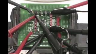
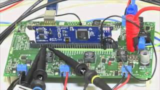
This is information on a product in full production.
August 2013 DocID13587 Rev 16 1/105
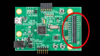
STM32F103x8
STM32F103xB
Medium-density performance line ARM-based 32-bit MCU with 64
or 128 KB Flash, USB, CAN, 7 timers, 2 ADCs, 9 com. interfaces
Datasheet - production data
Features
ARM 32-bit Cortex™-M3 CPU Core
– 72 MHz maximum frequency,
1.25 DMIPS/MHz (Dhrystone 2.1)
performance at 0 wait state memory
access
– Single-cycle multiplication and hardware
division
Memories
– 64 or 128 Kbytes of Flash memory
– 20 Kbytes of SRAM
Clock, reset and supply management
– 2.0 to 3.6 V application supply and I/Os
– POR, PDR, and programmable voltage
detector (PVD)
– 4-to-16 MHz crystal oscillator
– Internal 8 MHz factory-trimmed RC
– Internal 40 kHz RC
– PLL for CPU clock
– 32 kHz oscillator for RTC with calibration
Low power
– Sleep, Stop and Standby modes
– VBAT supply for RTC and backup registers
2 x 12-bit, 1 μs A/D converters (up to 16
channels)
– Conversion range: 0 to 3.6 V
– Dual-sample and hold capability
– Temperature sensor
DMA
– 7-channel DMA controller
– Peripherals supported: timers, ADC, SPIs,
I2Cs and USARTs
Up to 80 fast I/O ports
– 26/37/51/80 I/Os, all mappable on 16
external interrupt vectors and almost all
5 V-tolerant
Debug mode
– Serial wire debug (SWD) & JTAG
interfaces
7 timers
– Three 16-bit timers, each with up to 4
IC/OC/PWM or pulse counter and
quadrature (incremental) encoder input
– 16-bit, motor control PWM timer with deadtime
generation and emergency stop
– 2 watchdog timers (Independent and
Window)
– SysTick timer 24-bit downcounter
Up to 9 communication interfaces
– Up to 2 x I2C interfaces (SMBus/PMBus)
– Up to 3 USARTs (ISO 7816 interface, LIN,
IrDA capability, modem control)
– Up to 2 SPIs (18 Mbit/s)
– CAN interface (2.0B Active)
– USB 2.0 full-speed interface
CRC calculation unit, 96-bit unique ID
Packages are ECOPACK®
Table 1. Device summary
Reference Part number
STM32F103x8 STM32F103C8, STM32F103R8
STM32F103V8, STM32F103T8
STM32F103xB STM32F103RB STM32F103VB,
STM32F103CB, STM32F103TB
BGA100 10 × 10 mm
UFBGA100 7 x 7 mm
BGA64 5 × 5 mm
VFQFPN36 6 × 6 mm
LQFP100 14 × 14 mm
LQFP64 10 × 10 mm
LQFP48 7 × 7 mm
UFQFPN48 7 × 7 mm
www.st.com
2012-2013
Dremel Experts: US: 1 (800) 437-3635 Canada: 1 (888) 285-3476 www.dremel.com
The M akers o f Scan this code with your phone for
product information, videos, and more.
Do you like to:
REA D
Visit Dremel.com and get tips and tricks on projects and
products. Plus visit our message board or sign up for our
monthly eblast for news on new product introductions.
TALK
Join the conversation on Facebook
at facebook.com/Dremel.
BE INSPIRE D
Sign up for weekly project inspiration
at DremelWeekends.com.
SHARE
Pin Dremel projects and ideas on Pinterest.
STAY UP-TO-DATE
Get the latest news from Dremel. Follow
us on Twitter, username @Dremel.
ROTARY TOOLS
Corded.. . . . . . . . . . . . . . . . . . . . . . . . . . . 1-12
Cordless.. . . . . . . . . . . . . . . . . . . . . . . 13-20
At tachments.. . . . . . . . . . . . . . . . . 21-26
Accessories.. . . . . . . . . . . . . . . . . . 27-42
OSCILLATING TOOLS
Mul t i-Max™ Corded.. . . . . . 43-48
Mul t i-Max™ Cordless.. . . . 49-50
Accessories.. . . . . . . . . . . . . . . . . . 51-54
At tachments.. . . . . . . . . . . . . . . . . . . . . 54
SPECIALTY TOOLS
Saw-Max™ System. . . . . . . . 55-60
Trio™ System.. . . . . . . . . . . . . . . . 61-66
VersaTip™ and
Accessories.. . . . . . . . . . . . . . . . . . . . . . 67
Engraver and
Accessories.. . . . . . . . . . . . . . . . . . . . . . 67
V ersatile Tool Systems™
INDEX
Customer
Support
A well-prepared staff of
Dremel Experts is available to
answer questions about our tools.
With over 650 total years of
combined work experience, the
Dremel Experts are ready to serve
you. Call:
1-800-4-DREMEL
(1-800-437-3635) USA.
1-888-285-3476 CANADA.
Cal l for Your
Free Dremel DVD
1(800) 437-3635
1
The Makers of Versatile
Tool Systems™
ROTARY TOOLS
2
What Is a Rotary Tool ?
Rotary tools are hand held power tools that use high-speed
and low torque to undertake a variety of useful tasks with
control and precision. Since AJ Dremel invented the first
rotary tool over 80 years ago, no other brand has worked
harder to bring users a more complete and innovative
system of rotary tools, accessories and attachments.
Over the years Dremel rotary tools have become the gold
standard in versatility, performance, and quality by which
all other rotary tools are judged.
3
4200, 4000,
8220
3000, 8100
ROTARY TOOL OVERVIEW CORDED
VERSATILITY METER
Model 4200 4000 3000 200
SERIES
100
SERIES
Amps 1.6 1.6 1.2 1.15 1.15
Speed Range
[RPM]
5,000—
35,000
5,000—
35,000
5,000—
32,000
15,000 and
35,000 35,000
Versatility Level High High Intermediate Basic + Basic
Electronic
Feedback Control Yes Yes No No No
Number of
Speeds Variable Variable Variable 2 1
Soft Grip Yes Yes Yes No No
Separate On/Off
Speed Control Yes Yes No No No
Accessory
Change System EZ Change™
EZ Twist™
Nose Cap
EZ Twist™
Nose Cap Wrench Wrench
Weight [oz.] 25 22.5 20.0 18.0 18.0
Warranty 2 year 2 year 2 year 2 year 2 year
High Intermediate
Models: Models:
Premium Rotary Tools, able t o
perform the wide st range o f
applications.
High Performance Rotary Tools,
able to tackle a wider r ange of
applications.
4
200 SERIES,
STYLUS, 7700
100 SERIES,
7300
ROTARY TOOL OVERVIEW CORDLESS
Model 8220 8100 STYLUS™ 7700 7300
Voltage 12Vmax 8Vmax 7.2 7.2 4.8
Battery
Type
Lithium
Ion
Lithium
Ion
Lithium
Ion Ni-Cd Ni-Cd
Speed Range
[RPM]
5,000—
30,000
5,000—
30,000
5,000—
25,000
10,000 and
20,000
6,500 and
13,000
Versatility Level High Intermediate Basic + Basic + Basic
Electronic
Feedback Control No No No No No
Number of
Speeds Variable Variable Variable 2 2
Soft Grip Yes Yes Yes No No
Separate On/Off
Speed Control Yes Yes Yes No No
Accessory
Change System
EZ Twist™
Nose Cap
EZ Twist™
Nose Cap Wrench Wrench Wrench
Weight [oz.] 22.0 14.0 9.0 12.0 9.0
Warranty 2 year 2 year 2 year 2 year 2 year
Basic + Basic
Models: Models:
Enhanced Level Rotary Tools,
with improved control across
multiple applications.
Entry Level Rotary Tools,
ideal for precision applications.
5
1 2 3
NEW!
PULL INSERT SECURE
Integrated EZ Change™
For the fastest and easiest
accessory change.
Patented pull
lever system
Means you'll never need to
look for the wrench again.
Variable Speed
For maximum accessory
versatility and precise
tool control.
Electronic Feedback
Auto adjusts power and
speed as needed.
Can be used with all
Dremel accessories
and attachments
except MS400 and
PL400 attachments.*
High-Performance Motor
For maximum
performance at
all speeds.
Separate On/Off Switch
Retains speed setting for
ease of use.
Increased power
and air flow
For cooler operation.
Limited
Warranty
CORDED ROTARY TOOLS
Versatility
* Attachment models 225, 575 and 670 are compatible
with the 4200 when used with the 4200 Attachment
Adapter found in your Dremel 4200 kit.
6
EZC480 EZC481 EZC482 EZC483
• 4200 High Performance Rotary Tool, Circle
Cutter, Safety Shield, Cutting Guide, Lawn
Mower Sharpener, Lawn Mower and Garden
Tool Sharpener, Sanding/Grinding Guide,
Detailers Grip
• Storage Case, Accessory Case, Product
Reference Sheet, Adapter/Drive Coupling
40 ASSORTED ACCESSORIES
Carving/Engraving - 107, 191
Grinding/Sharpening - 932, 8193, 84922
Cutting - EZ409, EZ456, 561
Cleaning/Polishing - 403, 428
Sanding - EZ407, 408 (x6), EZ411 (x3) EZ412 (x3), EZ413 (x3), 432 (x6), 445 (x6)
Miscellaneous - 150, EZ402
4200 KIT 4200 - 6/40
The following 4200-specific collets
are available for purchase. Call
1-800-4-DREMEL for more information.
2615001034 – EZC480
2615001035 – EZC481
2615001036 – EZC482
2615001037 – EZC483
1/8" 3/32" 1/16" 1/32"
3,2 mm 2,4 mm 1,6 mm 0,8 mm
4200 COLLETS
7
Electronic Feedback
Auto adjusts power and
speed as needed.
EZ Twist™
Nose Cap Wrench for fast
accessory changes.
Variable Speed
For maximum accessory
versatility and precise
tool control.
Can be used with all
Dremel accessories
and attachments.
Does it All, Better.™
Limited
Warranty Versatility
CORDED ROTARY TOOLS
High-Performance Motor
For maximum
performance at
all speeds.
Separate On/Off Switch
Retains speed setting for
ease of use.
360º Grip Zone
With soft grip for comfort
and control.
Quick Collet Lock
For fast accessory
changes.
Integrated nose cap
wrench for fast
accessory changes.
8
• 4000 High Performance Rotary Tool, Planer, Flex
Shaft, Circle Cutter, Sanding/Grinding Guide,
Cutting Guide, Detail Nose Piece, Lawn Mower
and Garden Tool Sharpener
• Storage Case, Accessory Case,
Product Reference Sheet, Wrench, 1/8" Collet
• 4000 High Performance Rotary Tool, Detailer’s
Grip, Sanding/Grinding Guide, Cutting Guide,
Circle Cutter
• Storage Case, Accessory Case,
Product Reference Sheet, Wrench, 1/8" Collet
• 4000 High Performance Rotary Tool, Sanding/
Grinding Guide, Circle Cutter
• Storage Case, Accessory Case,
Product Reference Sheet, Wrench, 1/8" Collet
Carving/Engraving - 107, 191, 194
Grinding/Sharpening - 541, 932, 8193, 84922
Cutting - 420 (x4), 540, 561, EZ409, EZ456 (x2), EZ476 (x2)
Cleaning/Polishing - 405, 414 (x3), 421, 428, 429, 442, EZ423
Sanding - 407, 408 (x2), 411 (x2), 412 (x2), 413 (x2), 432 (x2), 445 (x2), EZ511, EZ512
Miscellaneous - 150, 401, 402, 481, EZ402
50 ASSORTED ACCESSORIES
Carving/Engraving - 107, 191
Grinding/Sharpening - 932, 8193, 84922, 85602
Cutting - 420 (x2), 540, 561, EZ456
Cleaning/Polishing - 403, 414 (x3), 421, 428, 429 (x2), 802
Sanding - 407, 408, 411 (x2), 412, 413, 432 (x3), 445 (x2)
Miscellaneous - 401, 402, 481, EZ402
34 ASSORTED ACCESSORIES
Carving/Engraving - 191
Grinding/Sharpening - 541, 932, 84922
Cutting - 420 (x2), 426 (x2), 561
Cleaning/Polishing - 403, 414, 421, 428, 429
Sanding - 407, 408 (x3), 411 (x3), 412 (x2), 413 (x2), 432 (x2), 445 (x2)
Miscellaneous - 401, 402
30 ASSORTED ACCESSORIES
4000 KIT 4000 - 6/50
4000 KIT 4000 - 4/34
4000 KIT 4000 - 2/30
9
Versatility
Does it Better.™
CORDED ROTARY TOOLS
Limited
Warranty
EZ Twist™
Nose Cap Wrench for fast
accessory changes.
Variable Speed
For maximum accessory
versatility and precise
tool control.
Sealed Ball
Bearing Motor
Runs cool for comfort
and longer tool life.
Can be used with all
Dremel accessories
and attachments
except MS400 and
PL400 attachments.
Separate On/Off Switch
Retains speed setting
for ease of use.
Double hull construction
Eliminates direct heat
transfer to hand.
10
• 3000 Series Variable Speed Rotary Tool,
Sanding/Grinding Guide
• Storage Case, Accessory Case,
Product Reference Sheet
• Wrench, 1/8" Collet
• 3000 Series Variable Speed Rotary Tool,
Cutting Guide
• Storage Case, Accessory Case, Product
Reference Sheet
• Wrench, 1/8" Collet
Carving/Engraving - 191
Grinding/Sharpening - 932, 952, 85422
Cutting - 426 (x2)
Cleaning/Polishing - 403, 414 (x2), 421, 428, 429
Sanding - 407, 408, 430, 432 (x2), 438, 445 (x2), 446
Miscellaneous - 401, 402, 415
24 ASSORTED ACCESSORIES
Carving/Engraving - 107, 191, 7144
Grinding/Sharpening - 932, 952, 953, 84922
Cutting - 426 (x2), 560, 561
Cleaning/Polishing - 403, 404, 405, 414 (x2), 421, 428, 429 (x2)
Sanding - 407, 408 (x2), 432 (x2), 445 (x2)
Miscellaneous - 150, 401, 402, 415
31 ASSORTED ACCESSORIES
3000 KIT 3000 - 1/24
3000 KIT 3000 - 1/31
11
Versatility
Limited
Warranty
Two Speed control
For application versatility and control.
Sealed Ball Bearing Motor
For cool running and longer tool life.
• Two-Speed Rotary Tool, Lawn
Mower and Garden
Tool Sharpener
• Corrugated Storage Case,
Product Reference Sheet
• Wrench, 1/8" Collet
Carving/Engraving - 194
Grinding/Sharpening - 932, 8193, 83322
Cutting - 420, 426
Cleaning/Polishing - 421, 422, 425, 429
Sanding - 407, 408, 432
Miscellaneous - 401, 402
15 ASSORTED ACCESSORIES
• Two-Speed Rotary Tool, Cutting Guide
• Corrugated Storage Case,
Product Reference Sheet
• Wrench, 1/8" Collet
CORDED ROTARY TOOLS
200 SERIES KIT 200 - 1/15
200 SERIES KIT 200 - 1/21
Carving/Engraving - 194
Grinding/Sharpening - 932, 8193, 83142, 84922
Cutting - 420, 426, 561
Cleaning/Polishing - 414 (x2), 421, 422, 425 (x2), 429 (x2)
Sanding - 407, 432, 445
Miscellaneous - 401, 402, 415
21 ASSORTED ACCESSORIES
12
Single Speed control
For fulltime 35,000 rpm operation.
Sealed Ball Bearing Motor
For cool running and longer tool life.
Limited
Warranty
Ideal for sanding, carving
and drilling.
• Single-Speed Rotary Tool
• Product Reference Sheet
• Wrench, 1/8" Collet
100 SERIES KIT 100 - N/7
Versatility
Grinding/Sharpening - 932, 84922
Cutting - 420
Sanding - 407, 432
Miscellaneous - 402, 415
7 ASSORTED ACCESSORIES
13
Limited
Warranty
CORDLESS ROTARY TOOLS
Does it All, Unplugged.™
Next Generation 12V Max
For maximum performance
and run time.
Removable
Lithium-Ion Battery
Always ready with no
memory effects.
EZ Twist™
Nose Cap Wrench for fast
accessory changes.
Variable Speed
For maximum accessory
versatility and precise
tool control.
Versatility
High-Performance Motor
For maximum
performance at all speeds.
Can be used with all
Dremel accessories
and attachments.
Separate On/Off Switch
Retains speed setting for
ease of use.
360º Grip Zone
With soft grip for comfort
and control.
NEW!
NEW!
LITHIUM-ION TECHNOLOGY
• More power in a smaller size
• Always ready – holds charge up to 2 years
• No memory effects – charge any time
* When compared to 8200 while cutting screws
14
B812-01 876
12VMAX Lithium-Ion
Battery Pack
12VMAX 1-Hour
Lithium-Ion
Battery Charger
• 8220 Cordless 12VMAX High Performance
Rotary Tool, Cutting Guide
• 1-Hour Battery Charger,
12VMAX Lithium-Ion Battery Pack (1)
• Storage Case, Accessory Case,
Product Reference Sheet
• Wrench, 1/8" Collet
Grinding/Sharpening - 541, 8193
Cutting - 426, 561
Cleaning/Polishing - 414 (X4), 421, 425 (X4), 429 (X4)
Sanding - 407, 408 (X2), 432 (X3), 445 (X3)
Miscellaneous - 401, 402,
28 ASSORTED ACCESSORIES
• 8220 Cordless 12VMAX High Performance
Rotary Tool, Shield, Cutting Guide
• 1-Hour Battery Charger,
12VMAX Lithium-Ion Battery Packs (2)
• Storage Case, Accessory Case,
Product Reference Sheet
• Wrench, 1/8" Collet
Grinding/Sharpening - 541, 8193
Cutting - 561, 426, EZ456
Cleaning/Polishing - 414 (X3), 421, 425 (x4), 429 (x3)
Sanding - 407, 408 (X2), 432 (X3), 445 (X3)
Miscellaneous - 401, 402, EZ402
28 ASSORTED ACCESSORIES
Includes
2 batteries
8220 KIT 8220 - 1/28
8220 KIT 8220 - 2/28
CORDLESS 12VMAX ROTARY TOOL ACCESSORIES
15
Limited
Warranty
Versatility
CORDLESS ROTARY TOOLS
NEW!
EZ Twist™
Nose Cap Wrench for fast accessory changes.
Variable Speed
For maximum accessory versatility and precise
tool control.
8V Max Lithium-ion
For power in a smaller size, always ready
and no memory effects.
Can be used with all Dremel accessories
and attachments except MS400 and PL400
attachments.
Separate On/Off Switch
Retains speed setting for ease of use.
Small and Lightweight
For easier handling and less fatigue.
16
B808-01 876
• 8100 Cordless 8VMAX Rotary Tool
• 1-Hour Charger, 8VMAX Lithium-Ion Battery Pack (1)
• Compact Storage Case
• Wrench, 1/8" Collet
Grinding/Sharpening - 84922, 932, 952
Cutting - 540 (x3)
Cleaning/Polishing - 403, 414 (x2), 421
Sanding - 407, 408 (x3), 432 (x3), 445 (x2)
Miscellaneous - 401, 402
21 ASSORTED ACCESSORIES
8100 KIT 8100-N/21
CORDLESS 8VMAX ROTARY TOOL ACCESSORIES
8VMAX Lithium-Ion
Battery Pack
8VMAX 1-Hour
Lithium-Ion
Battery Charger
17
Limited
Warranty
Versatility
Variable Speed
For maximum accessory versatility
and precise tool control.
Rechargeable 7.2V Lithium-ion
Battery holds a charge 2 years while
in storage.
Unique Contoured Grip
Designed for superior precision,
control, and comfort in your hand.
Finger-Tip On/Off Switch
For one-handed operation.
Compact and Ultra-Lightweight
Can be used with most Dremel
accessories and no attachments.
Docking Station
Continually charges so the tool is
always fully charged and ready to use.
CORDLESS ROTARY TOOLS
• Always Ready
• Goes Everywhere
Created to Fit Your Hand
and Your Lifestyle™
18
• Dremel Stylus Rotary Tool
• Charging Base and Accessory Organizer
• Accessory Case, Product Reference Sheet
• Wrench, 1/8" Collet
Carving/Engraving - 105, 107, 191, 194
Grinding/Sharpening - 932, 84922
Cleaning/Polishing - 403, 414 (X4), 421, 425, 429 (X3)
Sanding - 430, 431, 438 (X2), 446, 521E
Miscellaneous - 401, 402, 481
25 ASSORTED ACCESSORIES
STYLUS KIT 1100 - N/25
19
757-01 758-01
Two Speeds
For control and accuracy.
Removable battery pack
Continuous use to finish your projects.
7.2 Volts of Power
. . . goes anywhere.
Light and Compact
Easy to handle and fun to use — anywhere!
3-Hour Charger
Quick battery recharge with LED light. Light
indicates battery is correctly placed into the
charger for proper charging.
Versatility Limited
Warranty
CORDLESS ROTARY TOOLS
3-Hour Battery
Charger
7.2V Battery Pack
7700 ACCESSORIES
• 7.2V Two-Speed Cordless Rotary Tool, Lawn
Mower and Garden Tool Sharpener
• Corrugated Storage Case, Accessory Organizer,
Product Reference Sheet
• 3-Hour Charger
• Wrench, 1/8" Collet
Carving/Engraving - 191
Grinding/Sharpening - 932, 8193, 83322
Cutting - 420, 426
Cleaning/Polishing - 421, 422, 425, 429
Sanding - 407, 408, 432
Miscellaneous - 401, 402
15 ASSORTED ACCESSORIES
7700 KIT 7700-02
20
755-01 756-01
Two Speeds
For control and accuracy.
Removable battery pack
Continuous use to finish your projects.
4.8 Volts of Power
For light duty precision jobs.
Light and Compact
Easy to handle and fun to use — anywhere!
3-Hour Charger
Quick battery recharge with LED light. Light
indicates battery is correctly placed into the
charger for proper charging.
Versatility Limited
Warranty
4.8V Battery Pack
7300 ACCESSORIES
• 4.8V Two-Speed MINIMITE®
• 3-Hour Charger
• Wrench, 1/8" Collet
Grinding/Sharpening - 84922
Cleaning/Polishing - 414
Sanding - 407, 432
Miscellaneous - 401
5 ASSORTED ACCESSORIES
3-Hour Battery
Charger
7300 KIT 750-02
21
220
225
231
335
565
566
568
575
A576
A577
670
675
678-01
1453
2500-01
A550
A679-02
4200 • * • • • • • • * • • * • • • • •
4000 • • • • • • • • • • • • • • • • •
400 • • • • • • • • • • • • • • • • •
3000 • • • • • • • • • • • • • • • • •
300 • • • • • • • • • • • • • • • • •
398 • • • • • • • • • • • • • • • • •
395 • • • • • • • • • • • • • • • • •
285 • • • • • • • • • • • • • • • • •
275 • • • • • • • • • • • • • • • •
200 • • • • • • • • • • • • • • • • •
100 • • • • • • • • • • • • • • • •
8220 • • • • • • • • • • • • • • • • •
8200 • • • • • • • • • • • • • • • • •
8100 • • • • • • • • • • • • • • •
800 • • • • • • • • • • • • • • •
770 • • • • •
750
1100
7300
ROTARY TOOL ATTACHMENT COMPATIBILITY KEY
SHIELD KIT MODEL A550
Increased comfort from debris and sparks
during cutting, grinding, sanding, and
polishing applications.
• Easy to Use – Spring friction design allows for
quick adjustment and accessibility to accessory.
• Compact for greater maneuverability.
Use this chart to find out which attachments work with your tool.
Adapters may be needed.
* This attachment is compatible with the 4200 when used with
the 4200 Attachment Adapter found in your Dremel 4200 kit.
Grinding/Sharpening - 8193
Cutting - EZ456
4 ASSORTED ACCESSORIES
ROTARY TOOL ATTACHMENTS
CORDLESS CORDED
ATTACHMENT MODEL NUMBER
Cleaning/Polishing - 428
Miscellaneous - EZ402
TOOL MODEL
NUMBER
22
107 481
Functions as an articulating drill press
that rotates 90º, rotary tool holder, and
flex-shaft tool stand.
• Detents click the tool in place in 15º
increments from vertical to horizontal.
• “Crow’s Nest” provides on-board
storage for Dremel accessories.
• Durable, die-cast aluminum base.
WORK STATION™ MODEL 220 - 01
Ideal for hard to reach places and fine detail work.
• Quick connect attach system.
• 36" long cable with new 5" bend radius
provides more flexibility.
• Comfort grip hand piece.
• Integrated shaft lock button.
• Holds up to 1/8" shank.
• Works with collet system and Dremel chuck.
FLEX SHAFT ATTACHMENT MODEL 225 - 01
TOOLS NOT INCLUDED WITH ATTACHMENTS
Transfers the weight of the tool to the palm of your
hand for improved tool balance and control.
• Offers enhanced grip and comfort for
detailed applications.
• Provides optimal tool control when precision
is required.
• Attaches onto a rotary tool in place of its nose piece
for quick and easy installation.
• Includes 107 engraving cutter and
tracing stencil.
DETAILER'S GRIP MODEL A577
23
• Allows for sturdy controlled cuts with
maximum visibility.
• Easy depth adjustment. Set to the correct cutting
depth for the material you are working on.
• Includes cutting guide, 2 drywall cutting bits for
cutting drywall for electrical boxes & air vents.
• Includes 1 multipurpose cutting bit for making cuts
in ceiling tile, wood, plastic, fiberglass, drywall,
laminate and vinyl siding.
MULTIPURPOSE CUTTING KIT MODEL 565
Converts your corded Rotary Tool into a bench
mounted wood shaper.
• Features an adjustable fence and large
8" x 6" worktable.
• Slot, groove, sand and trim edges.
SHAPER/ROUTER TABLE MODEL 231
Converts your corded Rotary Tool into a plunge router.
• Clear base.
• Two depth stops.
• Includes edge guide and circle guide.
• Rout circles, parallel to edge, signs and inlay
work and decorative edges.
PLUNGE ROUTER ATTACHMENT MODEL 335 - 01
Gets a Grip on Anything, Anywhere!
• Portable vise holds work piece for projects
such as woodworking, home projects, crafts
and hobbies.
• Clamps to any work surface up to 2-1/2" thick.
• Rotates 360º and tilts 50º allowing user to
lock the workpiece in any position.
• Tool holder turns Dremel Rotary Tools into a
stationary sander, grinder or polisher.
• Removable clamping jaws creates a stand-alone
bar clamp.
MULTI-VISE™ MODEL 2500 - 01
24
569
570
• Allows for sturdy controlled cuts with
maximum visibility.
• Easy depth adjustment. Set to the correct
cutting depth for the material you are working on.
• Includes cutting guide and tile cutting bit.
• Shape ceramic wall tile around fixtures or
plumbing pipes.
Not for use on ceramic floor tile.
• Also available: Model 570 1/8" Grout Removal Bit
(Not included with 568).
For use on wall and floor grout!
• Multiple slide depth adjustment.
• 30° angle for controlled cutting.
• Guides 180° apart to keep bit centered
between tiles.
• Easy screw-on mounting.
• Excellent cutting visibility.
• Includes 1/16" Grout Removal Bit – Model 569.
Made of solid carbide, the bit will remove both wall
and floor grout.
TILE CUTTING KIT MODEL 566
GROUT REMOVAL ATTACHMENT MODEL 568
TOOLS NOT INCLUDED WITH ATTACHMENTS
Enhances the versatility of your Dremel Rotary Tool by
allowing you to get into hard-to-reach areas.
• Quick connect system easily attaches to your rotary
tool in place of the housing cap, no
wrenches required.
• Compact, durable design for those
“hard-to-reach” places.
RIGHT ANGLE ATTACHMENT MODEL 575
25
561
932
407
Works great on wood and all wood-like materials.
• Make clean, straight perpendicular
cuts up to 1/4" thick.
• Quick connect system attaches to
your rotary tool in seconds.
• Includes blade.
• Long-lasting steel blade.
• 1-1/4" diameter, 48 teeth.
• One blade per package.
• For use with Mini Saw Attachment only.
CIRCLE CUTTER AND STRAIGHT EDGE GUIDE
MODEL 678 - 01
The simple way to cut circular holes in many types
of materials. Convenient measurement guides in
both inches and centimeters, so you can cut out the
right-sized circle every time.
• Makes circles from 3/4" -12" (1.9-30 cm).
• Attaches quickly and easily without tools.
• Depth adjustment allows easy setting of the
correct cutting depth.
• Straight Edge Guide allows routing or cutting
in a straight line.
• Includes 1/8" Multipurpose Cutting Bit –
Model 561 (see p. 34).
Stabilizes a handheld tool by providing an edge guide
or serves as a work platform when the tool is mounted
in a secure position.
• Increased control during sanding and
grinding applications.
• Platform provides greater stability during edge
sanding and sharpening.
• Adjustable depth control for a precise finish.
• Attaches onto a rotary tool in place of its nose piece
for quick and easy installation.
• Includes 407 1/2" 60 grit sanding drum, 932
aluminum oxide grinding stone and instructions.
SANDING/GRINDING GUIDE™ MODEL A576
MINI SAW ATTACHMENT MODEL 670
RIP CROSSCUT BLADE MODEL 546
26
932
The Dremel chain saw sharpening attachment as
well as the Dremel lawn mower and garden tool
sharpening attachment are included together in
one kit for your convenience.
• Guide provides optimum sharpening angle.
• Sharpens all rotary lawn mower blades.
• Easily sharpen the dullest of chains.
• Garden Tool Sharpening
Attachment, Lawn
Mower Sharpening
Attachment, Chain Saw
Sharpening Attachment
• Wrench, Gauge
• 2 Spacers
• Instruction Manual
• 4 Sharpening Stones
Nos. 453, 454, 455,
(see p. 30) and 932
(see p. 31)
Easily sharpen the dullest of chains.
• Sharpening Attachment
• 3 Sharpening Stones
Nos. 453, 454 and 455
(see p. 30)
• Gauge
• 2 Spacers
• Wrench
• Instruction Manual
The fastest, easiest, safest way to sharpen your
lawn mower blade and other garden tools.
• Guide provides optimum sharpening angle.
• Sharpens most rotary lawn mower blades.
• Long-wearing ABS plastic material.
• Includes grinding stone, #932 (see p.31).
LAWN MOWER & GARDEN TOOL SHARPENER
MODEL 675
LAWN MOWER, GARDEN TOOL, AND CHAIN SAW
SHARPENING KIT MODEL A679 - 02
CHAIN SAW SHARPENING ATTACHMENT
MODEL 1453
TOOLS NOT INCLUDED WITH ATTACHMENTS
27
9931 9933 9934 9935 9936
100 114 115 (x2) 116 117 (x2) 118 121 124 125 (x2)
134 144 190 191 192 (x2) 193 194 (x2) 196 (x2) 199
480
1/4" 5/16" 5/16" 5/16" 3/4"
6,4 mm 7,9 mm 7,9 mm 7,9 mm 19,1 mm
1/4" 5/16" 5/16" 1/4" 1/4" 1/8" 1/4" 5/16" 1/4"
6,4 mm 7,9 mm 7,9 mm 6,4 mm 6,4 mm 3,2 mm 6,4 mm 7,9 mm 6,4
5/16" 5/16" 3/32 1/8" 3/16" 5/64" 1/8" 7/32" 3/8"
7,9 mm 7,9 mm 2,4 mm 3,2 mm 4,8 mm 2,0 mm 3,2 mm 5,6 mm 9,5 mm
HIGH SPEED CUTTERS High speed cutters can
be used for shaping, hollowing, grooving, slotting,
making tapered holes in soft metals, plastics and
woods. # 199 cutter can be used to make small slits.
STRUCTURED TOOTH TUNGSTEN CARBIDE CUTTERS Fast-cutting sharp teeth
for greater material removal. Use on fiberglass, wood, plastic, epoxy, rubber,
laminates, particle board and ceramic tile.
CARVING/ENGRAVING
NEW UNIVERSAL SHANK STANDARD
ROTARY TOOL ACCESSORIES
NO MORE HUNTING FOR THE RIGHT COLLET
Over the next year, all Dremel rotary accessories are transitioning
to a 1/8" shank standard. This means never having to search for the
right collet again. Colet 480 will soon work for all rotary accessories.
CARVING SOFT MATERIALS
* As this conversion will take some time, please
refer to accessory packaging to verify accessory shank size.
1/8"
28
7103 7105 7120 7122 7123 7134 7144 7150
9901 9902 9903 9904 9905 9906 9909 9910 9911
105 (x2) 106 (x2) 107 (x2) 108 109 110 111 113
7103 (x1) 7144 (x1)
CARVING/ENGRAVING
5/64" 11/64" 17/64" 3/32" 3/16" 5/64" 3/32"
2,0 mm 4,4 mm 6,7 mm 2,4 mm 4,8 mm 2,0 mm 2,4 mm
Dual Package
1/8" 3/32" 1/8" 3/32" 1/8" 1/8" 1/8" 1/8" 1/8"
3,2 mm 2,4 mm 3,2 mm 2,4 mm 3,2 mm 3,2 mm 3,2 mm 3,2 mm 3,2 mm
ENGRAVING CUTTERS Quality cutters for detail engraving,
carving, routing in wood, fiberglass, plastic and soft metals.
DIAMOND WHEEL POINTS For fine detail work, engraving, carving, touch-up and
finishing. Use on wood, jade, ceramic, glass, hardened steel, semi precious stones
and other hard materials. Bits are covered with diamond particles.
1/32" 1/16" 3/32" 1/32" 1/16" 5/64" 1/32" 1/16"
0,8 mm 1,6 mm 2,4 mm 0,8 mm 1,6 mm 2,0 mm 0,8 mm 1,6 mm
ENGRAVING
ENGRAVING
CARVING HARD MATERIALS
SOFT MATERIALS
HARD MATERIALS
TUNGSTEN CARBIDE CUTTERS Use for shaping, smoothing and material removal.
Use on hardened steel, stainless steel, cast iron, nonferrous metals, fired
ceramics, plastics, hardwoods and other hard materials. Not for use with floor tile.
29
612 615 617 618 640
650 652 654 655
ROUTER BITS For routing, inlaying, and mortising in wood and other soft
materials. Use with Dremel # 330 Router Attachment, # 335 Plunge Router
Attachment, and # 231 Shaper/Router Table. Made of high speed steel.
3/32"
2,4 mm
Piloted
Beading
1/8"
3,2 mm
Corner
Rounding
1/4"
6,4 mm
Core
Box
1/2"
12,7 mm
Chamfer
1/4"
6,4 mm
V-Groove
1/8"
3,2 mm
Straight
3/16"
4,8 mm
Straight
1/4"
6,4 mm
Straight
5/16"
7,9 mm
Keyhole
ROUTING
ROTARY TOOL ACCESSORIES
30
453 (x2) 454 (x2) 455 (x2) 500 516 541 EZ541GR
CHAIN SAW SHARPENING STONES – 453, 454, 455
Precision-ground for quick, easy sharpening
of chain saw blades.
Each package contains 2 stones.
ALUMINUM OXIDE ABRASIVE WHEEL – 500
Perfect for cleaning, de-burring, removing rust, and polishing
of most metals, including stainless steel.
ALUMINUM OXIDE ABRASIVE POINT – 516 Abrasive point is great for
finishing work and light de-burring. It can be used for paint and rust removal
without removing any of the base material.
ALUMINUM OXIDE GRINDING WHEEL – 541 Use for de-burring, rust
removal and general purpose grinding. 2 Per Pack. Use 541 with Mandrel 402.
EZ Lock™ 1-½" ALUMINUM OXIDE GRINDING WHEEL – EZ541GR
For use with EZ Lock™ mandrel EZ402.
5/32" 3/16" 7/32"
4,0 mm 4,8 mm 5,6 mm
1"
25,4 mm
1/2"
12,7 mm
7/8"
22,2 mm
1-1/2"
38,1 mm
GRINDING/SHARPENING
FERROUS MATERIALS
31
971 997 8153 8175 8193 8215
911 932 941 945 952 953 (x2)
83142 83322 83702 84922 (x2) 85422 85602 85622
ALUMINIUM OXIDE GRINDING STONES (ORANGE/BROWN) Use on
metals, castings, welded joints, rivets and rust. Ideal for sharpening,
de-burring
and general purpose grinding of most materials.
5/8" 1/8" 3/16" 3/8" 5/8" 1"
15,9 mm 3,2 mm 4,8 mm 9,5 mm 15,9 mm 25,4 mm
7/16" 3/8" 5/8" 3/16" 3/8" 1/4"
11,1 mm 9,5 mm 15,9 mm 4,8 mm 9,5 mm 6,4 mm
SILICON CARBIDE GRINDING STONES (BLUE/GREEN)
Designed to work well on stone, glass, ceramics, porcelain and
non-ferrous metals.
9/32" 1/8" 1/8" 3/16" 25/32" 13/32" 1/2"
7,1 mm 3,2 mm 3,2 mm 4,8 mm 19,8 mm 10,3 mm 12,7 mm
GRINDING/SHARPENING
ROTARY TOOL ACCESSORIES
FERROUS MATERIALS
NON-FERROUS MATERIALS
32
EZ406 EZ409 EZ426CU EZ456 EZ456B EZ476
1 2 3
EZ L ock™
EZ Lock™ STARTER KIT – EZ406 Includes 1 EZ Lock™ mandrel and 5
reinforced cut-off wheels.
EZ Lock™ 1-½" THIN REINFORCED CUT-OFF WHEEL – EZ409
For use with EZ Lock™. Reinforced cut-off wheels for cutting metal. 2X more cuts
compared with 409. 5pc.
EZ Lock™ 1-¼" REINFORCED CUT-OFF WHEEL – EZ426CU
For use with EZ Lock™. Reinforced cut-off wheels for cutting metal. 2X more cuts
compared with 420. 3pc.
EZ Lock™ 1-½" REINFORCED CUT-OFF WHEEL – EZ456
For use with EZ Lock™. Reinforced cut-off wheels for cutting metal. 2X more cuts
compared with 426. 5pc.
EZ Lock™ 1-½" REINFORCED CUT-OFF WHEEL
BULK PACK – EZ456B For use with EZ Lock™. Reinforced cut-off wheels for
cutting metal. 12pc. Bulk pack.
EZ Lock™ 1-½" REINFORCED CUT-OFF WHEEL – EZ476
For use with EZ Lock™. Reinforced cut-off wheel makes clean cuts in plastic. 5pc.
Faster Accessory Changes – Easy As 1, 2, 3
Pul l – Twist – Release
CUTTING
33
409 420 540 426 456 426B
543 EZ544 546
CUT-OFF WHEELS – 409, 420, 540 For slicing and cutting metal, wood
and plastic. Cut-off wheels make it easy to cut or slot bolts, screws, sheet metal,
thin wood and plastic. The cut-off wheel cuts only along its edge. Do not attempt
to sand or cut curved holes with them. Use with mandrel 402.
FIBERGLASS REINFORCED CUT-OFF WHEELS – 426, 456
Use with mandrel 402. 456 package includes a washer set only used with 456.
Mandrel 402 is sold separately.
CARBIDE CUTTING/SHAPING WHEEL – 543 For cutting and
shaping on soft and hard woods, fiberglass, plastics and laminates.
Do not use on metal. Mandrel included. Thickness .070" (1,8 mm).
EZ Lock™ 1-½" CARBIDE CUTTING WHEEL – EZ544 For cutting and
shaping on soft and hard woods, fiberglass, plastics and laminates. Do not use on
metal. For use with EZ Lock™ mandrel.
RIP/CROSSCUT BLADE – 546 For use with Mini Saw Attachment 670
only (page 25). Thickness .023" (0,6 mm).
1 - 1/4"
31,8 mm
1 - 1/2"
38,1 mm
15/16"
23,8 mm
.025" thick
36 per pack
15/16"
23,8 mm
.040" thick
20 per pack
1-1/4"
31,8 mm
.0625" thick
5 per pack
1-1/4"
31,8 mm
.045" thick
5 per pack
1-1/2"
38,1 mm
.045" thick
10 per pack
Cut-off wheel
dispenser
20 per pack
1-1/4"
31,8 mm
CUTTING
ROTARY TOOL ACCESSORIES
METAL (Limited use on wood and plastic)
WOOD
34
545 EZ545 560 561 562 569 570
DIAMOND WHEEL – 545 Great for cutting, sawing and carving of
hard materials such as marble, concrete, brick, porcelain, ceramics, hard
epoxy, soft and hard wood. Mandrel 402 is included. Thickness .023"
(0,6 mm). Do not run in excess of 20,000 RPM.
EZ Lock™ 1-½" DIAMOND WHEEL – EZ545 For use with
EZ Lock™. Diamond cutting wheel makes clean cuts in hard materials.
1 - 1/2"
38,1 mm
7/8"
22,2 mm
1/16" 1/8"
1,6 mm 3,2 mm
CUTTING
DRYWALL CUTTING BIT – 560* Gives you fast clean cuts
in drywall.
MULTIPURPOSE CUTTING BIT – 561* Cuts hardwood up to
3/8" and softwood up to 5/8". Also cuts plastic, fiberglass, drywall,
laminate, aluminum & vinyl siding.
TILE CUTTING BIT – 562* Cuts ceramic wall tile, cement board,
and plaster. (Not for use on floor tile.)
CARBIDE GROUT REMOVAL BITS – 569 AND 570† Ideal for
replacing wall and floor grout or removing grout to replace broken tiles.
* Use with cutting guide (page 23).
† Use with grout removal guide (page 24).
DRYWALL, MULTIPURPOSE, TILE AND GROUT
HARD MATERIALS
35
414 422 429 423E
421 425 461 462 463
POLISHING ACCESSORIES – 414, 422, 429 Ideal for polishing metals
and plastics. Using polishing compound
# 421 with wheels produces a high luster.
Use 414, 422 and 429 with Mandrel 401.
POLISHING CLOTH – 423E Made to take a smooth finish and polish it to
a high luster. Use with either EZ402, or with 402. Mandrels sold separately.
POLISHING COMPOUND – 421 Use with felt or cloth accessories to polish
metals and plastics. Compound will remove a dull oxidized film and/or light
surface imperfections. A solid compound.
EMERY IMPREGNATED POLISHING WHEEL – 425 Ideal for general
polishing of most ferrous metal, stone, glass and ceramic. Use 425 with
mandrel 402.
RUBBER POLISHING POINTS – 461, 462, 463 Blue points for finishing
and polishing all ferrous metals. Removes small burrs and scratch marks left by
grinding and sanding, and cleans and defines grooves. Also effective on many
stones and ceramics.
Felt 1/2" dia.
6 per pack
Felt 3/8" dia. Felt 1" dia. Cloth 1" dia.
1"
25,4 mm
1/4" 1/4" 1/4"
6,4 mm 6,4 mm 6,4 mm
CLEANING/POLISHING
ROTARY TOOL ACCESSORIES
36
520 538 403 404 405 428 442 443
530 531 532 535 536 537
POLISHING WHEEL – 520 Use for light stock removal and high luster
polishing of metals and hard plastics. The wheel is impregnated with a silicon
carbide abrasive and lubricant, eliminating the need for polishing compound.
ABRASIVE BRUSH – 538 Dremel’s strongest and longest lasting brush.
Extra-thick nylon bristles are coated with an abrasive grit for material removal
on the toughest jobs. Use for de-burring metal or wood and for removing rust
and paint. Do not run brush in excess of 20,000 RPM.
BRISTLE BRUSHES – 403, 404, 405 Use for light de-burring, cleaning,
polishing of silverware, jewelry and other precious metals; can use with polishing
compound.
CARBON STEEL BRUSHES – 428, 442, 443 Versatile brush for removing
rust and corrosion, polish metal surfaces. De-burr and blend surface junctures,
clean electrical components.
STAINLESS STEEL BRUSHES – 530, 531, 532 Stainless steel brushes
do not cause “after-rust” when used on corrosive-resistant materials like pewter,
aluminum and stainless steel.
BRASS BRUSHES – 535, 536, 537 Brass brushes are non-sparking
and softer than steel. They will not scratch soft metals like gold, copper, brass.
Do not run brushes in excess of 15,000 RPM.
CLEANING/POLISHING
3/4" 1/2" 1/8"
19,1 mm 12,7 mm 3,2 mm
3/4" 1/2" 1/8"
19,1 mm 12,7 mm 3,2 mm
1"
25,4 mm
1/2"
12,7 mm
3/4" 1/2" 1/8"
19,1 mm 12,7 mm 3,2 mm
3/4" 1/2" 1/8"
19,1 mm 12,7 mm 3,2 mm
37
EZ471SA EZ472SA EZ473SA
502 503 504 505 801
511E 512E (x2)
DETAIL ABRASIVE BRUSHES – EZ471SA, EZ472SA, EZ473SA Great
for detail cleaning and light sanding. Use on metal, glass, wood, aluminum and
plastics. Use with either EZ402, or 402. Mandrels sold separately. Not to be used
in excess of 15,000 RPM.
FINISHING ABRASIVE BUFFS – 511E, 512E Great for cleaning and light
sanding. Use on metal, glass, wood, aluminum and plastics. The 512 fine-grit
buff is particularly ideal for removing tarnish from brass. Use 511E and 512E
with either EZ402, or 402. Mandrels sold separately. Not to be used in excess of
15,000 RPM.
FLAPWHEELS – 502, 503, 504, 505 Flapwheels grind and polish flat or
contoured surfaces. They are used most effectively as a finishing sander after
heavier surface sanding and material removal is completed.
CARBIDE SHAPING WHEEL – 801 A powerful shaping tool that quickly
and efficiently removes material. Easily creates compound curves and works on
a variety of materials including woods, fiberglass, laminates, plastic, and leather.
Mandrel included. Not to be used for cutting.
Grit: 36 120 220
Coarse Medium Fine
Grit: 80 120 80 120 60
3/8" 3/8" 3/16" 3/16" 1-1/4"
9,5 mm 9,5 mm 4,8 mm 4,8 mm 31,8 mm
SANDING
ROTARY TOOL ACCESSORIES
180 280
Coarse Medium
320
Fine
38
430 431 (x6) 438 (x6) 446 (x6) 407 408 (x6) 432 (x6) 445 (x6)
411 412 413 EZ411SA (x5) EZ412SA (x5) EZ413SA (x5)
EZ407SA
SANDING BANDS – 407, 408, 430, 431, 432, 438, 445, 446 For
rough shaping and smoothing wood and fiberglass; removing rust from metal
surfaces; shaping rubber surfaces. Sander bands are easily replaceable on
drums, and are available in packages of 6 each.
EZ DRUM SANDING MANDREL – EZ407SA Resilient rubber sleeve forms
around 4 tabs to keep accessory secure. Contoured collar holds entire assembly
in place. Currently sold with one sanding band. More accessories to come!
SANDING DISCS – 411, 412, 413, EZ411SA, EZ412SA, EZ413SA
For rough shaping and smoothing wood and fiberglass; removing rust from
metal surfaces; shaping rubber surfaces. Use 411, 412 and 413 with mandrel
402. 36 pieces per pack. Use EZ411SA, EZ412SA and EZ413SA only with the
EZ402 mandrel. 5 pieces per pack.
1/4" diameter 1/2" diameter
3/4" diameter
Grit: 60 120 240 60 120 240
Grit: 180 220 240 60 120 240
Coarse Medium Fine Coarse Medium Fine
SANDING
39
401 402 EZ402 4486 4485
480 481 482 483
90930-04
90930-04
90931
90935
90826*
90827*
90828*
90936
90930*
90929*
90930* 90937
90940
MANDREL – 401 Use with 414, 422 and 429.
MANDREL – 402 Use with 409, 411, 412, 413, 420, 423E, 425, 426, 429, 456, EZ471SA,
EZ472SA, EZ473SA, 511E, 512E, 540, and 541.
EZ Lock™ MANDREL – EZ402 Use with EZ407SA, EZ409, EZ426CU, EZ456,
EZ411SA, EZ412SA, EZ413SA, EZ471SA, EZ472SA, EZ473SA, EZ476, 423E, 511E, 512E,
EZ541GR, EZ544 and EZ545.
DREMEL CHUCK – 4486 This chuck allows you to quickly and easily
change accessories on Dremel Rotary Tools without changing collets. Accepts
accessories with 1/32" - 1/8" shanks. Use with rotary tool models 100, 200, 275,
285, 300, 3000, 395, 398, 400, 4000, 750, 770, 780, 800 and 8200. Also use
with Dremel attachments 212, 225, 575, and 961.
QUICK CHANGE COLLET NUT SET – 4485 Includes Collet Nut and 4
Collets. For use with all Rotary Tools except models 1, 2 & 260, 270, 280 series 1 or
earlier. Collets also available separately.
1/8" 3/32" 1/16" 1/32"
3,2 mm 2,4 mm 1,6 mm 0,8 mm
MISCELLANEOUS
* Available as service part only.
ROTARY TOOL ACCESSORIES
MANDRELS AND COLLETS
CARBON MOTOR BRUSHES
100, 200, 275, 285, 4, 5,
300, 395, 595 & 3000 & 6
6000 1 & 2
398
732
Advantage 9000
400 XPR™
4000
260
270, 280, 370 & 380
232 & 332
275, 285 & 395 1 & 2
275, 285, 300, 3, 4,
395 & 595 5 & 6
6000 1 & 2
BRUSH TOOLS TYPE BRUSH TOOLS TYPE
40
EZ495 90962 415
631-01 660 661 662DR 663DR
150 628
490
EZ TWIST NOSE CAP – EZ495 Loosen
or tighten the collet and replace an accessory
quickly and easily without the need for a wrench.
WRENCH – 90962 For ease of changing bits.
3/8" x 1" DRESSING STONE – 415 Clean
grinding wheels. Shape or reshape for desired
applications. Available as service part only.
COLLET FAN – 490 Blows dust away
for greater visibility to work piece. Great
for sanding, engraving, and carving.
1/8" DRILL BIT – 150 Available as service part only.
DRILL BIT SET – 628
BRAD POINT DRILL BIT SET – 631-01 Titanium coated brad points stay
on center and begin drilling immediately. For use on wood.
1/32" DRILL – 660 4 pc. per pack. *Use with 483 collet.
3/64" DRILL – 661 4 pc. per pack. *Use with 482 collet.
GLASS DRILLING BITS – 662DR, 663DR Diamond tipped drill bits
for use on glass and ceramic wall tile. Lubricant included.
1/8" 1/32" 3/64" 1/16" 5/64" 3/32" 7/64" 1/8"
3,2 mm 0,8 mm 1,2 mm 1,6 mm 2,0 mm 2,4 mm 2,8 mm 3,2 mm
1/8" 5/32" 3/16" 1/4" 1/32" 3/64" 1/8" 1/4"
3,2 mm 4,0 mm 4,8 mm 6,4 mm 0,8 mm 1,2 mm 3,2 mm 6,4 mm
MISCELLANEOUS
DRILL BITS
OTHER
NEW!
NEW!
use 482 use 483
41
MINI ACCESSORY KITS
GENERAL PURPOSE KIT – 687-01 Everything
you need to cut, carve, sand, grind, clean, and polish,
plus a whole lot more!
Carving/Engraving - 194
Grinding/Sharpening - 952, 85422
Cutting - 409 (x36), 426
Cleaning/Polishing - 414 (x2), 421, 428, 429 (x2)
Sanding - 407, 408, 432 (x2)
Miscellaneous - 401, 402
52 ASSORTED ACCESSORIES
ROUTER BIT KIT – 692 For routing, inlaying and mortising in
wood and other soft materials. Use with #330 Router Attachment,
#335 Plunge Router Attachment, and #231 Shaper/Router Table.
CUTTING KIT – 688-01 Reslot a screw, cut
conduit, sheet metal, rusted hose clamps, plus a whole
lot more!
Cutting - 409 (x36), 420 (x24), 426 (x3), 540 (x5)
Miscellaneous - 402
69 ASSORTED ACCESSORIES
CARVING/ENGRAVING KIT – 689-01
Carve intricate details, etch glass, stoneware,
terracotta, plus a whole lot more!
Carving/Engraving - 105, 106, 107, 108, 7103, 7134
Grinding/Sharpening - 83142, 83322 , 83702, 84922
Miscellaneous - 481
11 ASSORTED ACCESSORIES
SANDING/GRINDING KIT – 686-01 Sharpen
lawn tools, remove rust, sand down a sticking door,
and engrave on glass, plus a whole lot more!
Grinding/Sharpening - 932, 8193, 84922, 85422
Cutting - 426
Sanding - 407, 408 (x4), 432 (x4), 412 (x15), 511
Miscellaneous - 402
18 ASSORTED ACCESSORIES
CLEANING/POLISHING KIT – 684-01
Polish a variety of materials to a high luster, clean those
tough-to-reach areas, plus a whole lot more!
Cleaning/Polishing - 403, 404, 405, 414 (x6), 421,
422, 425 (x2), 428, 429 (x3), 520
Miscellaneous - 401, 402
20 ASSORTED ACCESSORIES
Routing - 612, 615, 617, 618, 650, 654
6 ASSORTED ACCESSORIES
42
SUPER ACCESSORY KIT – 709-01 This versatile and
re-usable accessory kit includes everything you need to cut,
grind, sand, polish, drill, sharpen, clean and more.
Carving/Engraving - 191
Grinding/Sharpening - 952, 953, 83142, 84922
Cutting - 409 (x12), 420 (x12), 426, 540
Cleaning/Polishing - 405, 414 (x4), 421, 422, 428, 429 (x4)
Sanding - 407, 408 (x6), 432 (x6), 430, 431 (x6), 438 (x6),
411 (x12), 412 (x12), 413 (x12), 511E
Miscellaneous - 401, 402, 415, 90962
110 ASSORTED ACCESSORIES
ALL-PURPOSE ACCESSORY KIT – 710-05 This
versatile and re-usable accessory kit includes everything
you need to cut, grind, sand, polish, drill, sharpen, clean
and more.
Carving/Engraving - 191
Grinding/Sharpening - 8193, 83142
Cutting - EZ409, EZ456, EZ476, 540
Cleaning/Polishing - 414 (x5), 421, 423E, 428, 429 (x4)
Sanding - 407, 408 (x15), 432 (x15), 430, 431 (x15), 438 (x15),
411 (x24), 412 (x24), 413 (x24), 511E, 512E
Miscellaneous - 401 (x2), 402, EZ402, 90962
160 ASSORTED ACCESSORIES
EZ LOCK™ CUTTING KIT – EZ688-01 Reslot
a screw, cut conduit, sheet metal, rusted hose
clamps, plus a whole lot more!
Cutting - EZ409 (x3), EZ456 (x4), EZ476 (x3)
Miscellaneous - EZ402
11 ASSORTED ACCESSORIES
EZ LOCK™ SANDING/POLISHING KIT –
EZ684-01 Polish a variety of materials to a high
luster, clean those tough-to-reach areas, remove
rust, plus a whole lot more!
Cleaning/Polishing - 423E, 421
Sanding - EZ471SA, EZ472SA, 511E, 512E
7 ASSORTED ACCESSORIES
EZ LOCK™ SANDING/GRINDING KIT –
EZ686-01 Contains all of the sanding and
grinding products a consumer needs.
Grinding - 952, 84922, EZ541GR
Cutting - 426
Sanding - EZ407SA, 408 (x3), 432 (x3), EZ411SA (x2), EZ412SA (x2), EZ413SA (x2)
Miscellaneous - EZ402
18 ASSORTED ACCESSORIES
43
The Makers of Versatile
Tool Systems™
OSCILLATING TOOLS
44
WHAT IS AN OSCILLATING TOOL?
Multi-Max™ oscillating tools, like rotary tools,
use a variety of accessories to accomplish a
wide range of DIY tasks for repair, remodeling
and restoration. However, rather than spinning
like a rotary tool, Multi-Max™ oscillating tools
use rapid side- to-side motion to cut, scrape,
sand, remove grout, grind and more. You
can rest assured that a Dremel Multi-Max™
oscillating tool will help you get the job done
with superior versatility, durability, and control.
45
1 2 3
Repair. R emodel. R estore. Faster. ™
Limited
Warranty
CORDED OSCILLATING TOOLS
For tool-less and
secure accessory
changes.
Unlock – Inser t – Lock
ACCESSORIES
Quick Lock™
For tool-less and secure accessory
changes.
High-Performance 2.5 Amp Motor
For the most demanding applications.
Variable Speed
For optimal performance and control
in a variety of materials.
Electronic Feedback
Auto adjusts power and speed
as needed.
65% More Power
vs. the 6300
Separate On/Off Switch
Retains speed setting for ease of use.
Compact design
Provides easy access to tight areas.
Quick Fit™ Accessory
Interface System
For fast accessory changes without
removing the clamping screw.
46
MULTI-MAX™ KIT MM40-01
• Dremel Multi-Max™ MM40 tool
Cutting - MM480, MM482, MM450
Scraping - MM600
Sanding - MM14, MM70W (x10), MM70P (x5)
Misc - Storage Case
21 ASSORTED PIECES
47
Repair. R emodel. R estore.™
Limited
Warranty
Separate On/Off Switch
Retains speed setting for ease of use.
Compact design
Provides easy access to tight areas.
CORDED OSCILLATING TOOLS
ACCESSORIES
Powerful 2.3 Amp Motor
Easily tackles the toughest
applications.
Variable Speed
For optimal performance and control
in a variety of materials.
Quick Fit™
For fast accessory changes without
removing the clamping screw.
50% More Power
vs. the 6300
Efficient Motor
Runs cool and smooth under load.
48
• Dremel Multi-Max™ MM20 tool
Cutting - MM450, MM480
Scraping - MM610
Sanding - MM11, MM70W (x8), MM70P (x3)
Misc - Storage Case, Allen Wrench
17 ASSORTED PIECES
MULTI-MAX™ KIT MM20-03
CORDED OSCILLATING TOOL OVERVIEW
Model MM40 MM20
Amps 2.5 2.3
OPM 10,000–21,000 10,000–21,000
Electronic
Feedback Control Yes No
Number
of Speeds Variable Variable
Soft Grip Yes Yes
Separate
On/Off Yes Yes
QuickFit™ Accessories Yes Yes
Tool-less Accessory
Change System Yes No
Weight 2 lb. 15 oz. 2 lb. 7 oz.
Warranty 2 year 2 year
49
Repair. R emodel. R estore. Unplugg ed.™
Limited
Warranty
Variable Speed
For optimal performance and control
in a variety of materials.
High Performance Motor
Cuts through a 1-1/4" oak door jamb.
Quick Fit™
For fast accessory changes without
removing the clamping screw.
Compact design
Provides easy access to tight areas.
CORDLESS OSCILLATING TOOLS
Separate On/Off Switch
Retains speed setting for ease of use.
Cordless
For added convenience and versatility.
ACCESSORIES
50
875 876
12VMAX 1-Hour Lithium-Ion
Battery Charger
12VMAX 1-Hour Lithium-Ion
Battery Pack
• Cordless Dremel Multi-Max™ 8300 Tool
• 1-Hour Battery Charger
• 12VMAX Lithium-Ion Battery Packs (2)
Cutting - MM440, MM450
Sanding - MM11, MM70W (x3)
Misc - Storage Case, Allen Wrench
8 ASSORTED PIECES
CORDLESS 12VMAX OSCILLATING TOOL ACCESSORIES
CORDLESS MULTI-MAX™ KIT 8300-01
51
MM470 MM472 MM480 MM482
MM411 MM422 MM440 MM430 MM435
MM450 MM452 MM460 MM462
3" Wood & Drywall
Saw Blade
3.5" Wood
& Metal
Saw Blade
3/4" Wood
& Metal
1-1/4" Wood
Flush Cut Blade
1-1/4" Wood & Metal
Flush Cut Blade
3/8" Wood
Flush Cut Blade
Flush cut a baseboard to install new flooring or cut out drywall to install a
new light switch. Choose from 13 blades to accomplish a variety of tough cuts.
3/4" Wood &
Metal Flush
Cut Blade
1-1/8”
Wood Flush
Cut Blade
3/4" Wood Flush
Cut Blade
Multi-Knife Drywall
Jab Saw
3/4"
Wood Flush
Cut Blade
1-1/8" Wood
& Metal Flush
Cut Blade
OSCILLATING TOOL ACCESSORIES
CUTTING
NEW! NEW!
Dremel Multi-Max™ accessories undergo
rigorous testing so you can feel assured
that you are purchasing a product of
proven value & performance.
52
MM720/MM725
MM723
MM422B (x3) MM440B (x3) MM450B (x3) MM472B (x3) MM491
MM721 (x3) MM722 (x3)
MM900 MM920
Multi-Flex™
Spiral Blade
Multi Flex™
Bracket
MULTI-FLEX™ ACCESSORIES
Multi-Flex™
Saw Blade
Multi-Flex™
Carbide Blade
3-Pack Cutting Assortment
(MM440, MM450, MM422)
Bulk Packs - 3 per pack
Carbide
Rasp
60 Grit
Diamond Paper
Prepare surfaces for ceramic floor tile
replacement. Use the diamond paper
to remove cement, plaster, and thin-set
mortar. Use the carbide rasp to grind and
shape flat surfaces, cement, tile adhesives,
stone and rasp wood.
GRINDING
53
MM70P MM80P MM70W MM80W MM14
MM500 MM501
MM600 MM610
SCRAPING
Rigid
Scraper Blade
Flexible
Scraper Blade
Use the rigid scraper blade for removing
stuck vinyl flooring, carpeting and carpet
pad, and the flexible scraper blade for
projects such as removing old caulking
around the tub or shower.
6 per pack:
80(2), 120(2),
240(2) Grit
6 per pack:
60(2), 120(2),
240(2) Grit
18 per pack:
80(6), 120(6),
240(6) Grit
18 per pack:
60(6), 120(6),
240(6) Grit
Hook &
Loop Pad
Restore windows, make stuck doors work, and remove rust from metal.
Available in assorted grit for sanding bare or painted wood and metal.
Sanding Sheets - Paint Sanding Sheets - Wood
SANDING
Remove wall and floor grout to free
a broken tile. Available in a 1/8" size
and a 1/16" size.
GROUT REMOVAL
1/16" Grout
Removal Blade
1/8" Grout
Removal Blade
OSCILLATING TOOL ACCESSORIES
54
MM300 MM810
MM820 MM830
MM385-01 MM386 MM388 MM389
MULTI-MAX™ ATTACHMENTS
1-3/16" UNIVERSAL ADAPTER –
MM300
Adapters allow use of Dremel
accessories on most oscillating
tools brands.
Cutting Dept h Guide – MM810
Includes Depth Foot and Depth Stop.
Dust Extraction COLLAR –
MM830
NEW!
NEW!
ACCESSORY KITS
NEW! NEW!
ASSIST HANDLE – MM820
Only compatible on Multi-Max™ 6300.
5-Piece Multi-Max™
Cutting Kit
MM422, MM440,
MM450 (3)
6-Piece Multi-Max™
Cutting Kit
MM300, MM462,
MM470, MM450 (3)
14-Piece Multi-Max™
Accessory Kit
MM300, MM482, MM610,
MM450 (2), MM60W(9)
6-Piece Multi-Max™
Cutting Kit
MM300, MM480,
MM482, MM450 (3)
55
The Makers of Versatile
Tool Systems™
SAW-MAX™ TOOL SYSTEM
56
WHAT IS A SAW-MAX™ TOOL?
The new Dremel Saw-Max™ tool is reinventing cutting as
we know it. This powerful tool performs smooth, precise
cuts through a variety of materials including wood, metal,
drywall, plastic, laminate flooring and floor and wall tile.
Its compact design, adjustable foot and excellent line
of sight make accurate one-handed operation simple.
Offering two blade positions and a variety of unique
attachments and accessories - this versatile tool
system can help you make any straight, plunge,
flush, angle or bevel cut.
57
Limited
Warranty
Versatile
Cutting System
Cuts wood, plastic, metal,
tile, masonry & more.
Two cutting
wheel positions
For straight, plunge and
flush cuts.
Powerful 6 Amp Motor
For tough applications.
Worm Drive Gearing
For durability and power.
Excellent line of sight
For confident, precise cuts.
Compact size and
gripping zone
For user friendly one
handed operation.
Adjustable Depth Guide
And plunge action for
precision and control.
Dust Extraction Port
For clean work
environment.
SAW-MAX™ TOOL SYSTEM
• SAW-MAX™ SM20 Tool, 2 x 4 Guide,
Dust Port Adapter
• Storage Case
Cutting - SM500, SM510, SM540, SM600
4 ASSORTED ACCESSORIES
SAW-MAX™ KIT SM20-02
58
1 2
Interior Position
For standard straight cuts.
Exterior Position
For flush cuts with SM600.
Plunge Into Material
For clean and precise cuts.
One-handed Operation
2 CUTTING WHEEL POSITIONS
59
SM500 SM510 (x3) SM520 (x3) SM540 SM600
SAW-MAX™ ACCESSORIES
Wood & Plastic
Cutting Blade
Metal
Cutting Blade
Masonry
Cutting Blade
Tile
Cutting Blade
Wood & Plastic
Flush Cut Blade
Dremel Saw-Max™ tool only uses Dremel Saw-Max™ accessories.
CUTTING
60
SM842 TRSM810
TRSM800 SM840
SM844
1
2
3
4
SAW-MAX™ ATTACHMENTS
Dust
Port Adapter
Miter Guide
2 x 4 Guide
Straight Edge/
Circle Guide
Angle cut to create
miter joint (SM840)
Bevel Cut for
Corner Joint (SM840)
Straight Cut to
Butt Joint Trim at
Door Jamb (SM840)
Compound Miter
Cuts for Crown
Molding Joints (SM844)
IDEAL FOR TRIMWORK
NEW!
Crown Moulding
Guide
61
The Makers of Versatile
Tool Systems™
TRIO™ TOOL SYSTEM
62
WHAT IS A TRIO™ TOOL?
The Dremel Trio™ allows users to cut, sand, and rout
using one multi-purpose tool. Featuring a system of
accessories and attachments to increase versatility, Trio™
users can cut multiple materials including wood, plastic,
drywall, sheet metal, wall tile and more without switching
tools. The tool’s unique, 360-degree cutting technology
and plunge-cut ability allows users to make quick and
controlled cuts, while its unique, 90-degree pivoting
handle facilitates added comfort, control, and accuracy.
63
Cut. Sand. Rout.™ Limited
Warranty
Variable Speed
For maximum accessory versatility
and precise tool control.
90º Pivoting Handle
For superior comfort and control.
Telescoping Foot
For accurate depth control while
cutting, sanding and routing.
Lock-on Button
For comfort during extended use.
On Board Dust Extraction Port
To maintain a clean workspace.
Non-marring Base
To protect delicate work pieces.
Separate On/Off Switch
Retains speed setting for ease of use.
TRIO™ TOOL SYSTEM
64
TRSM800 TR820
• Dremel Trio™ Tool, Compact Depth
Guide, Dust Port Adapter
• Storage Case, Manual, Wrench
Straight Edge/ Compact Depth Guide/Dust Port Adapter
Circle Guide
Cutting - TR563
Sanding - TR407, TR408 (x2),
TR432 (x2), TR445 (x2)
Routing - TR654
9 ASSORTED ACCESSORIES
TRIO™ KIT 6800-02
TRIO™ ATTACHMENTS
65
TR560 TR561 TR562 TR563
TR407 TR408 (x6) TR432 (x6) TR445 (x6) TR451
Trio™ accessories are exclusive to the Dremel Trio™ tool system
and not interchangeable with Dremel rotary tools. Dremel Trio™
tool only uses Dremel Trio™ 3/16" shaft accessories.
PILOTED CUTTING BIT – TR560 Fast, clean cuts in drywall.
MULTIPURPOSE CUTTING BIT (STEEL) – TR561 Softwood, plywood
composites, drywall, acoustic tile, plastic and aluminum.
WALL TILE CUTTING BIT – TR562 Wall tile, plaster, cement board and
backer board.
HARDWOOD/SHEET METAL BIT (CARBIDE) – TR563 Wood, plywood
composites, laminate/engineered flooring and sheet metal.
1/2" SANDING BANDS – TR407, TR408, TR432, TR445 Shape wood
and sand edges and curves.
RANDOM ORBITAL SANDING KIT – TR451 Sand wood faces.
TRIO™ TOOL ACCESSORIES
TRIO™ CUTTING ACCESSORIES
TRIO™ SANDING ACCESSORIES
Grit: 60 120 240
NEW!
66
TR750
TR770
TR780
STRAIGHT ROUTER BIT KIT – TR750
STARTER ROUTER BIT KIT – TR770
SPECIALTY ROUTER BIT KIT – TR780
1/8"
3,2 mm
Straight Router Bit
1/4"
6,4 mm
Straight Router Bit
1/2"
12,7 mm
Straight Router Bit
1/8"
3,2 mm
Roman Ogee
Router Bit
1/8"
3,2 mm
Corner Rounding
Router Bit
1/2"
12,7 mm
V-Groove
Router Bit
3/8"
9,5 mm
Dovetail
Router Bit
1/4"
6,4 mm
Rabbet
Router Bit
3/16"
4,8 mm
Beading
Router Bit
1/4"
6,4 mm
Cove
Router Bit
1/4"
6,4 mm
Flush Trim
Router Bit
1/4"
6,4 mm
Chamfer
Router Bit
1/4"
6,4 mm
Roundnose
Router Bit
TRIO™ ROUTING ACCESSORIES
67
9924 9929
470 471 473 474 499
Multipurpose tool for wood burning, soldering, hot
knife cutting of styrofoam and plastics, cutting and
fusing rope.
Max. Tip Temp: 1,050º F (565º C) | Volts: 110-120V, AC
Watts: 30 | Tool Length: 7-3/8" (187,3 mm)
Tool Weight: 2.5 oz. (71 g)
• VersaTip™ Tool, Tool Stand, Handy
Tip Storage Tube
• 5 Tips (470, 471, 473, 474 & 499)
VERSATIP™ KIT 1550
Limited
Warranty
VERSATIP™ MULTIPURPOSE TOOL
Limited
Warranty
Identify and personalize your valuables. Use for
decorative engraving. Engraves metal, glass, wood,
plastic, and ceramics. Holding area allows for
extended use. Soft grip adds extra comfort
and control.
Motor: 115V, AC/115V, 60Hz, .2 amps/0,2 A
Strokes: 7,200/SPM | Tool Weight: 12 oz. (340 g)
• Engraver Tool, Letter / Number Template
• Carbide Point (9924)
ENGRAVER KIT 290-01
Carbide Point – 9924 For most applications
Diamond Point – 9929 For continuous use
ENGRAVER ACCESSORIES
Available only through Service Center.
Soldering Tip – 470, General Purpose
Tip – 471, Script Tip – 473, Fine
Cutting Tip – 474, Hot Knife Tip – 499
VERSATIP™ ACCESSORIES
ENGRAVER
DP83846A
DP83846A DsPHYTER - Single 10/100 Ethernet Transceiver
Literature Number: SNLS063E
DP83846A DsPHYTER — Single 10/100 Ethernet Transceiver
©2002 National Semiconductor Corporation www.national.com
May 2002
DP83846A DsPHYTER — Single 10/100 Ethernet Transceiver
General Description
The DP83846A is a full feature single Physical Layer
device with integrated PMD sublayers to support both
10BASE-T and 100BASE-TX Ethernet protocols over Category
3 (10 Mb/s) or Category 5 Unsheilded twisted pair
cables.
The DP83846A is designed for easy implementation of
10/100 Mb/s Ethernet home or office solutions. It interfaces
to Twisted Pair media via an external transformer. This
device interfaces directly to MAC devices through the IEEE
802.3u standard Media Independent Interface (MII) ensuring
interoperability between products from different vendors.
The DP83846A utilizes on chip Digital Signal Processing
(DSP) technology and digital Phase Lock Loops (PLLs) for
robust performance under all operating conditions,
enhanced noise immunity, and lower external component
count when compared to analog solutions.
System Diagram
Status
10BASE-T
or
MII 100BASE-TX
25 MHz
Typical DsPHYTER application
Ethernet MAC
Magnetics
RJ-45
Clock LEDs
DP83846A
10/100 Mb/s
DsPHYTER
Features
■ IEEE 802.3 ENDEC, 10BASE-T transceivers and filters
■ IEEE 802.3u PCS, 100BASE-TX transceivers and filters
■ IEEE 802.3 compliant Auto-Negotiation
■ Output edge rate control eliminates external filtering for
Transmit outputs
■ BaseLine Wander compensation
■ 5V/3.3V MAC interface
■ IEEE 802.3u MII (16 pins/port)
■ LED support (Link, Rx, Tx, Duplex, Speed, Collision)
■ Single register access for complete PHY status
■ 10/100 Mb/s packet loopback BIST (Built in Self Test)
■ Low-power 3.3V, 0.35um CMOS technology
■ Power consumption < 495mW (typical)
■ 5V tolerant I/Os
■ 80-pin LQFP package (12w) x (12l) x (1.4h) mm
Applications
■ Network Interface Cards
■ PCMCIA Cards
Obsolete
2 www.national.com
DP83846A
Figure 1. Block Diagram of the 10/100 DSP based core.
SERIAL
MANAGEMENT
MII
TX_CLK
TXD[3:0]
TX_ER
TX_EN
MDIO
MDC
COL
CRS
RX_ER
RX_DV
RXD[3:0]
RX_CLK
TRANSMIT CHANNELS &
100 Mb/s 10 Mb/s
NRZ TO
MANCHESTER
ENCODER
STATE MACHINES
TRANSMIT
FILTER
LINK PULSE
GENERATOR
4B/5B
ENCODER
PARALLEL TO
SCRAMBLER
NRZ TO NRZI
ENCODER
BINARY TO
MLT-3
ENCODER
10/100 COMMON
RECEIVE CHANNELS &
100 Mb/s 10 Mb/s
MANCHESTER
TO NRZ
DECODER
STATE MACHINES
RECEIVE
FILTER
LINK PULSE
DETECTOR
4B/5B
DECODER
DESCRAMBLER
SERIAL TO
PARALLEL
NRZI TO NRZ
DECODER
MLT-3 TO
10/100 COMMON
AUTO-NEGOTIATION
STATE MACHINE
REGISTERS
AUTO
100BASE-TX
10BASE-T
MII
BASIC MODE
PCS CONTROL
PHY ADDRESS
NEGOTIATION
CLOCK
CLOCK
RECOVERY
CLOCK
RECOVERY
CODE GROUP
ALIGNMENT
SMART
SQUELCH
RX_DATA
RX_CLK
RX_CLK RX_DATA
TX_DATA TX_DATA TX_CLK
SYSTEM CLOCK
REFERENCE
OUTPUT DRIVER
TD±
INPUT BUFFER
BINARY
DECODER
ADAPTIVE
RD±
LED
DRIVERS
LEDS
HARDWARE
CONFIGURATION
PINS
GENERATION
(AN_EN, AN0, AN1)
CONTROL
MII INTERFACE/CONTROL
(PAUSE_EN)
(LED_CFG, PHYAD)
SERIAL
BLW
AND EQ
COMP
Obsolete
3 www.national.com
DP83846A
Table of Contents
1.0 Pin Descriptions . . . . . . . . . . . . . . . . . . . . . . . . . . . . . . . 5
1.1 MII Interface . . . . . . . . . . . . . . . . . . . . . . . . . . . . . . 5
1.2 10 Mb/s and 100 Mb/s PMD Interface . . . . . . . . . . 6
1.3 Clock Interface . . . . . . . . . . . . . . . . . . . . . . . . . . . . 6
1.4 Special Connections . . . . . . . . . . . . . . . . . . . . . . . 6
1.5 LED Interface . . . . . . . . . . . . . . . . . . . . . . . . . . . . . 7
1.6 Strapping Options/Dual Purpose Pins . . . . . . . . . . 7
1.7 Reset . . . . . . . . . . . . . . . . . . . . . . . . . . . . . . . . . . . 9
1.8 Power and Ground Pins . . . . . . . . . . . . . . . . . . . . . 9
1.9 Package Pin Assignments . . . . . . . . . . . . . . . . . . 10
2.0 Configuration . . . . . . . . . . . . . . . . . . . . . . . . . . . . . . . 11
2.1 Auto-Negotiation . . . . . . . . . . . . . . . . . . . . . . . . . 11
2.2 PHY Address and LEDs . . . . . . . . . . . . . . . . . . . 12
2.3 LED INTERFACES . . . . . . . . . . . . . . . . . . . . . . . 13
2.4 Half Duplex vs. Full Duplex . . . . . . . . . . . . . . . . . 13
2.5 MII Isolate Mode . . . . . . . . . . . . . . . . . . . . . . . . . 14
2.6 Loopback . . . . . . . . . . . . . . . . . . . . . . . . . . . . . . . 14
2.7 BIST . . . . . . . . . . . . . . . . . . . . . . . . . . . . . . . . . . . 14
3.0 Functional Description . . . . . . . . . . . . . . . . . . . . . . . . 15
3.1 802.3u MII . . . . . . . . . . . . . . . . . . . . . . . . . . . . . . 15
3.2 100BASE-TX TRANSMITTER . . . . . . . . . . . . . . . 16
3.3 100BASE-TX RECEIVER . . . . . . . . . . . . . . . . . . 20
3.4 10BASE-T TRANSCEIVER MODULE . . . . . . . . . 23
3.5 TPI Network Circuit . . . . . . . . . . . . . . . . . . . . . . . 24
3.6 ESD Protection . . . . . . . . . . . . . . . . . . . . . . . . . . 25
3.7 Crystal Oscillator Circuit . . . . . . . . . . . . . . . . . . . 26
4.0 Reset Operation . . . . . . . . . . . . . . . . . . . . . . . . . . . . . . 26
4.1 Hardware Reset . . . . . . . . . . . . . . . . . . . . . . . . . . 26
4.2 Software Reset . . . . . . . . . . . . . . . . . . . . . . . . . . 26
5.0 Register Block . . . . . . . . . . . . . . . . . . . . . . . . . . . . . . . 27
5.1 Register Definition . . . . . . . . . . . . . . . . . . . . . . . . 29
5.2 Extended Registers . . . . . . . . . . . . . . . . . . . . . . . 37
6.0 Electrical Specifications . . . . . . . . . . . . . . . . . . . . . . . 44
6.1 Reset Timing . . . . . . . . . . . . . . . . . . . . . . . . . . . . 46
6.2 PGM Clock Timing . . . . . . . . . . . . . . . . . . . . . . . 47
6.3 MII Serial Management Timing . . . . . . . . . . . . . . 47
6.4 100 Mb/s Timing . . . . . . . . . . . . . . . . . . . . . . . . . 48
6.5 10 Mb/s Timing . . . . . . . . . . . . . . . . . . . . . . . . . . 52
6.6 Loopback Timing . . . . . . . . . . . . . . . . . . . . . . . . . 57
6.7 Isolation Timing . . . . . . . . . . . . . . . . . . . . . . . . . . 59
7.0 Physical Dimensions . . . . . . . . . . . . . . . . . . . . . . . . . . 60 Obsolete
4 www.national.com
DP83846A
Connection Diagram
COL
TXD_3
TXD_2
IO_VDD
IO_GND
TXD_1
TXD_0
IO_GND
TX_EN
TX_CLK
TX_ER
CORE_VDD
CORE_GND
RESERVED
RX_ER/PAUSE_EN
RX_CLK
RX_DV
IO_VDD
IO_GND
RXD_0
RESERVED
ANA_GND
RBIAS
ANA_VDD
RESERVED
ANA_GND
ANA_VDD
RESERVED
ANA_GND
RDRD+
ANA_VDD
ANA_GND
ANA_VDD
ANA_GND
TD+
TDANA_
GND
SUB_GND
RESERVED
DP83846A
DSPHYTER
1
2
3
4
5
6
7
8
9
10
11
12
13
14
15
16
17
18
19
20
61
62
63
64
65
66
67
68
69
70
71
72
73
74
75
76
77
78
79
80
60
59
58
57
56
55
54
53
52
51
50
49
48
47
46
45
44
43
42
41
40
39
38
37
36
35
34
33
32
31
30
29
28
27
26
25
24
23
22
21
CRS/LED_CFG
RESET
RESERVED
IO_GND
IO_VDD
X2
X1
RESERVED
RESERVED
RESERVED
RESERVED
CORE_VDD
CORE_GND
RESERVED
RESERVED
SUB_GND
RESERVED
RESERVED
SUB_GND
RESERVED
RXD_1
RXD_2
RXD_3
MDC
MDIO
IO_VDD
IO_GND
LED_DPLX/PHYAD0
LED_COL/PHYAD1
LED_GDLNK/PHYAD2
LED_TX/PHYAD3
LED_RX/PHYAD4
LED_SPEED
AN_EN
AN_1
AN_0
CORE_VDD
CORE_GND
RESERVED
RESERVED
Plastic Quad Flat Pack (LQFP)
Order Number DP83846AVHG
NS Package Number VHG-80A
Obsolete
5 www.national.com
DP83846A
1.0 Pin Descriptions
The DP83846A pins are classified into the following interface
categories (each interface is described in the sections
that follow):
— MII Interface
— 10/100 Mb/s PMD Interface
— Clock Interface
— Special Connect Pins
— LED Interface
— Strapping Options/Dual Function pins
— Reset
— Power and Ground pins
Note: Strapping pin option (BOLD) Please see Section 1.6
for strap definitions.
Note: All DP83846A signal pins are I/O cells regardless of
the particular use. Below definitions define the functionality
of the I/O cells for each pin.
1.1 MII Interface
Type: I Inputs
Type: O Outputs
Type: I/O Input/Output
Type OD Open Drain
Type: PD,PU Internal Pulldown/Pullup
Type: S Strapping Pin (All strap pins except PHYAD[
0:4] have internal pull-ups or pulldowns.
If the default strap value is needed
to be changed then an external 5 kΩ resistor
should be used. Please see Table 1.6 on
page 7 for details.)
Signal Name Type LQFP Pin # Description
MDC I 37 MANAGEMENT DATA CLOCK: Synchronous clock to the MDIO
management data input/output serial interface which may be asynchronous
to transmit and receive clocks. The maximum clock rate is
25 MHz with no minimum clock rate.
MDIO I/O, OD 36 MANAGEMENT DATA I/O: Bi-directional management instruction/
data signal that may be sourced by the station management entity
or the PHY. This pin requires a 1.5 kΩ pullup resistor.
CRS/LED_CFG O, S 61 CARRIER SENSE: Asserted high to indicate the presence of carrier
due to receive or transmit activity in 10BASE-T or 100BASE-TX Half
Duplex Modes, while in full duplex mode carrier sense is asserted to
indicate the presence of carrier due only to receive activity.
COL O 60 COLLISION DETECT: Asserted high to indicate detection of a collision
condition (simultaneous transmit and receive activity) in 10
Mb/s and 100 Mb/s Half Duplex Modes.
While in 10BASE-T Half Duplex mode with Heartbeat enabled this
pin are also asserted for a duration of approximately 1μs at the end
of transmission to indicate heartbeat (SQE test).
In Full Duplex Mode, for 10 Mb/s or 100 Mb/s operation, this signal
is always logic 0. There is no heartbeat function during 10 Mb/s full
duplex operation.
TX_CLK O 51 TRANSMIT CLOCK: 25 MHz Transmit clock outputs in 100BASETX
mode or 2.5 MHz in 10BASE-T mode derived from the 25 MHz
reference clock.
TXD[3]
TXD[2]
TXD[1]
TXD[0]]
I 59, 58, 55, 54 TRANSMIT DATA: Transmit data MII input pins that accept nibble
data synchronous to the TX_CLK (2.5 MHz in 10BASE-T Mode or
25 MHz in 100BASE-TX mode.
TX_EN I 52 TRANSMIT ENABLE: Active high input indicates the presence of
valid nibble data on data inputs, TXD[3:0] for both 100 Mb/s or 10
Mb/s nibble mode.
TX_ER I 50 TRANSMIT ERROR: In 100MB/s mode, when this signal is high and
the corresponding TX_EN is active the HALT symbol is substituted
for data.
In 10 Mb/s this input is ignored.
RX_CLK O, PU 45 RECEIVE CLOCK: Provides the 25 MHz recovered receive clocks
for 100BASE-TX mode and 2.5 MHz for 10BASE-T nibble mode.
Obsolete
6 www.national.com
DP83846A
1.2 10 Mb/s and 100 Mb/s PMD Interface
1.3 Clock Interface
1.4 Special Connections
RXD[3]
RXD[2]
RXD[1]
RXD[0]
O, PU/PD 38, 39, 40, 41 RECEIVE DATA: Nibble wide receive data (synchronous to corresponding
RX_CLK, 25 MHz for 100BASE-TX mode, 2.5 MHz for
10BASE-T nibble mode). Data is driven on the falling edge of
RX_CLK. RXD[2] has an internal pulldown resistor. The remaining
RXD pins have pullups.
RX_ER/PAUSE_EN S, O, PU 46 RECEIVE ERROR: Asserted high to indicate that an invalid symbol
has been detected within a received packet in 100BASE-TX mode.
RX_DV O 44 RECEIVE DATA VALID: Asserted high to indicate that valid data is
present on the corresponding RXD[3:0] for nibble mode. Data is driven
on the falling edge of the corresponding RX_CLK.
Signal Name Type LQFP Pin # Description
Signal Name Type LQFP Pin # Description
TD+, TD- O 16, 17 Differential common driver transmit output. These differential outputs
are configurable to either 10BASE-T or 100BASE-TX signaling.
The DP83846A will automatically configure the common driver outputs
for the proper signal type as a result of either forced configuration
or Auto-Negotiation.
RD-, RD+ I 10, 11 Differential receive input. These differential inputs can be configured
to accept either 100BASE-TX or 10BASE-T signaling.
The DP83846A will automatically configure the receive inputs to accept
the proper signal type as a result of either forced configuration
or Auto-Negotiation.
Signal Name Type LQFP Pin # Description
X1 I 67 REFERENCE CLOCK INPUT 25 MHz: This pin is the primary
clock reference input for the DP83846A and must be connected to
a 25 MHz 0.005% (±50 ppm) clock source. The DP83846A supports
CMOS-level oscillator sources.
X2 O 66 REFERENCE CLOCK OUTPUT 25 MHz: This pin is the primary
clock reference output.
Signal Name Type LQFP Pin # Description
RBIAS I 3 Bias Resistor Connection. A 9.31 kΩ 1% resistor should be connected
from RBIAS to ANA_GND.
RESERVED I/O 1, 5, 8, 20,
21, 22, 47,
63, 68, 69,
70, 71, 74,
75, 77, 78,
80
RESERVED: These pins must be left unconnected.
Obsolete
7 www.national.com
DP83846A
1.5 LED Interface
1.6 Strapping Options/Dual Purpose Pins
A 5 kΩ resistor should be used for pull-down or pull-up to
change the default strap option. If the default option is
required, then there is no need for external pull-up or pull
down resistors, since the internal pull-up or pull down resistors
will set the default value. Please note that the
PHYAD[0:4] pins have no internal pull-ups or pull-downs
and they must be strapped. Since these pins may have
alternate functions after reset is deasserted, they should
not be connected directly to Vcc or GND.
Signal Name Type LQFP Pin # Description
LED_DPLX/PHYAD0 S, O 33 FULL DUPLEX LED STATUS: Indicates Full-Duplex status.
LED_COL/PHYAD1 S, O 32 COLLISION LED STATUS: Indicates Collision activity in Half Duplex
mode.
LED_GDLNK/PHYAD2 S, O 31 GOOD LINK LED STATUS: Indicates Good Link Status for 10BASET
and 100BASE-TX.
LED_TX/PHYAD3 S, O 30 TRANSMIT LED STATUS: Indicates transmit activity. LED is on for
activity, off for no activity.
LED_RX/PHYAD4 S, O 29 RECEIVE LED STATUS: Indicates receive activity. LED is on for activity,
off for no activity.
LED_SPEED O 28 SPEED LED STATUS: Indicates link speed; high for 100 Mb/s, low
for 10 Mb/s.
Signal Name Type LQFP Pin # Description
LED_DPLX/PHYAD0
LED_COL/PHYAD1
LED_GDLNK/PHYAD2
LED_TX/PHYAD3
LED_RX/PHYAD4
S, O 33
32
31
30
29
PHY ADDRESS [4:0]: The DP83846A provides five PHY address
pins, the state of which are latched into the PHYCTRL register at
system Hardware-Reset.
The DP83846A supports PHY Address strapping values 0
(<00000>) through 31 (<11111>). PHY Address 0 puts the part
into the MII Isolate Mode. The MII isolate mode must be selected
by strapping Phy Address 0; changing to Address 0 by register
write will not put the Phy in the MII isolate mode.
The status of these pins are latched into the PHY Control Register
during Hardware-Reset. (Please note these pins have no internal
pull-up or pull-down resistors and they must be strapped high or low
using 5 kΩ resistors.) Obsolete
8 www.national.com
DP83846A
AN_EN
AN_1
AN_0
S, O, PU 27
26
25
Auto-Negotiation Enable: When high enables Auto-Negotiation
with the capability set by ANO and AN1 pins. When low, puts the
part into Forced Mode with the capability set by AN0 and AN1 pins.
AN0 / AN1: These input pins control the forced or advertised operating
mode of the DP83846A according to the following table. The
value on these pins is set by connecting the input pins to GND (0)
or VCC (1) through 5 kΩ resistors. These pins should NEVER be
connected directly to GND or VCC.
The value set at this input is latched into the DP83846A at Hardware-
Reset.
The float/pull-down status of these pins are latched into the Basic
Mode Control Register and the Auto_Negotiation Advertisement
Register during Hardware-Reset. After reset is deasserted, these
pins may switch to outputs so if pull-ups or pull-downs are implemented,
they should be pulled through a 5kΩ resistor.
The default is 111 since these pins have pull-ups.
RX_ER/PAUSE_EN S, O, PU 46 PAUSE ENABLE: This strapping option allows advertisement of
whether or not the DTE(MAC) has implemented both the optional
MAC control sublayer and the pause function as specified in clause
31 and annex 31B of the IEEE 802.3x specification (Full Duplex
Flow Control).
When left floating the Auto-Negotiation Advertisement Register will
be set to 0, indicating that Full Duplex Flow Control is not supported.
When tied low through a 5 kΩ, the Auto-Negotiation Advertisement
Register will be set to 1, indicating that Full Duplex Flow Control is
supported.
The float/pull-down status of this pin is latched into the Auto-Negotiation
Advertisement Register during Hardware-Reset.
CRS/LED_CFG S, O,
PU
61 LED CONFIGURATION: This strapping option defines the polarity
and function of the FDPLX LED pin.
See Section 2.3 for further descriptions of this strapping option.
Signal Name Type LQFP Pin # Description
AN_EN AN1 AN0 Forced Mode
0 0 0 10BASE-T, Half-Duplex
0 0 1 10BASE-T, Full-Duplex
0 1 0 100BASE-TX, Half-Duplex
0 1 1 100BASE-TX, Full-Duplex
AN_EN AN1 AN0 Advertised Mode
1 0 0 10BASE-T, Half/Full-Duplex
1 0 1 100BASE-TX, Half/Full-Duplex
1 1 0 10BASE-T Half-Duplex
100BASE-TX, Half-Duplex
1 1 1 10BASE-T, Half/Full-Duplex
100BASE-TX, Half/Full-Duplex
Obsolete
9 www.national.com
DP83846A
1.7 Reset
1.8 Power and Ground Pins
Signal Name Type LQFP
Pin #
LLP
Pin #
Description
RESET I 62 46 RESET: Active Low input that initializes or re-initializes the
DP83846A. Asserting this pin low for at least 160 μs will
force a reset process to occur which will result in all internal
registers re-initializing to their default states as specified for
each bit in the Register Block section and all strapping options
are re-initialized.
Signal Name LQFP Pin # Description
TTL/CMOS INPUT/OUTPUT SUPPLY
IO_VDD 35, 43, 57, 65 I/O Supply
IO_GND 34, 42, 53, 56, 64 I/O Ground
INTERNAL SUPPLY PAIRS
CORE_VDD 24, 49, 72 Digital Core Supply
CORE_GND 23, 48, 73 Digital Core Ground
ANALOG SUPPLY PINS
ANA_VDD 4, 7, 12, 14 Analog Supply
ANA_GND 2, 6, 9, 13, 15, 18, Analog Ground
SUBSTRATE GROUND
SUB_GND 19, 76, 79 Bandgap Substrate connection Obsolete
10 www.national.com
DP83846A
1.9 Package Pin Assignments
LQFP Pin # Pin Name LQFP Pin # Pin Name
1 RESERVED 41 RXD_0
2 ANA_GND 42 IO_GND
3 RBIAS 43 IO_VDD
4 ANA_VDD 44 RX_DV
5 RESERVED 45 RX_CLK
6 ANA_GND 46 RX_ER/PAUSE_EN
7 ANA_VDD 47 RESERVED
8 RESERVED 48 CORE_GND
9 ANA_GND 49 CORE_VDD
10 RD- 50 TX_ER
11 RD+ 51 TX_CLK
12 ANA_VDD 52 TX_EN
13 ANA_GND 53 IO_GND
14 ANA_VDD 54 TXD_0
15 ANA_GND 55 TXD_1
16 TD+ 56 IO_GND
17 TD- 57 IO_VDD
18 ANA_GND 58 TXD_2
19 SUB_GND 59 TXD_3
20 RESERVED 60 COL
21 RESERVED 61 CRS/LED_CFG
22 RESERVED 62 RESET
23 CORE_GND 63 RESERVED
24 CORE_VDD 64 IO_GND
25 AN_0 65 IO_VDD
26 AN_1 66 X2
27 AN_EN 67 X1
28 LED_SPEED 68 RESERVED
29 LED_RX /PHYAD4 69 RESERVED
30 LED_TX /PHYAD3 70 RESERVED
31 LED_GDLNK/PHYAD2 71 RESERVED
32 LED_COL /PHYAD1 72 CORE_VDD
33 LED_FDPLX /PHYAD0 73 CORE_GND
34 IO_GND 74 RESERVED
35 IO_VDD 75 RESERVED
36 MDIO 76 SUB_GND
37 MDC 77 RESERVED
38 RXD_3 78 RESERVED
39 RXD_2 79 SUB_GND
40 RXD_1 80 RESERVED
Obsolete
11 www.national.com
DP83846A
2.0 Configuration
This section includes information on the various configuration
options available with the DP83846A. The configuration
options described below include:
— Device Configuration
— Auto-Negotiation
— PHY Address and LEDs
— Half Duplex vs. Full Duplex
— Isolate mode
— Loopback mode
— BIST
2.1 Auto-Negotiation
The Auto-Negotiation function provides a mechanism for
exchanging configuration information between two ends of
a link segment and automatically selecting the highest performance
mode of operation supported by both devices.
Fast Link Pulse (FLP) Bursts provide the signalling used to
communicate Auto-Negotiation abilities between two
devices at each end of a link segment. For further detail
regarding Auto-Negotiation, refer to Clause 28 of the IEEE
802.3u specification. The DP83846A supports four different
Ethernet protocols (10 Mb/s Half Duplex, 10 Mb/s Full
Duplex, 100 Mb/s Half Duplex, and 100 Mb/s Full Duplex),
so the inclusion of Auto-Negotiation ensures that the highest
performance protocol will be selected based on the
advertised ability of the Link Partner. The Auto-Negotiation
function within the DP83846A can be controlled either by
internal register access or by the use of the AN_EN, AN1
and AN0 pins.
2.1.1 Auto-Negotiation Pin Control
The state of AN_EN, AN0 and AN1 determines whether the
DP83846A is forced into a specific mode or Auto-Negotiation
will advertise a specific ability (or set of abilities) as
given in Table 1. These pins allow configuration options to
be selected without requiring internal register access.
The state of AN_EN, AN0 and AN1, upon power-up/reset,
determines the state of bits [8:5] of the ANAR register.
The Auto-Negotiation function selected at power-up or
reset can be changed at any time by writing to the Basic
Mode Control Register (BMCR) at address 00h.
2.1.2 Auto-Negotiation Register Control
When Auto-Negotiation is enabled, the DP83846A transmits
the abilities programmed into the Auto-Negotiation
Advertisement register (ANAR) at address 04h via FLP
Bursts. Any combination of 10 Mb/s, 100 Mb/s, Half-
Duplex, and Full Duplex modes may be selected. The
BMCR provides software with a mechanism to control the
operation of the DP83846A. The AN0 and AN1 pins do not
affect the contents of the BMCR and cannot be used by
software to obtain status of the mode selected. Bits 1 & 2 of
the PHYSTS register are only valid if Auto-Negotiation is
disabled or after Auto-Negotiation is complete. The Auto-
Negotiation protocol compares the contents of the
ANLPAR and ANAR registers and uses the results to automatically
configure to the highest performance protocol
between the local and far-end port. The results of Auto-
Negotiation (Auto-Neg Complete, Duplex Status and
Speed) may be accessed in the PHYSTS register.
Auto-Negotiation Priority Resolution:
— (1) 100BASE-TX Full Duplex (Highest Priority)
— (2) 100BASE-TX Half Duplex
— (3) 10BASE-T Full Duplex
— (4) 10BASE-T Half Duplex (Lowest Priority)
The Basic Mode Control Register (BMCR) at address 00h
provides control for enabling, disabling, and restarting the
Auto-Negotiation process. When Auto-Negotiation is disabled
the Speed Selection bit in the BMCR controls switching
between 10 Mb/s or 100 Mb/s operation, and the
Duplex Mode bit controls switching between full duplex
operation and half duplex operation. The Speed Selection
and Duplex Mode bits have no effect on the mode of operation
when the Auto-Negotiation Enable bit is set.
The Basic Mode Status Register (BMSR) indicates the set
of available abilities for technology types, Auto-Negotiation
ability, and Extended Register Capability. These bits are
permanently set to indicate the full functionality of the
DP83846A (only the 100BASE-T4 bit is not set since the
DP83846A does not support that function).
Table 1. Auto-Negotiation Modes
AN_EN AN1 AN0 Forced Mode
0 0 0 10BASE-T, Half-Duplex
0 0 1 10BASE-T, Full-Duplex
0 1 0 100BASE-TX, Half-Duplex
0 1 1 100BASE-TX, Full-Duplex
AN_EN AN1 AN0 Advertised Mode
1 0 0 10BASE-T, Half/Full-Duplex
1 0 1 100BASE-TX, Half/Full-Duplex
1 1 0 10BASE-T Half-Duplex
100BASE-TX, Half-Duplex
1 1 1 10BASE-T, Half/Full-Duplex
100BASE-TX, Half/Full-Duplex
Obsolete
12 www.national.com
DP83846A
The BMSR also provides status on:
— Whether Auto-Negotiation is complete
— Whether the Link Partner is advertising that a remote
fault has occurred
— Whether valid link has been established
— Support for Management Frame Preamble suppression
The Auto-Negotiation Advertisement Register (ANAR) indicates
the Auto-Negotiation abilities to be advertised by the
DP83846A. All available abilities are transmitted by default,
but any ability can be suppressed by writing to the ANAR.
Updating the ANAR to suppress an ability is one way for a
management agent to change (force) the technology that is
used.
The Auto-Negotiation Link Partner Ability Register
(ANLPAR) at address 05h is used to receive the base link
code word as well as all next page code words during the
negotiation. Furthermore, the ANLPAR will be updated to
either 0081h or 0021h for parallel detection to either 100
Mb/s or 10 Mb/s respectively.
The Auto-Negotiation Expansion Register (ANER) indicates
additional Auto-Negotiation status. The ANER provides
status on:
— Whether a Parallel Detect Fault has occurred
— Whether the Link Partner supports the Next Page function
— Whether the DP83846A supports the Next Page function
— Whether the current page being exchanged by Auto-Negotiation
has been received
— Whether the Link Partner supports Auto-Negotiation
2.1.3 Auto-Negotiation Parallel Detection
The DP83846A supports the Parallel Detection function as
defined in the IEEE 802.3u specification. Parallel Detection
requires both the 10 Mb/s and 100 Mb/s receivers to monitor
the receive signal and report link status to the Auto-
Negotiation function. Auto-Negotiation uses this information
to configure the correct technology in the event that the
Link Partner does not support Auto-Negotiation but is
transmitting link signals that the 100BASE-TX or 10BASET
PMAs recognize as valid link signals.
If the DP83846A completes Auto-Negotiation as a result of
Parallel Detection, bits 5 and 7 within the ANLPAR register
will be set to reflect the mode of operation present in the
Link Partner. Note that bits 4:0 of the ANLPAR will also be
set to 00001 based on a successful parallel detection to
indicate a valid 802.3 selector field. Software may determine
that negotiation completed via Parallel Detection by
reading a zero in the Link Partner Auto-Negotiation Able bit
once the Auto-Negotiation Complete bit is set. If configured
for parallel detect mode and any condition other than a single
good link occurs then the parallel detect fault bit will set.
2.1.4 Auto-Negotiation Restart
Once Auto-Negotiation has completed, it may be restarted
at any time by setting bit 9 (Restart Auto-Negotiation) of the
BMCR to one. If the mode configured by a successful Auto-
Negotiation loses a valid link, then the Auto-Negotiation
process will resume and attempt to determine the configuration
for the link. This function ensures that a valid configuration
is maintained if the cable becomes disconnected.
A renegotiation request from any entity, such as a management
agent, will cause the DP83846A to halt any transmit
data and link pulse activity until the break_link_timer
expires (~1500 ms). Consequently, the Link Partner will go
into link fail and normal Auto-Negotiation resumes. The
DP83846A will resume Auto-Negotiation after the
break_link_timer has expired by issuing FLP (Fast Link
Pulse) bursts.
2.1.5 Enabling Auto-Negotiation via Software
It is important to note that if the DP83846A has been initialized
upon power-up as a non-auto-negotiating device
(forced technology), and it is then required that Auto-Negotiation
or re-Auto-Negotiation be initiated via software,
bit 12 (Auto-Negotiation Enable) of the Basic Mode Control
Register must first be cleared and then set for any Auto-
Negotiation function to take effect.
2.1.6 Auto-Negotiation Complete Time
Parallel detection and Auto-Negotiation take approximately
2-3 seconds to complete. In addition, Auto-Negotiation with
next page should take approximately 2-3 seconds to complete,
depending on the number of next pages sent.
Refer to Clause 28 of the IEEE 802.3u standard for a full
description of the individual timers related to Auto-Negotiation.
2.2 PHY Address and LEDs
The 5 PHY address inputs pins are shared with the LED
pins as shown below.
The DP83846A can be set to respond to any of 32 possible
PHY addresses. Each DP83846A or port sharing an MDIO
bus in a system must have a unique physical address.
Refer to Section 3.1.4, PHY Address Sensing section for
more details.
The state of each of the PHYAD inputs latched into the
PHYCTRL register bits [4:0] at system power-up/reset
depends on whether a pull-up or pull-down resistor has
been installed for each pin. For further detail relating to the
latch-in timing requirements of the PHY Address pins, as
well as the other hardware configuration pins, refer to the
Reset summary in Section 4.0.
Since the PHYAD strap options share the LED output pins,
the external components required for strapping and LED
usage must be considered in order to avoid contention.
Specifically, when the LED outputs are used to drive LEDs
directly, the active state of each output driver is dependent
on the logic level sampled by the corresponding PHYAD
input upon power-up/reset. For example, if a given PHYAD
input is resistively pulled low then the corresponding output
will be configured as an active high driver. Conversely, if a
given PHYAD input is resistively pulled high, then the corresponding
output will be configured as an active low
Table 2. PHY Address Mapping
Pin # PHYAD Function LED Function
33 PHYAD0 Duplex
32 PHYAD1 COL
31 PHYAD2 Good Link
30 PHYAD3 TX Activity
29 PHYAD4 RX Activity
28 n/a Speed
Obsolete
13 www.national.com
DP83846A
driver. Refer to Figure 2 for an example of a PHYAD connection
to external components. In this example, the
PHYAD strapping results in address 00011 (03h).
The adaptive nature of the LED outputs helps to simplify
potential implementation issues of these dual purpose pins.
2.3 LED INTERFACES
The DP83846A has 6 Light Emitting Diode (LED) outputs,
each capable to drive a maximum of 10 mA, to indicate the
status of Link, Transmit, Receive, Collision, Speed, and
Full/Half Duplex operation. The LED_CFG strap option is
used to configure the LED_FDPLX output for use as an
LED driver or more general purpose control pin. See the
table below:
The LED_FDPLX pin indicates the Half or Full Duplex configuration
of the port in both 10 Mb/s and 100 Mb/s operation.
Since this pin is also used as the PHY address strap
option, the polarity of this indicator may be adjusted so that
in the “active” (FULL DUPLEX selected) state it drives
against the pullup/pulldown strap. In this configuration it is
suitable for use as an LED. When LED_CFG is high this
mode is selected and DsPHYTER automatically adjusts the
polarity of the output. If LED_CFG is low, the output drives
high to indicate the “active” state. In this configuration the
output is suitable for use as a control pin. The
LED_SPEED pin indicates 10 or 100 Mb/s data rate of the
port. The standard CMOS driver goes high when operating
in 100 Mb/s operation. Since this pin is not utilized as a
strap option, it is not affected by polarity adjustment.
The LED_GDLNK pin indicates the link status of the port.
Since this pin is also used as the PHY address strap
option, the polarity of this indicator is adjusted to be the
inverse of the strap value.
In 100BASE-T mode, link is established as a result of input
receive amplitude compliant with TP-PMD specifications
which will result in internal generation of signal detect.
10 Mb/s Link is established as a result of the reception of at
least seven consecutive normal Link Pulses or the reception
of a valid 10BASE-T packet. This will cause the assertion
of GD_LINK. GD_LINK will deassert in accordance
with the Link Loss Timer as specified in IEEE 802.3.
The Collision LED indicates the presence of collision activity
for 10 Mb/s or 100 Mb/s Half Duplex operation. This bit
has no meaning in Full Duplex operation and will be deasserted
when the port is operating in Full Duplex. Since this
pin is also used as the PHY address strap option, the
polarity of this indicator is adjusted to be the inverse of the
strap value. In 10 Mb/s half duplex mode, the collision LED
is based on the COL signal. When in this mode, the user
should disable the Heartbeat (SQE) to avoid asserting the
COL LED during transmission. See Section 3.4.2 for more
information about the Heartbeat signal.
The LED_RX and LED_TX pins indicate the presence of
transmit and/or receive activity. Since these pins are also
used in PHY address strap options, the polarity is adjusted
to be the inverse of the respective strap values.
2.4 Half Duplex vs. Full Duplex
The DP83846A supports both half and full duplex operation
at both 10 Mb/s and 100 Mb/s speeds. Half-duplex is the
standard, traditional mode of operation which relies on the
CSMA/CD protocol to handle collisions and network
access. In Half-Duplex mode, CRS responds to both transmit
and receive activity in order to maintain compliance
with IEEE 802.3 specification.
Since the DP83846A is designed to support simultaneous
transmit and receive activity it is capable of supporting fullduplex
switched applications with a throughput of up to
Figure 2. PHYAD Strapping and LED Loading Example
LED_FDPLX
LED_COL
LED_GDLNK
LED_TX
LED_RX
VCC
10kΩ
1kΩ
1kΩ
10kΩ
1kΩ
10kΩ
1kΩ
10kΩ
1kΩ
PHYAD4= 0 PHYAD3 = 0 PHYAD2 = 0 PHYAD1 = 1 PHYAD0 = 1
10kΩ
Table 3. LED Mode Select
LED_CFG Mode Description
1 LED polarity adjusted
0 Duplex active-high Obsolete
14 www.national.com
DP83846A
200 Mb/s per port when operating in 100BASE-TX mode.
Because the CSMA/CD protocol does not apply to fullduplex
operation, the DP83846A disables its own internal
collision sensing and reporting functions and modifies the
behavior of Carrier Sense (CRS) such that it indicates only
receive activity. This allows a full-duplex capable MAC to
operate properly.
All modes of operation (100BASE-TX and 10BASE-T) can
run either half-duplex or full-duplex. Additionally, other than
CRS and Collision reporting, all remaining MII signaling
remains the same regardless of the selected duplex mode.
It is important to understand that while Auto-Negotiation
with the use of Fast Link Pulse code words can interpret
and configure to full-duplex operation, parallel detection
can not recognize the difference between full and halfduplex
from a fixed 10 Mb/s or 100 Mb/s link partner over
twisted pair. As specified in 802.3u, if a far-end link partner
is transmitting forced full duplex 100BASE-TX for example,
the parallel detection state machine in the receiving station
would be unable to detect the full duplex capability of the
far-end link partner and would negotiate to a half duplex
100BASE-TX configuration (same scenario for 10 Mb/s).
2.5 MII Isolate Mode
The DP83846A can be put into MII Isolate mode by writing
to bit 10 of the BMCR register. In addition, the MII isolate
mode can be selected by strapping in Physical Address 0.
It should be noted that selecting Physical Address 0 via an
MDIO write to PHYCTRL will not put the device in the MII
isolate mode.
When in the MII isolate mode, the DP83846A does not
respond to packet data present at TXD[3:0], TX_EN, and
TX_ER inputs and presents a high impedance on the
TX_CLK, RX_CLK, RX_DV, RX_ER, RXD[3:0], COL, and
CRS outputs. The DP83846A will continue to respond to all
management transactions.
While in Isolate mode, the TD± outputs will not transmit
packet data but will continue to source 100BASE-TX
scrambled idles or 10BASE-T normal link pulses.
2.6 Loopback
The DP83846A includes a Loopback Test mode for facilitating
system diagnostics. The Loopback mode is selected
through bit 14 (Loopback) of the Basic Mode Control Register
(BMCR). Writing 1 to this bit enables MII transmit data
to be routed to the MII receive outputs. Loopback status
may be checked in bit 3 of the PHY Status Register
(PHYSTS). While in Loopback mode the data will not be
transmitted onto the media in 100 Mb/s mode. To ensure
that the desired operating mode is maintained, Auto-Negotiation
should be disabled before selecting the Loopback
mode.
During 10BASE-T operation, in order to be standard compliant,
the loopback mode loops MII transmit data to the MII
receive data, however, Link Pulses are not looped back. In
100BASE-TX Loopback mode the data is routed through
the PCS and PMA layers into the PMD sublayer before it is
looped back. In addition to serving as a board diagnostic,
this mode serves as a functional verification of the device.
2.7 BIST
The DsPHYTER incorporates an internal Built-in Self Test
(BIST) circuit to accommodate in-circuit testing or diagnostics.
The BIST circuit can be utilized to test the integrity of
the transmit and receive data paths. BIST testing can be
performed with the part in the internal loopback mode or
externally looped back using a loopback cable fixture.
The BIST is implemented with independent transmit and
receive paths, with the transmit block generating a continuous
stream of a pseudo random sequence. The user can
select a 9 bit or 15 bit pseudo random sequence from the
PSR_15 bit in the PHY Control Register (PHYCTRL). The
looped back data is compared to the data generated by the
BIST Linear Feedback Shift Register (LFSR, which generates
a pseudo random sequence) to determine the BIST
pass/fail status.
The pass/fail status of the BIST is stored in the BIST status
bit in the PHYCTRL register. The status bit defaults to 0
(BIST fail) and will transition on a successful comparison. If
an error (mis-compare) occurs, the status bit is latched and
is cleared upon a subsequent write to the Start/Stop bit.
Obsolete
15 www.national.com
DP83846A
3.0 Functional Description
3.1 802.3u MII
The DP83846A incorporates the Media Independent Interface
(MII) as specified in Clause 22 of the IEEE 802.3u
standard. This interface may be used to connect PHY
devices to a MAC in 10/100 Mb/s systems. This section
describes both the serial MII management interface as well
as the nibble wide MII data interface.
The serial management interface of the MII allows for the
configuration and control of multiple PHY devices, gathering
of status, error information, and the determination of the
type and capabilities of the attached PHY(s).
The nibble wide MII data interface consists of a receive bus
and a transmit bus each with control signals to facilitate
data transfer between the PHY and the upper layer (MAC).
3.1.1 Serial Management Register Access
The serial management MII specification defines a set of
thirty-two 16-bit status and control registers that are accessible
through the management interface pins MDC and
MDIO. The DP83846A implements all the required MII registers
as well as several optional registers. These registers
are fully described in Section 5. A description of the serial
management access protocol follows.
3.1.2 Serial Management Access Protocol
The serial control interface consists of two pins, Management
Data Clock (MDC) and Management Data Input/Output
(MDIO). MDC has a maximum clock rate of 25 MHz
and no minimum rate. The MDIO line is bi-directional and
may be shared by up to 32 devices. The MDIO frame format
is shown below in Table 4: Typical MDIO Frame Format.
The MDIO pin requires a pull-up resistor (1.5 kΩ) which,
during IDLE and turnaround, will pull MDIO high. In order to
initialize the MDIO interface, the station management entity
sends a sequence of 32 contiguous logic ones on MDIO to
provide the DP83846A with a sequence that can be used
to establish synchronization. This preamble may be generated
either by driving MDIO high for 32 consecutive MDC
clock cycles, or by simply allowing the MDIO pull-up resistor
to pull the MDIO pin high during which time 32 MDC
clock cycles are provided. In addition 32 MDC clock cycles
should be used to re-sync the device if an invalid start,
opcode, or turnaround bit is detected.
The DP83846A waits until it has received this preamble
sequence before responding to any other transaction.
Once the DP83846A serial management port has been initialized
no further preamble sequencing is required until
after a power-on/reset, invalid Start, invalid Opcode, or
invalid turnaround bit has occurred.
The Start code is indicated by a <01> pattern. This assures
the MDIO line transitions from the default idle line state.
Turnaround is defined as an idle bit time inserted between
the Register Address field and the Data field. To avoid contention
during a read transaction, no device shall actively
drive the MDIO signal during the first bit of Turnaround.
The addressed DP83846A drives the MDIO with a zero for
the second bit of turnaround and follows this with the
required data. Figure 3 shows the timing relationship
between MDC and the MDIO as driven/received by the Station
(STA) and the DP83846A (PHY) for a typical register
read access.
For write transactions, the station management entity
writes data to the addressed DP83846A thus eliminating
the requirement for MDIO Turnaround. The Turnaround
time is filled by the management entity by inserting <10>.
Figure 4 shows the timing relationship for a typical MII register
write access.
3.1.3 Serial Management Preamble Suppression
The DP83846A supports a Preamble Suppression mode
as indicated by a one in bit 6 of the Basic Mode Status
Register (BMSR, address 01h.) If the station management
entity (i.e. MAC or other management controller) determines
that all PHYs in the system support Preamble Sup-
Table 4. Typical MDIO Frame Format
MII Management
Serial Protocol
Read Operation <01><10>
Write Operation <01><01><10>
Figure 3. Typical MDC/MDIO Read Operation
MDC
MDIO
0 1 1 0 0 1 1 0 0 0 0 0 0 0
(STA)
Idle Start Opcode
(Read)
PHY Address
(PHYAD = 0Ch)
Register Address
(00h = BMCR)
TA Register Data
Z
MDIO
(PHY)
Z
Z Z 0 0 0 1 1 0 0 0 1 0 0 0 0 0 0 0 0 Z
Idle
Z
Z Obsolete
16 www.national.com
DP83846A
pression by returning a one in this bit, then the station
management entity need not generate preamble for each
management transaction.
The DP83846A requires a single initialization sequence of
32 bits of preamble following hardware/software reset. This
requirement is generally met by the mandatory pull-up
resistor on MDIO in conjunction with a continuous MDC, or
the management access made to determine whether Preamble
Suppression is supported.
While the DP83846A requires an initial preamble sequence
of 32 bits for management initialization, it does not require
a full 32-bit sequence between each subsequent transaction.
A minimum of one idle bit between management
transactions is required as specified in IEEE 802.3u.
3.1.4 PHY Address Sensing
The DP83846A provides five PHY address pins, the information
is latched into the PHYCTRL register (address 19h,
bits [4:0]) at device power-up/Hardware reset.
The DP83846A supports PHY Address strapping values 0
(<00000>) through 31 (<11111>). Strapping PHY Address
0 puts the part into Isolate Mode. It should also be noted
that selecting PHY Address 0 via an MDIO write to PHYCTRL
will not put the device in Isolate Mode; Address 0 must
be strapped in.
3.1.5 Nibble-wide MII Data Interface
Clause 22 of the IEEE 802.3u specification defines the
Media Independent Interface. This interface includes a
dedicated receive bus and a dedicated transmit bus. These
two data buses, along with various control and indicate signals,
allow for the simultaneous exchange of data between
the DP83846A and the upper layer agent (MAC).
The receive interface consists of a nibble wide data bus
RXD[3:0], a receive error signal RX_ER, a receive data
valid flag RX_DV, and a receive clock RX_CLK for synchronous
transfer of the data. The receive clock can operate
at either 2.5 MHz to support 10 Mb/s operation modes
or at 25 MHz to support 100 Mb/s operational modes.
The transmit interface consists of a nibble wide data bus
TXD[3:0], a transmit enable control signal TX_EN, and a
transmit clock TX_CLK which runs at either 2.5 MHz or 25
MHz.
Additionally, the MII includes the carrier sense signal CRS,
as well as a collision detect signal COL. The CRS signal
asserts to indicate the reception of data from the network
or as a function of transmit data in Half Duplex mode. The
COL signal asserts as an indication of a collision which can
occur during half-duplex operation when both a transmit
and receive operation occur simultaneously.
3.1.6 Collision Detect
For Half Duplex, a 10BASE-T or 100BASE-TX collision is
detected when the receive and transmit channels are
active simultaneously. Collisions are reported by the COL
signal on the MII.
If the DP83846A is transmitting in 10 Mb/s mode when a
collision is detected, the collision is not reported until seven
bits have been received while in the collision state. This
prevents a collision being reported incorrectly due to noise
on the network. The COL signal remains set for the duration
of the collision.
If a collision occurs during a receive operation, it is immediately
reported by the COL signal.
When heartbeat is enabled (only applicable to 10 Mb/s
operation), approximately 1μs after the transmission of
each packet, a Signal Quality Error (SQE) signal of approximately
10 bit times is generated (internally) to indicate
successful transmission. SQE is reported as a pulse on the
COL signal of the MII.
3.1.7 Carrier Sense
Carrier Sense (CRS) may be asserted due to receive activity,
once valid data is detected via the squelch function during
10 Mb/s operation. During 100 Mb/s operation CRS is
asserted when a valid link (SD) and two non-contiguous
zeros are detected on the line.
For 10 or 100 Mb/s Half Duplex operation, CRS is asserted
during either packet transmission or reception.
For 10 or 100 Mb/s Full Duplex operation, CRS is asserted
only due to receive activity.
CRS is deasserted following an end of packet.
3.2 100BASE-TX TRANSMITTER
The 100BASE-TX transmitter consists of several functional
blocks which convert synchronous 4-bit nibble data, as provided
by the MII, to a scrambled MLT-3 125 Mb/s serial
data stream. Because the 100BASE-TX TP-PMD is integrated,
the differential output pins, TD±, can be directly
routed to the magnetics.
The block diagram in Figure 5 provides an overview of
each functional block within the 100BASE-TX transmit section.
The Transmitter section consists of the following functional
blocks:
— Code-group Encoder and Injection block (bypass option)
— Scrambler block (bypass option)
— NRZ to NRZI encoder block
— Binary to MLT-3 converter / Common Driver
Figure 4. Typical MDC/MDIO Write Operation
MDC
MDIO
0 1 0 1 0 1 1 0 0 0 0 0 0 0
(STA)
Idle Start Opcode
(Write)
PHY Address
(PHYAD = 0Ch)
Register Address
(00h = BMCR)
TA Register Data
Z 0 0 0 0 0 0 0 0 0 0 0 0 0 0 Z
Idle
1 00 0
Z Z
Obsolete
17 www.national.com
DP83846A
The bypass option for the functional blocks within the
100BASE-TX transmitter provides flexibility for applications
where data conversion is not always required. The
DP83846A implements the 100BASE-TX transmit state
machine diagram as specified in the IEEE 802.3u Standard,
Clause 24.
3.2.1 Code-group Encoding and Injection
The code-group encoder converts 4-bit (4B) nibble data
generated by the MAC into 5-bit (5B) code-groups for
transmission. This conversion is required to allow control
data to be combined with packet data code-groups. Refer
to Table 5: 4B5B Code-Group Encoding/Decoding for 4B to
5B code-group mapping details.
The code-group encoder substitutes the first 8-bits of the
MAC preamble with a J/K code-group pair (11000 10001)
upon transmission. The code-group encoder continues to
replace subsequent 4B preamble and data nibbles with
corresponding 5B code-groups. At the end of the transmit
packet, upon the deassertion of Transmit Enable signal
from the MAC, the code-group encoder injects the T/R
code-group pair (01101 00111) indicating the end of frame.
After the T/R code-group pair, the code-group encoder
continuously injects IDLEs into the transmit data stream
until the next transmit packet is detected (reassertion of
Transmit Enable).
3.2.2 Scrambler
The scrambler is required to control the radiated emissions
at the media connector and on the twisted pair cable (for
100BASE-TX applications). By scrambling the data, the
total energy launched onto the cable is randomly distributed
over a wide frequency range. Without the scrambler,
energy levels at the PMD and on the cable could peak
beyond FCC limitations at frequencies related to repeating
5B sequences (i.e., continuous transmission of IDLEs).
The scrambler is configured as a closed loop linear feedback
shift register (LFSR) with an 11-bit polynomial. The
output of the closed loop LFSR is X-ORd with the serial
Figure 5. 100BASE-TX Transmit Block Diagram
4B5B Code-group
encoder & injector
scrambler
nrz to nrzi
encoder
5B parallel
to serial
TD±
TX_CLK TXD[3:0] /
tx_er
100BASE-TX
Loopback
mux
binary to mlt-3 /
Common Driver
FROM PGM
BP_4B5B
BP_SCR mux
DIV BY 5
Obsolete
18 www.national.com
DP83846A
NRZ data from the code-group encoder. The result is a
scrambled data stream with sufficient randomization to
decrease radiated emissions at certain frequencies by as
much as 20 dB. The DP83846A uses the PHY_ID (pins
PHYAD [4:0]) to set a unique seed value.
3.2.3 NRZ to NRZI Encoder
After the transmit data stream has been serialized and
scrambled, the data must be NRZI encoded in order to
comply with the TP-PMD standard for 100BASE-TX transmission
over Category-5 Unsheilded twisted pair cable.
3.2.4 Binary to MLT-3 Convertor / Common Driver
The Binary to MLT-3 conversion is accomplished by converting
the serial binary data stream output from the NRZI
encoder into two binary data streams with alternately
phased logic one events. These two binary streams are
then fed to the twisted pair output driver which converts the
voltage to current and alternately drives either side of the
transmit transformer primary winding, resulting in a minimal
current (20 mA max) MLT-3 signal. Refer to Figure 6.
Figure 6. Binary to MLT-3 conversion
D Q
Q
binary_in
binary_plus
binary_minus
binary_in
binary_plus
binary_minus
COMMON
DRIVER MLT-3
differential MLT-3 Obsolete
19 www.national.com
DP83846A
Table 5. 4B5B Code-Group Encoding/Decoding
Name PCS 5B Code-group MII 4B Nibble Code
DATA CODES
0 11110 0000
1 01001 0001
2 10100 0010
3 10101 0011
4 01010 0100
5 01011 0101
6 01110 0110
7 01111 0111
8 10010 1000
9 10011 1001
A 10110 1010
B 10111 1011
C 11010 1100
D 11011 1101
E 11100 1110
F 11101 1111
IDLE AND CONTROL CODES
H 00100 HALT code-group - Error code
I 11111 Inter-Packet IDLE - 0000 (Note 1)
J 11000 First Start of Packet - 0101 (Note 1)
K 10001 Second Start of Packet - 0101 (Note 1)
T 01101 First End of Packet - 0000 (Note 1)
R 00111 Second End of Packet - 0000 (Note 1)
INVALID CODES
V 00000
V 00001
V 00010
V 00011
V 00101
V 00110
V 01000
V 01100
V 10000
V 11001
Note 1: Control code-groups I, J, K, T and R in data fields will be mapped as invalid codes, together with RX_ER asserted.
Obsolete
20 www.national.com
DP83846A
The 100BASE-TX MLT-3 signal sourced by the TD± common
driver output pins is slew rate controlled. This should
be considered when selecting AC coupling magnetics to
ensure TP-PMD Standard compliant transition times (3 ns
< Tr < 5 ns).
The 100BASE-TX transmit TP-PMD function within the
DP83846A is capable of sourcing only MLT-3 encoded
data. Binary output from the TD± outputs is not possible in
100 Mb/s mode.
3.3 100BASE-TX RECEIVER
The 100BASE-TX receiver consists of several functional
blocks which convert the scrambled MLT-3 125 Mb/s serial
data stream to synchronous 4-bit nibble data that is provided
to the MII. Because the 100BASE-TX TP-PMD is
integrated, the differential input pins, RD±, can be directly
routed from the AC coupling magnetics.
See Figure 8 for a block diagram of the 100BASE-TX
receive function. This provides an overview of each functional
block within the 100BASE-TX receive section.
The Receive section consists of the following functional
blocks:
— ADC
— Input and BLW Compensation
— Signal Detect
— Digital Adaptive Equalization
— MLT-3 to Binary Decoder
— Clock Recovery Module
— NRZI to NRZ Decoder
— Serial to Parallel
— DESCRAMBLER (bypass option)
— Code Group Alignment
— 4B/5B Decoder (bypass option)
— Link Integrity Monitor
— Bad SSD Detection
The bypass option for the functional blocks within the
100BASE-TX receiver provides flexibility for applications
where data conversion is not always required.
3.3.1 Input and Base Line Wander Compensation
Unlike the DP83223V Twister, the DP83846A requires no
external attenuation circuitry at its receive inputs, RD±. It
accepts TP-PMD compliant waveforms directly, requiring
only a 100Ω termination plus a simple 1:1 transformer.
The DP83846A is completely ANSI TP-PMD compliant and
includes Base Line Wander (BLW) compensation. The
BLW compensation block can successfully recover the TPPMD
defined “killer” pattern and pass it to the digital adaptive
equalization block.
BLW can generally be defined as the change in the average
DC content, over time, of an AC coupled digital transmission
over a given transmission medium. (i.e., copper
wire).
BLW results from the interaction between the low frequency
components of a transmitted bit stream and the frequency
response of the AC coupling component(s) within
the transmission system. If the low frequency content of
the digital bit stream goes below the low frequency pole of
the AC coupling transformers then the droop characteristics
of the transformers will dominate resulting in potentially
serious BLW.
The digital oscilloscope plot provided in Figure 7 illustrates
the severity of the BLW event that can theoretically be generated
during 100BASE-TX packet transmission. This
event consists of approximately 800 mV of DC offset for a
Figure 7. 100BASE-TX BLW Event
Obsolete
21 www.national.com
DP83846A
Figure 8. Receive Block Diagram
4b/5b Decoder
DEscrambler
Digital
adaptive
Equalization
MLT-3 to
Binary decoder
rd±
RX_CLK RXD[3:0] / RX_ER
InPUT BLW
Compensation
BP_4B5B
BP_SCR
Signal Detect
nrzi to nrz
decoder
Code group
alignment
Serial to
parallel
mux
mux
LINK STATUS
Clock
Recovery
Module
CLOCK
LINK
Monitor
÷5
ADC
AGC
Obsolete
22 www.national.com
DP83846A
period of 120 μs. Left uncompensated, events such as this
can cause packet loss.
3.3.2 Signal Detect
The signal detect function of the DP83846A is incorporated
to meet the specifications mandated by the ANSI FDDI TPPMD
Standard as well as the IEEE 802.3 100BASE-TX
Standard for both voltage thresholds and timing parameters.
Note that the reception of normal 10BASE-T link pulses
and fast link pulses per IEEE 802.3u Auto-Negotiation by
the 100BASE-TX receiver do not cause the DP83846A to
assert signal detect.
3.3.3 Digital Adaptive Equalization
When transmitting data at high speeds over copper twisted
pair cable, frequency dependent attenuation becomes a
concern. In high-speed twisted pair signalling, the frequency
content of the transmitted signal can vary greatly
during normal operation based primarily on the randomness
of the scrambled data stream. This variation in signal
attenuation caused by frequency variations must be compensated
for to ensure the integrity of the transmission.
In order to ensure quality transmission when employing
MLT-3 encoding, the compensation must be able to adapt
to various cable lengths and cable types depending on the
installed environment. The selection of long cable lengths
for a given implementation, requires significant compensation
which will over-compensate for shorter, less attenuating
lengths. Conversely, the selection of short or
intermediate cable lengths requiring less compensation will
cause serious under-compensation for longer length
cables. The compensation or equalization must be adaptive
to ensure proper conditioning of the received signal
independent of the cable length.
The DP83846A utilizes a extremely robust equalization
scheme referred as ‘Digital Adaptive Equalization’. Traditional
designs use a pseudo adaptive equalization scheme
that determines the approximate cable length by monitoring
signal attenuation at certain frequencies. This attenuation
value was compared to the internal receive input
reference voltage. This comparison would indicate the
amount of equalization to use. Although this scheme is
used successfully on the DP83223V twister, it is sensitive
to transformer mismatch, resistor variation and process
induced offset. The DP83223V also required an external
attenuation network to help match the incoming signal
amplitude to the internal reference.
The Digital Equalizer removes ISI (inter symbol interference)
from the receive data stream by continuously adapting
to provide a filter with the inverse frequency response
of the channel. When used in conjunction with a gain
stage, this enables the receive 'eye pattern' to be opened
sufficiently to allow very reliable data recovery.
Traditionally 'adaptive' equalizers selected 1 of N filters in
an attempt to match the cables characteristics. This
approach will typically leave holes at certain cable lengths,
where the performance of the equalizer is not optimized.
The DP83846A equalizer is truly adaptive to any length of
cable up to 150m.
3.3.4 Clock Recovery Module
The Clock Recovery Module (CRM) accepts 125 Mb/s
MLT3 data from the equalizer. The DPLL locks onto the
125 Mb/s data stream and extracts a 125 MHz recovered
clock. The extracted and synchronized clock and data are
used as required by the synchronous receive operations as
generally depicted in Figure 8.
The CRM is implemented using an advanced all digital
Phase Locked Loop (PLL) architecture that replaces sensitive
analog circuitry. Using digital PLL circuitry allows the
DP83846A to be manufactured and specified to tighter tolerances.
3.3.5 NRZI to NRZ
In a typical application, the NRZI to NRZ decoder is
required in order to present NRZ formatted data to the
descrambler (or to the code-group alignment block, if the
descrambler is bypassed, or directly to the PCS, if the
receiver is bypassed).
3.3.6 Serial to Parallel
The 100BASE-TX receiver includes a Serial to Parallel
converter which supplies 5-bit wide data symbols to the
PCS Rx state machine.
3.3.7 Descrambler
A serial descrambler is used to de-scramble the received
NRZ data. The descrambler has to generate an identical
data scrambling sequence (N) in order to recover the original
unscrambled data (UD) from the scrambled data (SD)
as represented in the equations:
Synchronization of the descrambler to the original scrambling
sequence (N) is achieved based on the knowledge
that the incoming scrambled data stream consists of
scrambled IDLE data. After the descrambler has recognized
12 consecutive IDLE code-groups, where an
unscrambled IDLE code-group in 5B NRZ is equal to five
consecutive ones (11111), it will synchronize to the receive
data stream and generate unscrambled data in the form of
unaligned 5B code-groups.
In order to maintain synchronization, the descrambler must
continuously monitor the validity of the unscrambled data
that it generates. To ensure this, a line state monitor and a
hold timer are used to constantly monitor the synchronization
status. Upon synchronization of the descrambler the
hold timer starts a 722 μs countdown. Upon detection of
sufficient IDLE code-groups (58 bit times) within the 722 μs
period, the hold timer will reset and begin a new countdown.
This monitoring operation will continue indefinitely
given a properly operating network connection with good
signal integrity. If the line state monitor does not recognize
sufficient unscrambled IDLE code-groups within the 722 μs
period, the entire descrambler will be forced out of the current
state of synchronization and reset in order to reacquire
synchronization.
3.3.8 Code-group Alignment
The code-group alignment module operates on unaligned
5-bit data from the descrambler (or, if the descrambler is
bypassed, directly from the NRZI/NRZ decoder) and converts
it into 5B code-group data (5 bits). Code-group alignment
occurs after the J/K code-group pair is detected.
Once the J/K code-group pair (11000 10001) is detected,
subsequent data is aligned on a fixed boundary.
UD= (SD ⊕ N)
SD UD N ⊕ ( ) = Obsolete
23 www.national.com
DP83846A
3.3.9 4B/5B Decoder
The code-group decoder functions as a look up table that
translates incoming 5B code-groups into 4B nibbles. The
code-group decoder first detects the J/K code-group pair
preceded by IDLE code-groups and replaces the J/K with
MAC preamble. Specifically, the J/K 10-bit code-group pair
is replaced by the nibble pair (0101 0101). All subsequent
5B code-groups are converted to the corresponding 4B
nibbles for the duration of the entire packet. This conversion
ceases upon the detection of the T/R code-group pair
denoting the End of Stream Delimiter (ESD) or with the
reception of a minimum of two IDLE code-groups.
3.3.10 100BASE-TX Link Integrity Monitor
The 100 Base TX Link monitor ensures that a valid and stable
link is established before enabling both the Transmit
and Receive PCS layer.
Signal detect must be valid for 395us to allow the link monitor
to enter the 'Link Up' state, and enable the transmit and
receive functions.
3.3.11 Bad SSD Detection
A Bad Start of Stream Delimiter (Bad SSD) is any transition
from consecutive idle code-groups to non-idle code-groups
which is not prefixed by the code-group pair /J/K.
If this condition is detected, the DP83846A will assert
RX_ER and present RXD[3:0] = 1110 to the MII for the
cycles that correspond to received 5B code-groups until at
least two IDLE code groups are detected. In addition, the
False Carrier Sense Counter register (FCSCR) will be
incremented by one.
Once at least two IDLE code groups are detected, RX_ER
and CRS become de-asserted.
3.4 10BASE-T TRANSCEIVER MODULE
The 10BASE-T Transceiver Module is IEEE 802.3 compliant.
It includes the receiver, transmitter, collision, heartbeat,
loopback, jabber, and link integrity functions, as
defined in the standard. An external filter is not required on
the 10BASE-T interface since this is integrated inside the
DP83846A. This section focuses on the general 10BASE-T
system level operation.
3.4.1 Operational Modes
The DP83846A has two basic 10BASE-T operational
modes:
— Half Duplex mode
— Full Duplex mode
Half Duplex Mode
In Half Duplex mode the DP83846A functions as a standard
IEEE 802.3 10BASE-T transceiver supporting the
CSMA/CD protocol.
Full Duplex Mode
In Full Duplex mode the DP83846A is capable of simultaneously
transmitting and receiving without asserting the
collision signal. The DP83846A's 10 Mb/s ENDEC is
designed to encode and decode simultaneously.
3.4.2 Collision Detection and SQE
When in Half Duplex, a 10BASE-T collision is detected
when the receive and transmit channels are active simultaneously.
Collisions are reported by the COL signal on the
MII. Collisions are also reported when a jabber condition is
detected.
The COL signal remains set for the duration of the collision.
If the ENDEC is receiving when a collision is detected it is
reported immediately (through the COL pin).
When heartbeat is enabled, approximately 1 μs after the
transmission of each packet, a Signal Quality Error (SQE)
signal of approximately 10-bit times is generated to indicate
successful transmission. SQE is reported as a pulse
on the COL signal of the MII.
The SQE test is inhibited when the PHY is set in full duplex
mode. SQE can also be inhibited by setting the
HEARTBEAT_DIS bit in the 10BTSCR register.
3.4.3 Carrier Sense
Carrier Sense (CRS) may be asserted due to receive activity
once valid data is detected via the squelch function.
For 10 Mb/s Half Duplex operation, CRS is asserted during
either packet transmission or reception.
For 10 Mb/s Full Duplex operation, CRS is asserted only
during receive activity.
CRS is deasserted following an end of packet.
3.4.4 Normal Link Pulse Detection/Generation
The link pulse generator produces pulses as defined in the
IEEE 802.3 10BASE-T standard. Each link pulse is nominally
100 ns in duration and transmitted every 16 ms in the
absence of transmit data.
Link pulses are used to check the integrity of the connection
with the remote end. If valid link pulses are not
received, the link detector disables the 10BASE-T twisted
pair transmitter, receiver and collision detection functions.
When the link integrity function is disabled
(FORCE_LINK_10 of the 10BTSCR register), good link is
forced and the 10BASE-T transceiver will operate regardless
of the presence of link pulses.
3.4.5 Jabber Function
The jabber function monitors the DP83846A's output and
disables the transmitter if it attempts to transmit a packet of
longer than legal size. A jabber timer monitors the transmitter
and disables the transmission if the transmitter is active
beyond the Jab time (20-150 ms).
Once disabled by the Jabber function, the transmitter stays
disabled for the entire time that the ENDEC module's internal
transmit enable is asserted. This signal has to be deasserted
for approximately 250-750 ms (the “unjab” time)
before the Jabber function re-enables the transmit outputs.
The Jabber function is only relevant in 10BASE-T mode.
3.4.6 Automatic Link Polarity Detection and Correction
The DP83846A's 10BASE-T transceiver module incorporates
an automatic link polarity detection circuit. When
seven consecutive inverted link pulses are received,
inverted polarity is reported.
Obsolete
24 www.national.com
DP83846A
A polarity reversal can be caused by a wiring error at either
end of the cable, usually at the Main Distribution Frame
(MDF) or patch panel in the wiring closet.
The inverse polarity condition is latched in the 10BTSCR
register. The DP83846A's 10BASE-T transceiver module
corrects for this error internally and will continue to decode
received data correctly. This eliminates the need to correct
the wiring error immediately.
The user is cautioned that if Auto Polarity Detection and
Correction is disabled and inverted Polarity is detected but
not corrected, the DsPHYTER may falsely report Good
Link status and allow Transmission and Reception of
inverted data. It is recommended that Auto Polarity Detection
and Correction not be disabled during normal operation.
3.4.7 Transmit and Receive Filtering
External 10BASE-T filters are not required when using the
DP83846A, as the required signal conditioning is integrated
into the device.
Only isolation/step-up transformers and impedance matching
resistors are required for the 10BASE-T transmit and
receive interface. The internal transmit filtering ensures
that all the harmonics in the transmit signal are attenuated
by at least 30 dB.
3.4.8 Transmitter
The encoder begins operation when the Transmit Enable
input (TX_EN) goes high and converts NRZ data to preemphasized
Manchester data for the transceiver. For the
duration of TX_EN, the serialized Transmit Data (TXD) is
encoded for the transmit-driver pair (TD±). TXD must be
valid on the rising edge of Transmit Clock (TX_CLK).
Transmission ends when TX_EN deasserts. The last transition
is always positive; it occurs at the center of the bit cell
if the last bit is a one, or at the end of the bit cell if the last
bit is a zero.
3.4.9 Receiver
The decoder consists of a differential receiver and a PLL to
separate a Manchester encoded data stream into internal
clock signals and data. The differential input must be externally
terminated with a differential 100Ω termination network
to accommodate UTP cable. The impedance of RD±
(typically 1.1KΩ) is in parallel with the two 54.9Ω resistors
as is shown in Figure 9 below to approximate the 100Ω
termination.
The decoder detects the end of a frame when no additional
mid-bit transitions are detected. Within one and a half bit
times after the last bit, carrier sense is de-asserted.
3.5 TPI Network Circuit
Figure 9 shows the recommended circuit for a 10/100 Mb/s
twisted pair interface. Below is a partial list of recommended
transformers. Is is important that the user realize
that variations with PCB and component characteristics
requires that the application be tested to ensure that the
circuit meets the requirements of the intended application.
Pulse H1012B, PE-68515L
Halo TG22-S052ND
Valor PT4171
BELFUSE S558-5999-K2
BELFUSE S558-5999-46
Figure 9. 10/100 Mb/s Twisted Pair Interface
RJ45
RDRD+
TDTD+
RDRD+
TDTD+
1:1
49.9Ω 49.9 Ω
0.1μF*
T1
1:1
Common Mode Chokes may
be required.
54.9Ω 54.9Ω
0.1μF
0.1μF*
Vdd
* Place capacitors close to
the transformer center taps
Obsolete
25 www.national.com
DP83846A
3.6 ESD Protection
Typically, ESD precautions are predominantly in effect
when handling the devices or board before being installed
in a system. In those cases, strict handling procedures can
be implemented during the manufacturing process to
greatly reduce the occurrences of catastrophic ESD
events. After the system is assembled, internal components
are usually relatively immune from ESD events.
In the case of an installed Ethernet system however, the
network interface pins are still susceptible to external ESD
events. For example, a category 5 cable being dragged
across a carpet has the potential of developing a charge
well above the typical ESD rating of a semiconductor
device.
For applications where high reliability is required, it is recommended
that additional ESD protection diodes be added
as shown below. There are numerous dual series connected
diode pairs that are available specifically for ESD
protection. The level of protection will vary dependent upon
the diode ratings. The primary parameter that affects the
level of ESD protection is peak forward surge current. Typical
specifications for diodes intended for ESD protection
range from 500mA (Motorola BAV99LT1 single pair diodes)
to 12A (STM DA108S1 Quad pair array). The user should
also select diodes with low input capacitance to minimize
the effect on system performance.
Since performance is dependent upon components used,
board impedance characteristics, and layout, the circuit
should be completely tested to ensure performance to the
required levels.
Figure 10. Typical DP83846A Network Interface with additional ESD protection
RJ-45
DP83846A 10/100
TX±
RX±
Vcc
Pin 1
Pin 2
Pin 3
Pin 6
Diodes placed on
the device side of
the isolation
transformer
3.3V Vcc
Vcc Obsolete
26 www.national.com
DP83846A
3.7 Crystal Oscillator Circuit
The DsPHYTER supports an external CMOS level oscillator
source or a crystal resonator device. If an external clock
source is used, X1 should be tied to the clock source and
X2 should be left floating. In either case, the clock source
must be a 25 MHz 0.005% (50 PPM) CMOS oscillator, or a
25 MHz (50 PPM), parallel, 20 pF load crystal resonator.
Figure 11 below shows a typical connection for a crystal
resonator circuit. The load capacitor values will vary with
the crystal vendors; check with the vendor for the recommended
loads.
The oscillator circuit was designed to drive a parallel resonance
AT cut crystal with a maximum drive level of 500μW.
If a crystal is specified for a lower drive level, a current limiting
resistor should be placed in series between X2 and
the crystal.
As a starting point for evaluating an oscillator circuit, if the
requirements for the crystal are not known, CL1 and CL2
should be set at 22 pF, and R1 should be set at 0Ω.
4.0 Reset Operation
The DP83846A can be reset either by hardware or software.
A hardware reset may be accomplished by asserting
the RESET pin after powering up the device (this is
required) or during normal operation when a reset is
needed. A software reset is accomplished by setting the
reset bit in the Basic Mode Control Register.
While either the hardware or software reset can be implemented
at any time after device initialization, a hardware
reset, as described in Section 4.1 must be provided upon
device power-up/initialization. Omitting the hardware reset
operation during the device power-up/initialization
sequence can result in improper device operation.
4.1 Hardware Reset
A hardware reset is accomplished by applying a low pulse
(TTL level), with a duration of at least 160 μs, to the
RESET pin during normal operation. This will reset the
device such that all registers will be reset to default values
and the hardware configuration values will be re-latched
into the device (similar to the power-up/reset operation).
4.2 Software Reset
A software reset is accomplished by setting the reset bit
(bit 15) of the Basic Mode Control Register (BMCR). The
period from the point in time when the reset bit is set to the
point in time when software reset has concluded is approximately
160 μs.
The software reset will reset the device such that all registers
will be reset to default values and the hardware configuration
values will be re-latched into the device (similar to
the power-up/reset operation). Software driver code should
wait 500 μs following a software reset before allowing further
serial MII operations with the DP83846A.
Figure 11. Crystal Oscillator Circuit
X1 X2
CL1 CL2
R1
Obsolete
27 www.national.com
DP83846A
5.0 Register Block
Table 6. Register Map
Offset
Access Tag Description
Hex Decimal
00h 0 RW BMCR Basic Mode Control Register
01h 1 RO BMSR Basic Mode Status Register
02h 2 RO PHYIDR1 PHY Identifier Register #1
03h 3 RO PHYIDR2 PHY Identifier Register #2
04h 4 RW ANAR Auto-Negotiation Advertisement Register
05h 5 RW ANLPAR Auto-Negotiation Link Partner Ability Register (Base Page)
05h 5 RW ANLPARNP Auto-Negotiation Link Partner Ability Register (Next Page)
06h 6 RW ANER Auto-Negotiation Expansion Register
07h 7 RW ANNPTR Auto-Negotiation Next Page TX
08h-Fh 8-15 RESERVED RESERVED
Extended Registers
10h 16 RO PHYSTS PHY Status Register
11h-13h 17-19 RESERVED RESERVED
14h 20 RW FCSCR False Carrier Sense Counter Register
15h 21 RW RECR Receive Error Counter Register
16h 22 RW PCSR PCS Sub-Layer Configuration and Status Register
17h 23 RW RESERVED RESERVED
18h 24 RW RESERVED RESERVED
19h 25 RW PHYCTRL PHY Control Register
1Ah 26 RW 10BTSCR 10Base-T Status/Control Register
1Bh 27 RW CDCTRL CD Test Control Register
1Ch-1Fh 28 RW RESERVED RESERVED Obsolete
28 www.national.com
DP83846A
Register Name Addr Tag Bit 15 Bit 14 Bit 13 Bit 12 Bit 11 Bit 10 Bit 9 Bit 8 Bit 7 Bit 6 Bit 5 Bit 4 Bit 3 Bit 2 Bit 1 Bit 0
Basic Mode Control Register 00h BMCR Reset Loopback Speed Select
Auto-Neg
Enable
Power
down
Isolate Restart
Auto-Neg
Duplex Collision
Test
Reserved Reserved Reserved Reserved Reserved Reserved Reserved
Basic Mode Status Register 01h BMSR 100Base-
T4
100Base-
TX FDX
100Base-
TX HDX
10Base-
T
FDXx
10Base-
T
HDX
Reserved Reserved Reserved Reserved MF Preamble
Suppress
Auto-Neg
Complete
Remote
Fault
Auto-Neg
Ability
Link
Status
Jabber
Detect
Extended
Capability
PHY Identifier Register 1 02h PHYIDR1 OUI MSB OUI MSB OUI MSB OUI MSB OUI MSB OUI MSB OUI MSB OUI MSB OUI MSB OUI MSB OUI MSB OUI MSB OUI MSB OUI MSB OUI MSB OUI MSB
PHY Identifier Register 2 03h PHYIDR2 OUI LSB OUI LSB OUI LSB OUI LSB OUI LSB OUI LSB VNDR_
MDL
VNDR_
MDL
VNDR_
MDL
VNDR_
MDL
VNDR_
MDL
VNDR_
MDL
MDL_
REV
MDL_
REV
MDL_
REV
MDL_
REV
Auto-Negotiation Advertisement Register 04h ANAR Next Page
Ind
Reserved Remote
Fault
Reserved Reserved PAUSE T4 TX_FD TX 10_FD 10 Protocol
Selection
Protocol
Selection
Protocol
Selection
Protocol
Selection
Protocol
Selection
Auto-Negotiation Link Partner Ability Register
(Base Page)
05h ANLPAR Next Page
Ind
ACK Remote
Fault
Reserved Reserved Reserved T4 TX_FD TX 10_FD 10 Protocol
Selection
Protocol
Selection
Protocol
Selection
Protocol
Selection
Protocol
Selection
Auto-Negotiation Link Partner Ability Register
Next Page
05h ANLPARNP Next Page
Ind
ACK Message
Page
ACK2 Toggle Code Code Code Code Code Code Code Code Code Code Code
Auto-Negotiation Expansion Register 06h ANER Reserved Reserved Reserved Reserved Reserved Reserved Reserved Reserved Reserved Reserved Reserved PDF LP_NP_
ABLE
NP_
ABLE
PAGE_
RX
LP_AN_
ABLE
Auto-Negotiation Next Page TX Register 07h ANNPTR Next Page
Ind
Reserved Message
Page
ACK2 TOG_TX CODE CODE CODE CODE CODE CODE CODE CODE CODE CODE CODE
RESERVED 08-0fh Reserved Reserved Reserved Reserved Reserved Reserved Reserved Reserved Reserved Reserved Reserved Reserved Reserved Reserved Reserved Reserved Reserved
EXTENDED REGISTERS
PHY Status Register 10h PHYSTS Reserved Reserved Rx Err
Latch
Polarity
Status
False Carrier
Sense
Signal Detect
Descram
Lock
Page
Receive
Reserved Remote
Fault
Jabber
Detect
Auto-Neg
Complete
Loopback
Status
Duplex
Status
Speed
Status
Link
Status
RESERVED 11-13h Reserved Reserved Reserved Reserved Reserved Reserved Reserved Reserved Reserved Reserved Reserved Reserved Reserved Reserved Reserved Reserved Reserved
False Carrier Sense Counter Register 14h FCSCR Reserved Reserved Reserved Reserved Reserved Reserved Reserved Reserved FCSCNT FCSCNT FCSCNT FCSCNT FCSCNT FCSCNT FCSCNT FCSCNT
Receive Error Counter Register 15h RECR Reserved Reserved Reserved Reserved Reserved Reserved Reserved Reserved RXERCNT
RXERCNT
RXERCNT
RXERCNT
RXERCNT
RXERCNT
RXERCNT
RXERCNT
PCS Sub-Layer Configuration and Status
Register
16h PCSR Reserved Reserved Reserved BYP_
4B5B
FREE_
CLK
TQ_EN SD_FOR
CE_PMA
SD_
OPTION
Unused Reserved FORCE_
100_OK
Reserved Reserved NRZI_
BYPASS
SCRAM_
BYPASS
DE
SCRAM_
BYPASS
RESERVED 17-18h Reserved Reserved Reserved Reserved Reserved Reserved Reserved Reserved Reserved Reserved Reserved Reserved Reserved Reserved Reserved Reserved Reserved
PHY Control Register 19h PHYCTRL Unused Unused Unused Unused PSR_15 BIST_
STATUS
BIST_
START
BP_
STRETC
H
PAUSE_
STS
LED_
CNFG
LED_
CNFG
PHY
ADDR
PHY
ADDR
PHY
ADDR
PHY
ADDR
PHY
ADDR
10Base-T Status/Control Register 1Ah 10BTSCR Unused Unused Unused Unused Unused Unused Unused Loopback
_10_dis
LP_DIS Force_
Link_10
Force_
Pol_Cor
Polarity Autopol
_Dis
Reserved Hrtbeat
_Dis
Jabber
_Dis
CD Test Control Register 1Bh CDCTRL CD_Enabl
e
DCD_
Comp
FIL_TTL rise-
Time[1]
rise-
Time[0]
fallTime[1] fallTime[0] cdTestEn Reserved Reserved Reserved cdPattEn_
10
cdPatEn_
100
10meg_
patt_gap
cdPatt-
Sel[1]
cdPatt-
Sel[0]
RESERVED 1C-1Fh Reserved Reserved Reserved Reserved Reserved Reserved Reserved Reserved Reserved Reserved Reserved Reserved Reserved Reserved Reserved Reserved Reserved
Obsolete
29 www.national.com
DP83846A
5.1 Register Definition
In the register definitions under the ‘Default’ heading, the following definitions hold true:
— RW=Read Write access
— SC=Register sets on event occurrence and Self-Clears when event ends
— RW/SC =Read Write access/Self Clearing bit
— RO=Read Only access
— COR = Clear on Read
— RO/COR=Read Only, Clear on Read
— RO/P=Read Only, Permanently set to a default value
— LL=Latched Low and held until read, based upon the occurrence of the corresponding event
— LH=Latched High and held until read, based upon the occurrence of the corresponding event
Obsolete
30 www.national.com
DP83846A
Table 7. Basic Mode Control Register (BMCR), Address 0x00
Bit Bit Name Default Description
15 Reset 0, RW/SC Reset:
1 = Initiate software Reset / Reset in Process.
0 = Normal operation.
This bit, which is self-clearing, returns a value of one until the reset process is
complete. The configuration is re-strapped.
14 Loopback 0, RW Loopback:
1 = Loopback enabled.
0 = Normal operation.
The loopback function enables MII transmit data to be routed to the MII receive
data path.
Setting this bit may cause the descrambler to lose synchronization and produce a
500 μs “dead time” before any valid data will appear at the MII receive outputs.
13 Speed Selection Strap, RW Speed Select:
When auto-negotiation is disabled writing to this bit allows the port speed to be selected.
1 = 100 Mb/s.
0 = 10 Mb/s.
12 Auto-Negotiation
Enable
Strap, RW Auto-Negotiation Enable:
Strap controls initial value at reset.
1 = Auto-Negotiation Enabled - bits 8 and 13 of this register are ignored when this
bit is set.
0 = Auto-Negotiation Disabled - bits 8 and 13 determine the port speed and duplex
mode.
11 Power Down 0, RW Power Down:
1 = Power down.
0 = Normal operation.
Setting this bit powers down the PHY. Only the register block is enabled during a
power down condition.
10 Isolate 0, RW Isolate:
1 = Isolates the Port from the MII with the exception of the serial management.
0 = Normal operation.
9 Restart Auto-
Negotiation
0, RW/SC Restart Auto-Negotiation:
1 = Restart Auto-Negotiation. Re-initiates the Auto-Negotiation process. If Auto-
Negotiation is disabled (bit 12 = 0), this bit is ignored. This bit is self-clearing and
will return a value of 1 until Auto-Negotiation is initiated, whereupon it will selfclear.
Operation of the Auto-Negotiation process is not affected by the management
entity clearing this bit.
0 = Normal operation.
8 Duplex Mode Strap, RW Duplex Mode:
When auto-negotiation is disabled writing to this bit allows the port Duplex capability
to be selected.
1 = Full Duplex operation.
0 = Half Duplex operation.
7 Collision Test 0, RW Collision Test:
1 = Collision test enabled.
0 = Normal operation.
When set, this bit will cause the COL signal to be asserted in response to the assertion
of TX_EN within 512-bit times. The COL signal will be de-asserted within
4-bit times in response to the de-assertion of TX_EN.
6:0 RESERVED 0, RO RESERVED: Write ignored, read as 0.
Obsolete
31 www.national.com
DP83846A
Table 8. Basic Mode Status Register (BMSR), address 0x01
Bit Bit Name Default Description
15 100BASE-T4 0, RO/P 100BASE-T4 Capable:
0 = Device not able to perform 100BASE-T4 mode.
14 100BASE-TX
Full Duplex
1, RO/P 100BASE-TX Full Duplex Capable:
1 = Device able to perform 100BASE-TX in full duplex mode.
13 100BASE-TX
Half Duplex
1, RO/P 100BASE-TX Half Duplex Capable:
1 = Device able to perform 100BASE-TX in half duplex mode.
12 10BASE-T
Full Duplex
1, RO/P 10BASE-T Full Duplex Capable:
1 = Device able to perform 10BASE-T in full duplex mode.
11 10BASE-T
Half Duplex
1, RO/P 10BASE-T Half Duplex Capable:
1 = Device able to perform 10BASE-T in half duplex mode.
10:7 RESERVED 0, RO RESERVED: Write as 0, read as 0.
6 MF P reamble
Suppression
1, RO/P Preamble suppression Capable:
1 = Device able to perform management transaction with preamble
suppressed, 32-bits of preamble needed only once after reset, invalid
opcode or invalid turnaround.
0 = Normal management operation.
5 Auto-Negotiation
Complete
0, RO Auto-Negotiation Complete:
1 = Auto-Negotiation process complete.
0 = Auto-Negotiation process not complete.
4 Remote Fault 0, RO/LH Remote Fault:
1 = Remote Fault condition detected (cleared on read or by reset).
Fault criteria: Far End Fault Indication or notification from Link Partner
of Remote Fault.
0 = No remote fault condition detected.
3 Auto-Negotiation
Ability
1, RO/P Auto Negotiation Ability:
1 = Device is able to perform Auto-Negotiation.
0 = Device is not able to perform Auto-Negotiation.
2 Link Status 0, RO/LL Link Status:
1 = Valid link established (for either 10 or 100 Mb/s operation).
0 = Link not established.
The criteria for link validity is implementation specific. The occurrence
of a link failure condition will causes the Link Status bit to clear. Once
cleared, this bit may only be set by establishing a good link condition
and a read via the management interface.
1 Jabber Detect 0, RO/LH Jabber Detect: This bit only has meaning in 10 Mb/s mode.
1 = Jabber condition detected.
0 = No Jabber.
This bit is implemented with a latching function, such that the occurrence
of a jabber condition causes it to set until it is cleared by a read
to this register by the management interface or by a reset.
0 Extended Capability
1, RO/P Extended Capability:
1 = Extended register capabilities.
0 = Basic register set capabilities only.
Obsolete
32 www.national.com
DP83846A
The PHY Identifier Registers #1 and #2 together form a unique identifier for the DP83846A. The Identifier consists of a
concatenation of the Organizationally Unique Identifier (OUI), the vendor's model number and the model revision number.
A PHY may return a value of zero in each of the 32 bits of the PHY Identifier if desired. The PHY Identifier is intended
to support network management. National's IEEE assigned OUI is 080017h.
Table 9. PHY Identifier Register #1 (PHYIDR1), address 0x02
Bit Bit Name Default Description
15:0 OUI_MSB <0010 0000 0000
0000>, RO/P
OUI Most Significant Bits: Bits 3 to 18 of the OUI (080017h) are
stored in bits 15 to 0 of this register. The most significant two bits
of the OUI are ignored (the IEEE standard refers to these as bits 1
and 2).
Table 10. PHY Identifier Register #2 (PHYIDR2), address 0x03
Bit Bit Name Default Description
15:10 OUI_LSB <01 0111>, RO/P OUI Least Significant Bits:
Bits 19 to 24 of the OUI (080017h) are mapped to bits 15 to 10 of
this register respectively.
9:4 VNDR_MDL <00 0010>, RO/P Vendor Model Number:
The six bits of vendor model number are mapped to bits 9 to 4
(most significant bit to bit 9).
3:0 MDL_REV <0011>, RO/P Model Revision Number:
Four bits of the vendor model revision number are mapped to bits
3 to 0 (most significant bit to bit 3). This field will be incremented for
all major device changes. Obsolete
33 www.national.com
DP83846A
This register contains the advertised abilities of this device as they will be transmitted to its link partner during Auto-Negotiation.
Table 11. Auto-Negotiation Advertisement Register (ANAR), address 0x04
Bit Bit Name Default Description
15 NP 0, RW Next Page Indication:
0 = Next Page Transfer not desired.
1 = Next Page Transfer desired.
14 RESERVED 0, RO/P RESERVED by IEEE: Writes ignored, Read as 0.
13 RF 0, RW Remote Fault:
1 = Advertises that this device has detected a Remote Fault.
0 = No Remote Fault detected.
12:11 RESERVED 0, RW RESERVED for Future IEEE use: Write as 0, Read as 0
10 PAUSE Strap, RW PAUSE: The default is set by the strap option for PAUSE_EN pin.
1 = Advertise that the DTE (MAC) has implemented both the optional
MAC control sublayer and the pause function as specified in
clause 31 and annex 31B of 802.3u.
0= No MAC based full duplex flow control.
9 T4 0, RO/P 100BASE-T4 Support:
1= 100BASE-T4 is supported by the local device.
0 = 100BASE-T4 not supported.
8 TX_FD Strap, RW 100BASE-TX Full Duplex Support:
1 = 100BASE-TX Full Duplex is supported by the local device.
0 = 100BASE-TX Full Duplex not supported.
7 TX Strap, RW 100BASE-TX Support:
1 = 100BASE-TX is supported by the local device.
0 = 100BASE-TX not supported.
6 10_FD Strap, RW 10BASE-T Full Duplex Support:
1 = 10BASE-T Full Duplex is supported by the local device.
0 = 10BASE-T Full Duplex not supported.
5 10 Strap, RW 10BASE-T Support:
1 = 10BASE-T is supported by the local device.
0 = 10BASE-T not supported.
4:0 Selector <00001>, RW Protocol Selection Bits:
These bits contain the binary encoded protocol selector supported
by this port. <00001> indicates that this device supports IEEE
802.3u.
Obsolete
34 www.national.com
DP83846A
This register contains the advertised abilities of the Link Partner as received during Auto-Negotiation. The content
changes after the successful auto negotiation if Next-pages are supported.
Table 12. Auto-Negotiation Link Partner Ability Register (ANLPAR) (BASE Page), address 0x05
Bit Bit Name Default Description
15 NP 0, RO Next Page Indication:
0 = Link Partner does not desire Next Page Transfer.
1 = Link Partner desires Next Page Transfer.
14 ACK 0, RO Acknowledge:
1 = Link Partner acknowledges reception of the ability data word.
0 = Not acknowledged.
The Device's Auto-Negotiation state machine will automatically
control the this bit based on the incoming FLP bursts.
13 RF 0, RO Remote Fault:
1 = Remote Fault indicated by Link Partner.
0 = No Remote Fault indicated by Link Partner.
12:10 RESERVED 0, RO RESERVED for Future IEEE use:
Write as 0, read as 0.
9 T4 0, RO 100BASE-T4 Support:
1 = 100BASE-T4 is supported by the Link Partner.
0 = 100BASE-T4 not supported by the Link Partner.
8 TX_FD 0, RO 100BASE-TX Full Duplex Support:
1 = 100BASE-TX Full Duplex is supported by the Link Partner.
0 = 100BASE-TX Full Duplex not supported by the Link Partner.
7 TX 0, RO 100BASE-TX Support:
1 = 100BASE-TX is supported by the Link Partner.
0 = 100BASE-TX not supported by the Link Partner.
6 10_FD 0, RO 10BASE-T Full Duplex Support:
1 = 10BASE-T Full Duplex is supported by the Link Partner.
0 = 10BASE-T Full Duplex not supported by the Link Partner.
5 10 0, RO 10BASE-T Support:
1 = 10BASE-T is supported by the Link Partner.
0 = 10BASE-T not supported by the Link Partner.
4:0 Selector <0 0000>, RO Protocol Selection Bits:
Link Partner’s binary encoded protocol selector.
Obsolete
35 www.national.com
DP83846A
This register contains additional Local Device and Link Partner status information.
Table 13. Auto-Negotiation Link Partner Ability Register (ANLPAR) Next Page, address 0x05
Bit Bit Name Default Description
15 NP 0, RO Next Page Indication:
1 = Link Partner desires Next Page Transfer.
0 = Link Partner does not desire Next Page Transfer.
14 ACK 0, RO Acknowledge:
1 = Link Partner acknowledges reception of the ability data word.
0 = Not acknowledged.
The Device's Auto-Negotiation state machine will automatically
control the this bit based on the incoming FLP bursts. Software
should not attempt to write to this bit.
13 MP 0, RO Message Page:
1 = Message Page.
0 = Unformatted Page.
12 ACK2 0, RO Acknowledge 2:
1 = Link Partner does have the ability to comply to next page message.
0 = Link Partner does not have the ability to comply to next page
message.
11 Toggle 0, RO Toggle:
1 = Previous value of the transmitted Link Code word equalled 0.
0 = Previous value of the transmitted Link Code word equalled 1.
10:0 CODE <000 0000 0000>,
RO
Code:
This field represents the code field of the next page transmission.
If the MP bit is set (bit 13 of this register), then the code shall be
interpreted as a “Message Page”, as defined in annex 28C of
Clause 28. Otherwise, the code shall be interpreted as an “Unformatted
Page”, and the interpretation is application specific.
Table 14. Auto-Negotiate Expansion Register (ANER), address 0x06
Bit Bit Name Default Description
15:5 RESERVED 0, RO RESERVED: Writes ignored, Read as 0.
4 PDF 0, RO/LH/COR Parallel Detection Fault:
1 = A fault has been detected via the Parallel Detection function.
0 = A fault has not been detected.
3 LP_NP_ABLE 0, RO Link Partner Next Page Able:
1 = Link Partner does support Next Page.
0 = Link Partner does not support Next Page.
2 NP_ABLE 1, RO/P Next Page Able:
1 = Indicates local device is able to send additional “Next Pages”.
1 PAGE_RX 0, RO/LH/COR Link Code Word Page Received:
1 = Link Code Word has been received, cleared on a read.
0 = Link Code Word has not been received.
0 LP_AN_ABLE 0, RO Link Partner Auto-Negotiation Able:
1 = indicates that the Link Partner supports Auto-Negotiation.
0 = indicates that the Link Partner does not support Auto-Negotiation.
Obsolete
36 www.national.com
DP83846A
This register contains the next page information sent by this device to its Link Partner during Auto-Negotiation.
Table 15. Auto-Negotiation Next Page Transmit Register (ANNPTR), address 0x07
Bit Bit Name Default Description
15 NP 0, RW Next Page Indication:
0 = No other Next Page Transfer desired.
1 = Another Next Page desired.
14 RESERVED 0, RO RESERVED: Writes ignored, read as 0.
13 MP 1, RW Message Page:
1 = Message Page.
0 = Unformatted Page.
12 ACK2 0, RW Acknowledge2:
1 = Will comply with message.
0 = Cannot comply with message.
Acknowledge2 is used by the next page function to indicate that Local
Device has the ability to comply with the message received.
11 TOG_TX 0, RO Toggle:
1 = Value of toggle bit in previously transmitted Link Code Word
was 0.
0 = Value of toggle bit in previously transmitted Link Code Word
was 1.
Toggle is used by the Arbitration function within Auto-Negotiation
to ensure synchronization with the Link Partner during Next Page
exchange. This bit shall always take the opposite value of the Toggle
bit in the previously exchanged Link Code Word.
10:0 CODE <000 0000 0001>,
RW
This field represents the code field of the next page transmission.
If the MP bit is set (bit 13 of this register), then the code shall be
interpreted as a "Message Page”, as defined in annex 28C of IEEE
802.3u. Otherwise, the code shall be interpreted as an "Unformatted
Page”, and the interpretation is application specific.
The default value of the CODE represents a Null Page as defined
in Annex 28C of IEEE 802.3u.
Obsolete
37 www.national.com
DP83846A
5.2 Extended Registers
This register provides a single location within the register set for quick access to commonly accessed information.
Table 16. PHY Status Register (PHYSTS), address 0x10
Bit Bit Name Default Description
15:14 RESERVED 0, RO RESERVED: Write ignored, read as 0.
13 Receive Error Latch 0, RO/LH Receive Error Latch:
This bit will be cleared upon a read of the RECR register.
1 = Receive error event has occurred since last read of RXERCNT
(address 0x15, Page 0).
0 = No receive error event has occurred.
12 Polarity Status 0, RO Polarity Status:
This bit is a duplication of bit 4 in the 10BTSCR register. This bit will
be cleared upon a read of the 10BTSCR register, but not upon a
read of the PHYSTS register.
1 = Inverted Polarity detected.
0 = Correct Polarity detected.
11 False Carrier Sense
Latch
0, RO/LH False Carrier Sense Latch:
This bit will be cleared upon a read of the FCSR register.
1 = False Carrier event has occurred since last read of FCSCR (address
0x14).
0 = No False Carrier event has occurred.
10 Signal Detect 0, RO/LL 100Base-TX unconditional Signal Detect from PMD.
9 Descrambler Lock 0, RO/LL 100Base-TX Descrambler Lock from PMD.
8 Page Received 0, RO Link Code Word Page Received:
This is a duplicate of the Page Received bit in the ANER register,
but this bit will not be cleared upon a read of the PHYSTS register.
1 = A new Link Code Word Page has been received. Cleared on
read of the ANER (address 0x06, bit 1).
0 = Link Code Word Page has not been received.
Obsolete
38 www.national.com
DP83846A
7 RESERVED 0, RO RESERVED: Writes ignored, Read as 0.
6 Remote Fault 0, RO Remote Fault:
1 = Remote Fault condition detected (cleared on read of BMSR (address
01h) register or by reset). Fault criteria: notification from Link
Partner of Remote Fault via Auto-Negotiation.
0 = No remote fault condition detected.
5 Jabber Detect 0, RO Jabber Detect: This bit only has meaning in 10 Mb/s mode
This bit is a duplicate of the Jabber Detect bit in the BMSR register,
except that it is not cleared upon a read of the PHYSTS register.
1 = Jabber condition detected.
0 = No Jabber.
4 Auto-Neg Complete 0, RO Auto-Negotiation Complete:
1 = Auto-Negotiation complete.
0 = Auto-Negotiation not complete.
3 Loopback Status 0, RO Loopback:
1 = Loopback enabled.
0 = Normal operation.
2 Duplex Status 0, RO Duplex:
This bit indicates duplex status and is determined from Auto-Negotiation
or Forced Modes.
1 = Full duplex mode.
0 = Half duplex mode.
Note: This bit is only valid if Auto-Negotiation is enabled and complete
and there is a valid link or if Auto-Negotiation is disabled and
there is a valid link.
1 Speed Status 0, RO Speed10:
This bit indicates the status of the speed and is determined from
Auto-Negotiation or Forced Modes.
1 = 10 Mb/s mode.
0 = 100 Mb/s mode.
Note: This bit is only valid if Auto-Negotiation is enabled and complete
and there is a valid link or if Auto-Negotiation is disabled and
there is a valid link.
0 Link Status 0, RO Link Status:
This bit is a duplicate of the Link Status bit in the BMSR register,
except that it will no be cleared upon a read of the PHYSTS register.
1 = Valid link established (for either 10 or 100 Mb/s operation).
0 = Link not established.
Table 16. PHY Status Register (PHYSTS), address 0x10 (Continued)
Bit Bit Name Default Description
Obsolete
39 www.national.com
DP83846A
This counter provides information required to implement the “FalseCarriers” attribute within the MAU managed object
class of Clause 30 of the IEEE 802.3u specification.
This counter provides information required to implement the “SymbolErrorDuringCarrier” attribute within the PHY managed
object class of Clause 30 of the IEEE 802.3u specification.
Table 17. False Carrier Sense Counter Register (FCSCR), address 0x14
Bit Bit Name Default Description
15:8 RESERVED 0, RO RESERVED: Writes ignored, Read as 0.
7:0 FCSCNT[7:0] 0, RW / COR False Carrier Event Counter:
This 8-bit counter increments on every false carrier event. This
counter sticks when it reaches its max count (FFh).
Table 18. Receiver Error Counter Register (RECR), address 0x15
Bit Bit Name Default Description
15:8 RESERVED 0, RO RESERVED: Writes ignored, Read as 0
7:0 RXERCNT[7:0] 0, RW / COR RX_ER Counter:
This 8-bit counter increments for each receive error detected.
When a valid carrier is present and there is at least one occurrence
of an invalid data symbol. This event can increment only once per
valid carrier event. If a collision is present, the attribute will not increment.
The counter sticks when it reaches its max count.
Table 19. 100 Mb/s PCS Configuration and Status Register (PCSR), address 0x16
Bit Bit Name Default Description
15:13 RESERVED <00>, RO RESERVED: Writes ignored, Read as 0.
12 BYP_4B5B 0, RW Bypass 4B/5B Encoding:
1 = 4B5B encoder functions bypassed.
0 = Normal 4B5B operation.
11 FREE_CLK 0, RW Receive Clock:
1 = RX_CK is free-running.
0 = RX_CK phase adjusted based on alignment.
10 TQ_EN 0, RW 100Mbs True Quiet Mode Enable:
1 = Transmit True Quiet Mode.
0 = Normal Transmit Mode.
9 SD FORCE PMA 0, RW Signal Detect Force PMA:
1 = Forces Signal Detection in PMA.
0 = Normal SD operation.
8 SD_OPTION 1, RW Signal Detect Option:
1 = Enhanced signal detect algorithm.
0 = Reduced signal detect algorithm.
Obsolete
40 www.national.com
DP83846A
7 Unused 0,RO
6 RESERVED 0 RESERVED:
Must be zero.
5 FORCE_100_OK 0, RW Force 100Mb/s Good Link:
1 = Forces 100Mb/s Good Link.
0 = Normal 100Mb/s operation.
4 RESERVED 0 RESERVED:
Must be zero.
3 RESERVED 0 RESERVED:
Must be zero.
2 NRZI_BYPASS 0, RW NRZI Bypass Enable:
1 = NRZI Bypass Enabled.
0 = NRZI Bypass Disabled.
1 SCRAM_BYPASS 0, RW Scrambler Bypass Enable:
1 = Scrambler Bypass Enabled.
0 = Scrambler Bypass Disabled.
0 DESCRAM_BYPA
SS
0, RW Descrambler Bypass Enable:
1 = Descrambler Bypass Enabled.
0 = Descrambler Bypass Disabled.
Table 20. Reserved Registers, addresses 0x17, 0x18
Bit Bit Name Default Description
15:0 RESERVED none, RW RESERVED: Must not be written to during normal operation.
Table 19. 100 Mb/s PCS Configuration and Status Register (PCSR), address 0x16 (Continued)
Bit Bit Name Default Description
Obsolete
41 www.national.com
DP83846A
Table 21. PHY Control Register (PHYCTRL), address 0x19
Bit Bit Name Default Description
15:12 Unused 0, RO
11 PSR_15 0, RW BIST Sequence select:
1 = PSR15 selected.
0 = PSR9 selected.
10 BIST_STATUS 0, RO/LL BIST Test Status:
1 = BIST pass.
0 = BIST fail. Latched, cleared by write to BIST_ START bit.
9 BIST_START 0, RW BIST Start:
1 = BIST start.
0 = BIST stop.
8 BP_STRETCH 0, RW Bypass LED Stretching:
This will bypass the LED stretching for the Receive, Transmit and
Collision LEDs.
1 = Bypass LED stretching.
0 = Normal operation.
7 PAUSE_STS 0, RO Pause Compare Status:
0 = Local Device and the Link Partner are not Pause capable.
1 = Local Device and the Link Partner are both Pause capable.
6 RESERVED 1, RO/P Reserved: Must be 1.
5 LED_CNFG Strap, RW This bit is used to bypass the selective inversion on the LED output
for DPLX - this enables its use in non-LED applications.
Mode Description
1 = Led polarity adjusted - DPLX selected.
0 = DPLX active HIGH.
4:0 PHYADDR[4:0] Strap, RW PHY Address: PHY address for port.
Obsolete
42 www.national.com
DP83846A
Table 22. 10Base-T Status/Control Register (10BTSCR), Address 0x1A
Bit Bit Name Default Description
15:9 Unused 0, RO
8 LOOPBACK_10_DIS 0, RW 10BASE-T Loopback Disable:
If bit 14 (Loopback) in the BMCR is 0:
1 = 10 Mb/s Loopback is disabled.
If bit 14 (Loopback) in the BMCR is 1:
1 = 10 Mb/s Loopback is enabled.
7 LP_DIS 0, RW Normal Link Pulse Disable:
1 = Transmission of NLPs is disabled.
0 = Transmission of NLPs is enabled.
6 FORCE_LINK_10 0, RW Force 10Mb Good Link:
1 = Forced Good 10Mb Link.
0 = Normal Link Status.
5 FORCE_POL_COR 0, RW Force 10Mb Polarity Correction:
1 = Force inverted polarity.
0 = Normal polarity.
4 POLARITY RO/LH 10Mb Polarity Status:
This bit is a duplication of bit 12 in the PHYSTS register. Both bits
will be cleared upon a read of 10BTSCR register, but not upon a
read of the PHYSIS register.
1 = Inverted Polarity detected.
0 = Correct Polarity detected.
3 AUTOPOL_DIS 0, RW Auto Polarity Detection & Correction Disable:
1 = Polarity Sense & Correction disabled.
0 = Polarity Sense & Correction enabled.
2 RESERVED 1, RW RESERVED:
Must be set to one.
1 HEARTBEAT_DIS 0, RW Heartbeat Disable: This bit only has influence in half-duplex 10Mb
mode.
1 = Heartbeat function disabled.
0 = Heartbeat function enabled.
When the device is operating at 100Mb or configured for full
duplex operation, this bit will be ignored - the heartbeat function
is disabled.
0 JABBER_DIS 0, RW Jabber Disable:
Applicable only in 10BASE-T.
1 = Jabber function disabled.
0 = Jabber function enabled.
Obsolete
43 www.national.com
DP83846A
Table 23. CD Test Register (CDCTRL), Address 0x1B
Bit Bit Name Default Description
15 CD_ENABLE 1, RW CD Enable:
1 = CD Enabled - power-down mode, outputs high impedance.
0 = CD Disabled.
14 DCDCOMP 0, RW Duty Cycle Distortion Compensation:
1 = Increases the amount of DCD compensation.
13 FIL_TTL 0, RW Waveshaper Current Source Test:
To check ability of waveshaper current sources to switch on/off.
1 = Test mode; waveshaping is done, but the output is a square
wave. All sources are either on or off.
0 = Normal mode; sinusoidal.
12 RESERVED none, RW Reserved: This bit should be written with a 0 if write access is required
on this register.
11 RISETIME Strap, RW CD Rise Time Control:
10 RESERVED none, RW Reserved: This bit should be written with a 0 if write access is required
on this register.
9 FALLTIME Strap, RW CD Fall Time Control:
8 CDTESTEN 0, RW CD Test Mode Enable:
1 = Enable CD test mode - differs based on speed of operation
(10/100Mb).
0 = Normal operation.
7:5 RESERVED[2:0] 000, RW RESERVED:
Must be zero.
4 CDPATTEN_10 0, RW CD Pattern Enable for 10meg:
1 = Enabled.
0 = Disabled.
3 CDPATTEN_100 0, RW CD Pattern Enable for 100meg:
1 = Enabled.
0 = Disabled.
2 10MEG_PATT_GAP 0, RW Defines gap between data or NLP test sequences:
1 = 15 μs.
0 = 10 μs.
1:0 CDPATTSEL[1:0] 00, RW CD Pattern Select[1:0]:
If CDPATTEN_100 = 1:
00 = All 0’s (True quiet)
01 = All 1’s
10 = 2 1’s, 2 0’s repeating pattern
11 = 14 1’s, 6 0’s repeating pattern
If CDPATTEN_10 = 1:
00 = Data, EOP0 sequence
01 = Data, EOP1 sequence
10 = NLPs
11 = Constant Manchester 1s (10mhz sine wave) for harmonic distortion
testing.
Obsolete
44 www.national.com
DP83846A
6.0 Electrical Specifications
Absolute Maximum Ratings Recommended Operating Conditions
Absolute maximum ratings are those values beyond which
the safety of the device cannot be guaranteed. They are
not meant to imply that the device should be operated at
these limits.
Note:0 DC Electrical Specification
Supply Voltage (VCC) -0.5 V to 4.2 V
DC Input Voltage (VIN) -0.5V to 5.5V
DC Output Voltage (VOUT) -0.5V to 5.5V
Storage Temperature (TSTG) -65oC to 150°C
Lead Temp. (TL)
(Soldering, 10 sec)
260°C
ESD Rating
(RZAP = 1.5k, CZAP = 120 pF)
1.0 kV
Supply voltage (VCC) 3.3 Volts + 0.3V
Ambient Temperature (TA) 0 to 70 °C
Max. die temperature (Tj) 107°C
Max case temp 96°C
Thermal Characteristic Max Units
Theta Junction to Case (Tjc) 15 °C / W
Theta Junction to Ambient (Tja) degrees Celsius/Watt - No Airflow @ 1.0W 51 °C / W
Theta Junction to Ambient (Tja) degrees Celsius/Watt - 225 LFPM Airflow @ 1.0W 42 °C / W
Theta Junction to Ambient (Tja) degrees Celsius/Watt - 500 LFPM Airflow @ 1.0W 37 °C / W
Theta Junction to Ambient (Tja) degrees Celsius/Watt - 900 LFPM Airflow @ 1.0W 33 °C / W
Symbol Pin Types Parameter Conditions Min Typ Max Units
VIH I
I/O
Input High Voltage Nominal VCC 2.0 V
VIL I
I/O
Input Low Voltage 0.8 V
IIH I
I/O
Input High Current VIN = VCC 10 μA
IIL I
I/O
Input Low Current VIN = GND 10 μA
VOL O,
I/O
Output Low
Voltage
IOL = 4 mA 0.4 V
VOH O,
I/O
Output High
Voltage
IOH = -4 mA VCC - 0.5 V
VledOL LED Output Low
Voltage
* IOL = 2.5 mA 0.4 V
VledOH LED Output High
Voltage
IOH = -2.5 mA VCC - 0.5 V
IOZH I/O,
O
TRI-STATE
Leakage
VOUT = VCC 10 μA
I5IH I/O,
O
5 Volt Tolerant
MII Leakage
VIN = 5.25 V 10 μA
I5OZH I/O,
O
5 Volt Tolerant
MII Leakage
VOUT = 5.25 V 10 μA
RINdiff RD+/− Differential Input
Resistance
1.1 kΩ
VTPTD_100 TD+/− 100M Transmit
Voltage
.95 1 1.05 V
Obsolete
45 www.national.com
DP83846A
Note: For Idd Measurements, outputs are not loaded.
VTPTDsym TD+/− 100M Transmit
Voltage Symmetry
±2 %
VTPTD_10 TD+/− 10M Transmit
Voltage
2.2 2.5 2.8 V
CIN1 I CMOS Input
Capacitance
Parameter is not
100% tested
8 pF
SDTHon RD+/− 100BASE-TX
Signal detect turnon
threshold
1000 mV diff pk-pk
SDTHoff RD+/− 100BASE-TX
Signal detect turnoff
threshold
200 mV diff pk-pk
VTH1 RD+/− 10BASE-T Receive
Threshold
300 585 mV
Idd100 Supply 100BASE-TX
(Full Duplex)
IOUT = 0 mA
See Note
150 200 mA
Idd10 Supply 10BASE-T
(Full Duplex)
IOUT = 0 mA
See Note
100 130 mA
Symbol Pin Types Parameter Conditions Min Typ Max Units
Obsolete
46 www.national.com
DP83846A
6.1 Reset Timing
Note1: Software Reset should be initiated no sooner then 500 μs after power-up or the deassertion of hardware reset.
Note2: It is important to choose pull-up and/or pull-down resistors for each of the hardware configuration pins that provide
fast RC time constants in order to latch-in the proper value prior to the pin transitioning to an output driver.
Parameter Description Notes Min Typ Max Units
T1.0.1 Post RESET Stabilization time
prior to MDC preamble for register
accesses
MDIO is pulled high for 32-bit serial
management initialization
3 μs
T1.0.2 Hardware Configuration Latch-in
Time from the Deassertion of RESET
(either soft or hard)
Hardware Configuration Pins are
described in the Pin Description
section
3 μs
T1.0.3 Hardware Configuration pins
transition to output drivers
3.5 μs
T1.0.4 RESET pulse width X1 Clock must be stable for a
minimum of 160us during RESET
pulse low time.
160 μs
VCC
HARDWARE
RSTN
MDC
32 CLOCKS
Latch-In of Hardware
Configuration Pins
Dual Function Pins
Become Enabled As Outputs
INPUT OUTPUT
T1.0.3
T1.0.2
T1.0.1
T1.0.4
X1 Clock
Obsolete
47 www.national.com
DP83846A
6.2 PGM Clock Timing
6.3 MII Serial Management Timing
Parameter Description Notes Min Typ Max Units
T2.0.1 TX_CLK Duty Cycle 35 65 %
Parameter Description Notes Min Typ Max Units
T3.0.1 MDC to MDIO (Output) Delay Time 0 300 ns
T3.0.2 MDIO (Input) to MDC Setup Time 10 ns
T3.0.3 MDIO (Input) to MDC Hold Time 10 ns
T3.0.4 MDC Frequency 2.5 MHz
TX_CLK
X1
T2.0.1
MDC
MDC
MDIO (output)
MDIO (input) Valid Data
T3.0.1
T3.0.2 T3.0.3
T3.0.4 Obsolete
48 www.national.com
DP83846A
6.4 100 Mb/s Timing
6.4.1 100 Mb/s MII Transmit Timing
6.4.2 100 Mb/s MII Receive Timing
Parameter Description Notes Min Typ Max Units
T4.1.1 TXD[3:0], TX_EN, TX_ER Data Setup to
TX_CLK
10 ns
T4.1.2 TXD[3:0], TX_EN, TX_ER Data Hold from
TX_CLK
5 ns
Parameter Description Notes Min Typ Max Units
T4.2.1 RX_CLK Duty Cycle 35 65 %
T4.2.2 RX_CLK to RXD[3:0], RX_DV, RX_ER Delay 10 30 ns
TX_CLK
TXD[3:0]
TX_EN
TX_ER
Valid Data
T4.1.1 T4.1.2
RX_CLK
RXD[3:0]
RX_DV
RX_ER Valid Data
T4.2.2
T4.2.1
Obsolete
49 www.national.com
DP83846A
6.4.3 100BASE-TX Transmit Packet Latency Timing
Note: Latency is determined by measuring the time from the first rising edge of TX_CLK occurring after the assertion of
TX_EN to the first bit of the “J” code group as output from the TD± pins.
6.4.4 100BASE-TX Transmit Packet Deassertion Timing
Note: Deassertion is determined by measuring the time from the first rising edge of TX_CLK occurring after the deassertion
of TX_EN to the first bit of the “T” code group as output from the TD± pins.
Parameter Description Notes Min Typ Max Units
T4.3.1 TX_CLK to TD± Latency 6.0 bit times
Parameter Description Notes Min Typ Max Units
T4.4.1 TX_CLK to TD± Deassertion 6.0 bit times
TX_CLK
TX_EN
TXD
TD± IDLE (J/K) DATA
T4.3.1
TX_CLK
TXD
TX_EN
TD± DATA (T/R) IDLE
T4.4.1
DATA (T/R) IDLE
Obsolete
50 www.national.com
DP83846A
6.4.5 100BASE-TX Transmit Timing (tR/F & Jitter)
Note1: Normal Mismatch is the difference between the maximum and minimum of all rise and fall times.
Note2: Rise and fall times taken at 10% and 90% of the +1 or -1 amplitude.
Parameter Description Notes Min Typ Max Units
T4.5.1 100 Mb/s TD± tR and tF 3 4 5 ns
100 Mb/s tR and tF Mismatch 500 ps
T4.5.2 100 Mb/s TD± Transmit Jitter 1.4 ns
TD±
T4.5.1
T4.5.1 T4.5.1
T4.5.1
+1 rise
+1 fall
-1 fall -1 rise
TD±
eye pattern
T4.5.2
T4.5.2
90%
10%
10%
90% Obsolete
51 www.national.com
DP83846A
6.4.6 100BASE-TX Receive Packet Latency Timing
Note: Carrier Sense On Delay is determined by measuring the time from the first bit of the “J” code group to the assertion
of Carrier Sense.
Note: RD± voltage amplitude is greater than the Signal Detect Turn-On Threshold Value.
6.4.7 100BASE-TX Receive Packet Deassertion Timing
Note: Carrier Sense Off Delay is determined by measuring the time from the first bit of the “T” code group to the deassertion
of Carrier Sense.
Parameter Description Notes Min Typ Max Units
T4.6.1 Carrier Sense ON Delay 17.5 bit times
T4.6.2 Receive Data Latency 21 bit times
Parameter Description Notes Min Typ Max Units
T4.7.1 Carrier Sense OFF Delay 21.5 bit times
CRS
RXD[3:0]
RD±
RX_DV
RX_ER/RXD[4]
IDLE Data
T4.6.1
T4.6.2
(J/K)
CRS
T4.7.1
RXD[3:0]
RX_DV
RX_ER/RXD[4]
RD± DATA IDLE (T/R) Obsolete
52 www.national.com
DP83846A
6.5 10 Mb/s Timing
6.5.1 10 Mb/s MII Transmit Timing
6.5.2 10 Mb/s MII Receive Timing
Parameter Description Notes Min Typ Max Units
T5.1.1 TXD[3:0], TX_EN Data Setup to TX_CLK 25 ns
T5.1.2 TXD[3:0], TX_EN Data Hold from TX_CLK 5 ns
Parameter Description Notes Min Typ Max Units
T5.2.1 RX_CLK Duty Cycle 35 65 %
T5.2.2 RX_CLK to RXD[3:0], RX_DV 190 210 ns
TX_CLK
TXD[3:0]
TX_EN Valid Data
T5.1.1 T5.1.2
RX_CLK
RXD[3:0]
Valid Data
T5.2.2
T5.2.1
RX_DV
Obsolete
53 www.national.com
DP83846A
6.5.3 10BASE-T Transmit Timing (Start of Packet)
6.5.4 10BASE-T Transmit Timing (End of Packet)
Parameter Description Notes Min Typ Max Units
T5.3.1 Transmit Enable Setup Time from the
Falling Edge of TX_CLK
25 ns
T5.3.2 Transmit Data Setup Time from the
Falling Edge of TX_CLK
25 ns
T5.3.3 Transmit Data Hold Time from the
Falling Edge of TX_CLK
5 ns
T5.3.4 Transmit Output Delay from the
Falling Edge of TX_CLK
6.8 bit times
Parameter Description Notes Min Typ Max Units
T5.4.1 Transmit Enable Hold Time from the
Falling Edge of TX_CLK
5 ns
T5.4.2 End of Packet High Time
(with ‘0’ ending bit)
250 ns
T5.4.3 End of Packet High Time
(with ‘1’ ending bit)
250 ns
TX_CLK
TX_EN
TXD[0]
TPTD±
T5.3.1
T5.3.2
T5.3.3
T5.3.4
TX_CLK
TX_EN
TPTD±
0 0
1 1
TPTD±
T5.4.2
T5.4.3
T5.4.1 Obsolete
54 www.national.com
DP83846A
6.5.5 10BASE-T Receive Timing (Start of Packet)
Note: 10BASE-T receive Data Latency is measured from first bit of preamble on the wire to the assertion of RX_DV.
6.5.6 10BASE-T Receive Timing (End of Packet)
Parameter Description Notes Min Typ Max Units
T5.5.1 Carrier Sense Turn On Delay
(TPRD± to CRS)
1 μs
T5.5.2 Decoder Acquisition Time 3.6 μs
T5.5.3 Receive Data Latency 17.3 bit times
T5.5.4 SFD Propagation Delay 10 bit times
Parameter Description Notes Min Typ Max Units
T5.6.1 Carrier Sense Turn Off Delay 1.1 μs
1 0 1
TPRD±
CRS
RX_CLK
RXD[0]
1st SFD bit decoded
RX_DV
T5.5.1
T5.5.2
T5.5.3
T5.5.4
1 0 1
TPRD±
RX_CLK
CRS
IDLE
T5.6.1
Obsolete
55 www.national.com
DP83846A
6.5.7 10 Mb/s Heartbeat Timing
6.5.8 10 Mb/s Jabber Timing
6.5.9 10BASE-T Normal Link Pulse Timing
Parameter Description Notes Min Typ Max Units
T5.7.1 CD Heartbeat Delay 600 1600 ns
T5.7.2 CD Heartbeat Duration 500 1500 ns
Parameter Description Notes Min Typ Max Units
T5.8.1 Jabber Activation Time 20 150 ms
T5.8.2 Jabber Deactivation Time 250 750 ms
Parameter Description Notes Min Typ Max Units
T5.9.1 Pulse Width 100 ns
T5.9.2 Pulse Period 8 16 24 ms
TXC
TXE
COL
T5.7.1
T5.7.2
TXE
TPTD±
COL
T5.8.2
T5.8.1
T5.9.2
T5.9.1
Normal Link Pulse(s)Obsolete
56 www.national.com
DP83846A
6.5.10 Auto-Negotiation Fast Link Pulse (FLP) Timing
6.5.11 100BASE-TX Signal Detect Timing
Note: The signal amplitude at RD± is TP-PMD compliant.
Parameter Description Notes Min Typ Max Units
T5.10.1 Clock, Data Pulse Width 100 ns
T5.10.2 Clock Pulse to Clock Pulse
Period
111 125 139 μs
T5.10.3 Clock Pulse to Data Pulse
Period
Data = 1 55.5 69.5 μs
T5.10.4 Number of Pulses in a Burst 17 33 #
T5.10.5 Burst Width 2 ms
T5.10.6 FLP Burst to FLP Burst Period 8 24 ms
Parameter Description Notes Min Typ Max Units
T5.11.1 SD Internal Turn-on Time 1 ms
T5.11.2 SD Internal Turn-off Time 300 μs
clock
pulse
data
pulse
clock
pulse
FLP Burst FLP Burst
Fast Link Pulse(s)
T5.10.1
T5.10.1
T5.10.2
T5.10.3
T5.10.4 T5.10.5
T5.10.6
T5.11.1
SD+ internal
T5.11.2
RD± Obsolete
57 www.national.com
DP83846A
6.6 Loopback Timing
6.6.1 100 Mb/s Internal Loopback Mode
Note1: Due to the nature of the descrambler function, all 100BASE-TX Loopback modes will cause an initial “dead-time”
of up to 550 μs during which time no data will be present at the receive MII outputs. The 100BASE-TX timing specified is
based on device delays after the initial 550μs “dead-time”.
Note2: Measurement is made from the first rising edge of TX_CLK after assertion of TX_EN.
Parameter Description Notes Min Typ Max Units
T6.1.1 TX_EN to RX_DV Loopback 240 ns
TX_CLK
TX_EN
TXD[3:0]
CRS
RX_CLK
RXD[3:0]
RX_DV
T6.1.1
Obsolete
58 www.national.com
DP83846A
6.6.2 10 Mb/s Internal Loopback Mode
Note: Measurement is made from the first falling edge of TX_CLK after assertion of TX_EN.
Parameter Description Notes Min Typ Max Units
T6.2.1 TX_EN to RX_DV Loopback 2 μs
TX_CLK
TX_EN
TXD[3:0]
CRS
RX_CLK
RXD[3:0]
RX_DV
T6.2.1
Obsolete
59 www.national.com
DP83846A
6.7 Isolation Timing
Parameter Description Notes Min Typ Max Units
T7.0.1 From software clear of bit 10 in
the BMCR register to the transition
from Isolate to Normal Mode
100 μs
T7.0.2 From Deassertion of S/W or H/W
Reset to transition from Isolate to
Normal mode
500 μs
Clear bit 10 of BMCR
(return to normal operation
from Isolate mode)
H/W or S/W Reset
(with PHYAD = 00000)
MODE
ISOLATE NORMAL
T7.0.2
T7.0.1
Obsolete
DP83846A DsPHYTER — Single 10/100 Ethernet Transceiver
National does not assume any responsibility for use of any circuitry described, no circuit patent licenses are implied and National reserves the right at any time without notice to change said circuitry and specifications.
LIFE SUPPORT POLICY
NATIONAL’S PRODUCTS ARE NOT AUTHORIZED FOR USE AS CRITICAL COMPONENTS IN LIFE SUPPORT
DEVICES OR SYSTEMS WITHOUT THE EXPRESS WRITTEN APPROVAL OF THE PRESIDENT AND GENERAL
COUNSEL OF NATIONAL SEMICONDUCTOR CORPORATION. As used herein:
1. Life support devices or systems are devices or
systems which, (a) are intended for surgical implant
into the body, or (b) support or sustain life, and
whose failure to perform when properly used in
accordance with instructions for use provided in the
labeling, can be reasonably expected to result in a
significant injury to the user.
2. A critical component is any component of a life
support device or system whose failure to perform
can be reasonably expected to cause the failure of
the life support device or system, or to affect its
safety or effectiveness.
National Semiconductor
Corporation
Americas
Tel: 1-800-272-9959
Fax: 1-800-737-7018
Email: support@nsc.com
National Semiconductor
Europe
Fax: +49 (0) 180-530 85 86
Email: europe.support@nsc.com
Deutsch Tel: +49 (0) 69 9508 6208
English Tel: +44 (0) 870 24 0 2171
Francais Tel: +33 (0) 1 41 91 8790
National Semiconductor
Japan Ltd.
Tel: 81-3-5639-7560
Fax: 81-3-5639-7507
National Semiconductor
Asia Pacific Customer
Response Group
Tel: 65-2544466
Fax: 65-2504466
Email: ap.support@nsc.com
www.national.com
7.0 Physical Dimensions
Plastic Quad Flat Pack (LQFP)
Order Number DP83846AVHG
NS Package Number VHG-80A Obsolete
IMPORTANT NOTICE
Texas Instruments Incorporated and its subsidiaries (TI) reserve the right to make corrections, modifications, enhancements, improvements,
and other changes to its products and services at any time and to discontinue any product or service without notice. Customers should
obtain the latest relevant information before placing orders and should verify that such information is current and complete. All products are
sold subject to TI’s terms and conditions of sale supplied at the time of order acknowledgment.
TI warrants performance of its hardware products to the specifications applicable at the time of sale in accordance with TI’s standard
warranty. Testing and other quality control techniques are used to the extent TI deems necessary to support this warranty. Except where
mandated by government requirements, testing of all parameters of each product is not necessarily performed.
TI assumes no liability for applications assistance or customer product design. Customers are responsible for their products and
applications using TI components. To minimize the risks associated with customer products and applications, customers should provide
adequate design and operating safeguards.
TI does not warrant or represent that any license, either express or implied, is granted under any TI patent right, copyright, mask work right,
or other TI intellectual property right relating to any combination, machine, or process in which TI products or services are used. Information
published by TI regarding third-party products or services does not constitute a license from TI to use such products or services or a
warranty or endorsement thereof. Use of such information may require a license from a third party under the patents or other intellectual
property of the third party, or a license from TI under the patents or other intellectual property of TI.
Reproduction of TI information in TI data books or data sheets is permissible only if reproduction is without alteration and is accompanied
by all associated warranties, conditions, limitations, and notices. Reproduction of this information with alteration is an unfair and deceptive
business practice. TI is not responsible or liable for such altered documentation. Information of third parties may be subject to additional
restrictions.
Resale of TI products or services with statements different from or beyond the parameters stated by TI for that product or service voids all
express and any implied warranties for the associated TI product or service and is an unfair and deceptive business practice. TI is not
responsible or liable for any such statements.
TI products are not authorized for use in safety-critical applications (such as life support) where a failure of the TI product would reasonably
be expected to cause severe personal injury or death, unless officers of the parties have executed an agreement specifically governing
such use. Buyers represent that they have all necessary expertise in the safety and regulatory ramifications of their applications, and
acknowledge and agree that they are solely responsible for all legal, regulatory and safety-related requirements concerning their products
and any use of TI products in such safety-critical applications, notwithstanding any applications-related information or support that may be
provided by TI. Further, Buyers must fully indemnify TI and its representatives against any damages arising out of the use of TI products in
such safety-critical applications.
TI products are neither designed nor intended for use in military/aerospace applications or environments unless the TI products are
specifically designated by TI as military-grade or "enhanced plastic." Only products designated by TI as military-grade meet military
specifications. Buyers acknowledge and agree that any such use of TI products which TI has not designated as military-grade is solely at
the Buyer's risk, and that they are solely responsible for compliance with all legal and regulatory requirements in connection with such use.
TI products are neither designed nor intended for use in automotive applications or environments unless the specific TI products are
designated by TI as compliant with ISO/TS 16949 requirements. Buyers acknowledge and agree that, if they use any non-designated
products in automotive applications, TI will not be responsible for any failure to meet such requirements.
Following are URLs where you can obtain information on other Texas Instruments products and application solutions:
Products Applications
Audio www.ti.com/audio Communications and Telecom www.ti.com/communications
Amplifiers amplifier.ti.com Computers and Peripherals www.ti.com/computers
Data Converters dataconverter.ti.com Consumer Electronics www.ti.com/consumer-apps
DLP® Products www.dlp.com Energy and Lighting www.ti.com/energy
DSP dsp.ti.com Industrial www.ti.com/industrial
Clocks and Timers www.ti.com/clocks Medical www.ti.com/medical
Interface interface.ti.com Security www.ti.com/security
Logic logic.ti.com Space, Avionics and Defense www.ti.com/space-avionics-defense
Power Mgmt power.ti.com Transportation and Automotive www.ti.com/automotive
Microcontrollers microcontroller.ti.com Video and Imaging www.ti.com/video
RFID www.ti-rfid.com
OMAP Mobile Processors www.ti.com/omap
Wireless Connectivity www.ti.com/wirelessconnectivity
TI E2E Community Home Page e2e.ti.com
Mailing Address: Texas Instruments, Post Office Box 655303, Dallas, Texas 75265
Copyright © 2011, Texas Instruments Incorporated
The information provided in this documentation contains general descriptions and/or technical characteristics of the performance of the products contained herein.
This documentation is not intended as a substitute for and is not to be used for determining suitability or reliability of these products for specific user applications.
It is the duty of any such user or integrator to perform the appropriate and complete risk analysis, evaluation and testing of the products with respect to the relevant specific application or use thereof.
Neither Schneider Electric Industries SAS nor any of its affiliates or subsidiaries shall be responsible or liable for misuse of the information contained herein.
Mar 9, 2013
1
Product data sheet
Characteristics
XPSAF5130
module XPSAF - Emergency stop - 24 V AC
DC
Main
Range of product Preventa Safety automation
Product or component
type
Preventa safety module
Safety module name XPSAF
Safety module application
For emergency stop and switch monitoring
Function of module Monitoring of a movable guard
Emergency stop monitoring 1-channel wiring
Emergency stop monitoring 2-channel wiring
Safety level Can reach SILCL 3 conforming to EN/IEC 62061
Can reach PL e/category 4 conforming to EN/ISO
13849-1
Safety reliability data PFHd = 4.62E-9 1/h conforming to EN/IEC 62061
MTTFd = 243 years conforming to EN/ISO 13849-1
DC > 99 % conforming to EN/ISO 13849-1
Type of start Configurable
Connections - terminals Captive screw clamp terminals (2 x 0.5...2 x 1.5
mm²)flexible cable with cable end, with double bezel
Captive screw clamp terminals (2 x 0.25...2 x 1
mm²)flexible cable with cable end, with double bezel
Captive screw clamp terminals (2 x 0.14...2 x 0.75
mm²)solid cable with cable end, with double bezel
Captive screw clamp terminals (2 x 0.14...2 x 0.75
mm²)flexible cable with cable end, with double bezel
Captive screw clamp terminals (1 x 0.25...1 x 2.5
mm²)flexible cable with cable end, with double bezel
Captive screw clamp terminals (1 x 0.25...1 x 1.5
mm²)flexible cable with cable end, with double bezel
Captive screw clamp terminals (1 x 0.14...1 x 2.5
mm²)solid cable with cable end, with double bezel
Captive screw clamp terminals (1 x 0.14...1 x 2.5
mm²)flexible cable with cable end, with double bezel
Output type Relay instantaneous opening 3 NO, volt-free
Number of additional
circuits
0
[Us] rated supply voltage
24 V DC (- 15...10 %)
24 V AC (- 15...10 %)
Complementary
Synchronisation time between inputs Unlimited
Supply frequency 50/60 Hz
Power consumption in VA <= 5 VA AC
Input protection type Internal, electronic
Control circuit voltage 24 V
Line resistance 90 Ohm
Breaking capacity C300: 1800 VA, AC-15 (inrush) for relay output
C300: 180 VA, AC-15 (holding) for relay output
Breaking capacity 1.5 A at 24 V (DC-13) time constant: 50 ms for relay output
Output thermal current 6 A per relay for relay output
[Ith] conventional free air thermal current 18 A
Associated fuse rating 6 A fuse type fast blow for relay output conforming to EN/IEC 60947-5-1, DIN
VDE 0660 part 200
4 A fuse type gG or gL for relay output conforming to EN/IEC 60947-5-1, DIN
VDE 0660 part 200
Minimum output current 10 mA for relay output
Minimum output voltage 17 V for relay output
2
Response time on input open <= 40 ms
[Ui] rated insulation voltage 300 V (degree of pollution: 2) conforming to IEC 60647-5-1, DIN VDE 0110 part 1
[Uimp] rated impulse withstand voltage 4 kV overvoltage category III conforming to IEC 60647-5-1, DIN VDE 0110 part 1
Local signalling 3 LEDs
Current consumption 30 mA at 24 V AC (on power supply)
Mounting support 35 mm symmetrical DIN rail
Product weight 0.25 kg
Environment
Standards EN 1088/ISO 14119
EN 60204-1
EN/IEC 60947-5-1
EN/ISO 13850
Product certifications CSA
TÜV
UL
IP degree of protection IP40 (enclosure) conforming to EN/IEC 60529
IP20 (terminals) conforming to EN/IEC 60529
Ambient air temperature for operation -25...60 °C
Ambient air temperature for storage -40...85 °C
3
Product data sheet
Dimensions Drawings
XPSAF5130
Dimensions
4
Product data sheet
Connections and Schema
XPSAF5130
Wiring Diagrams
Refer to the Instruction Sheet
To download the instruction sheet, follow below procedure:
1 Click on Download & Documents.
2 Click on Instruction sheet.
General Description
The MAX1365/MAX1367 low-power, 4.5- and 3.5-digit,
panel meters feature an integrated sigma-delta analogto-
digital converter (ADC), LED display drivers, voltage
digital-to-analog converter (DAC), and a 4–20mA
(or 0 to 16mA) current driver.
The MAX1365/MAX1367’s analog input voltage range is
programmable to either ±2V or ±200mV. The MAX1367
drives a 3.5-digit (±1999 count) display and the
MAX1365 drives a 4.5-digit (±19,999 count) display.
The ADC output directly drives the LED display as well
as the voltage DAC, which in turn drives the 4–20mA
(or 0 to 16mA) current-loop output.
In normal operation, the 0 to 16mA/4–20mA currentloop
output follows the ±2V or ±200mV analog input to
drive remote panel-meter displays, data loggers, and
other industrial controllers. For added flexibility, the
MAX1365/MAX1367 allow direct access to the DAC
output and the V/I converter input.
The sigma-delta ADC does not require external precision
integrating capacitors, autozero capacitors, crystal
oscillators, charge pumps, or other circuitry commonly
required in dual-slope ADC panel-meter circuits. Onchip
analog input and reference buffers allow direct
interface with high-impedance signal sources. Excellent
common-mode rejection and digital filtering provide
greater than 100dB rejection of simultaneous 50Hz and
60Hz line noise. Other features include data hold, peak
detection, and overrange/underrange detection.
The MAX1365/MAX1367 require a 2.7V to 5.25V supply,
a 4.75V to 5.25V V/I supply, and a 7V to 30V loop supply.
They are available in a space-saving (7mm x
7mm), 48-pin TQFP package and operate over the
extended (-40°C to +85°C) temperature range.
Applications
Automated Test Equipment
Data-Acquisition Systems
Digital Multimeters
Digital Panel Meters
Digital Voltmeters
Industrial Process Control
Features
♦ Stand-Alone, Digital Panel Meter
20-Bit Sigma-Delta ADC
4.5-Digit Resolution (±19,999 Count, MAX1365)
3.5-Digit Resolution (±1999 Count, MAX1367)
No Integrating/Autozeroing Capacitors
100MΩ Input Impedance
±200mV or ±2.000V Input Range
♦ LED Display
Common-Cathode 7-Segment LED Driver
Programmable LED Current (0 to 20mA)
2.5Hz Update Rate
♦ Output DAC and Current Driver
±15-Bit DAC with 14-Bit Linear V/I Converter
Selectable 0 to 16mA or 4–20mA Current Output
Unipolar/Bipolar Modes
±50μA Zero Scale, ±40ppmFS/°C (typ)
±0.5% Gain Error, ±25ppmFS/°C (typ)
Separate 7V to 30V Supply for Current-Loop
Output
♦ 2.7V to 5.25V ADC/DAC Supply
♦ 4.75V to 5.25V V/I Converter Supply
♦ Internal 2.048V Reference or External Reference
♦ 48-Pin, 7mm x 7mm TQFP Package
MAX1365/MAX1367
Stand-Alone, 4.5-/3.5-Digit Panel Meters
with 4–20mA Output
________________________________________________________________ Maxim Integrated Products 1
Selector Guide
19-3889; Rev 1; 1/06
For pricing, delivery, and ordering information, please contact Maxim/Dallas Direct! at
1-888-629-4642, or visit Maxim’s website at www.maxim-ic.com.
PART TEMP RANGE PIN-PACKAGE
MAX1365ECM -40°C to +85°C 48 TQFP
MAX1367ECM -40°C to +85°C 48 TQFP
Ordering Information
PART
RESOLUTION
(DIGITS)
PKG
CODE
MAX1365ECM 4.5 C48-6
MAX1367ECM 3.5 C48-6
Pin Configuration appears at end of datasheet.
Typical Operating Circuits appear at end of datasheet.
MAX1365/MAX1367
Stand-Alone, 4.5-/3.5-Digit Panel Meters
with 4–20mA Output
2 _______________________________________________________________________________________
ABSOLUTE MAXIMUM RATINGS
ELECTRICAL CHARACTERISTICS
(AVDD = DVDD = DAC_VDD = +2.7V to +5.25V, GND = 0, VLEDV = +2.7V to +5.25V, LEDG = 0, VREF+ - VREF- = 2.048V (external
reference), 4-20OUT = 7V, VREG_AMP = +5.0V, CREF+ = 0.1μF, REF- = GND, CNEGV = 0.1μF. Internal clock mode, unless otherwise
noted. All specifications are at TA = TMIN to TMAX. Typical values are at TA = +25°C, unless otherwise noted.)
Stresses beyond those listed under “Absolute Maximum Ratings” may cause permanent damage to the device. These are stress ratings only, and functional
operation of the device at these or any other conditions beyond those indicated in the operational sections of the specifications is not implied. Exposure to
absolute maximum rating conditions for extended periods may affect device reliability.
AVDD, DVDD ....................................................................-0.3V to +6.0V
AIN+, AIN-, REF+, REF-.........................VNEGV to (AVDD + 0.3V)
REG_FORCE, CMP, DAC_VDD, DACVOUT,
CONV_IN, 4-20OUT.............................-0.3V to (AVDD + 0.3V)
EN_BPM, EN_I, REFSELE, DACDATA_SEL, INTREF, RANGE,
DPSET1, DPSET2, HOLD, PEAK, DPON,
CS_DAC...............................................-0.3V to (DVDD + 0.3V)
NEGV .......................................................-2.6V to (AVDD + 0.3V)
LED_EN....................................................-0.3V to (DVDD + 0.3V)
SET...........................................................-0.3V to (AVDD + 0.3V)
REG_AMP, REG_VDD ...........................................-0.3V to +6.0V
LEDV......................................................................-0.3V to +6.0V
LEDG.....................................................................-0.3V to +0.3V
GND_DAC .............................................................-0.3V to +0.3V
GND_V/I.................................................................-0.3V to +0.3V
SEG_ to LEDG.........................................-0.3V to (VLEDV + 0.3V)
DIG_ to LEDG..........................................-0.3V to (VLEDV + 0.3V)
REF_DAC .................................................-0.3V to (AVDD + 0.3V)
DIG_ Sink Current .............................................................300mA
DIG_ Source Current...........................................................50mA
SEG_ Sink Current . ............................................................50mA
SEG_ Source Current..........................................................50mA
Maximum Current Input into Any Other Pin . ......................50mA
Continuous Power Dissipation (TA = +70°C)
48-Pin TQFP (derate 22.7mW/°C above +70°C).....1818.2mW
Operating Temperature Range ...........................-40°C to +85°C
Storage Temperature Range .............................-60°C to +150°C
Junction Temperature......................................................+150°C
Lead Temperature (soldering, 10s) .................................+300°C
PARAMETER SYMBOL CONDITIONS MIN TYP MAX UNITS
ADC ACCURACY
MAX1365 -19,999 +19,999
Noise-Free Resolution
MAX1367 -1999 +1999
Counts
2.000V range ±1
Integral Nonlinearity (Note 1) INL
200mV range ±1
Counts
Range Change Ratio
(VAIN+ - VAIN- = 0.100V) on 200mV range;
(VAIN+ - VAIN- = 0.100V) on 2.0V range
10:1 Ratio
Rollover Error VAIN+ - VAIN- = full scale ±1 Counts
Output Noise 10 μVP-P
Offset Error (Zero Input Reading) VAIN+ - VAIN- = 0 (Note 2) -0 +0 Counts
Gain Error (Note 3) -0.5 +0.5 %FSR
Offset Drift (Zero Reading Drift) VAIN+ - VAIN- = 0 (Note 4) 0.1 μV/°C
Gain Drift ±1 ppm/°C
INPUT CONVERSION RATE
Update Rate 5 Hz
ANALOG INPUTS (AIN+, AIN-) (bypass to GND with 0.1μF or greater capacitors)
RANGE = GND -2.0 +2.0
AIN Input Voltage Range (Note 5)
RANGE = DVDD -0.2 +0.2
V
AIN Absolute Input Voltage
Range to GND
-2.2 +2.2 V
Normal-Mode 50Hz and 60Hz
Rejection (Simultaneously)
50Hz and 60Hz ±2% 100 dB
MAX1365/MAX1367
Stand-Alone, 4.5-/3.5-Digit Panel Meters
with 4–20mA Output
_______________________________________________________________________________________ 3
PARAMETER SYMBOL CONDITIONS MIN TYP MAX UNITS
Common-Mode 50Hz and 60Hz
Rejection (Simultaneously)
CMR
For 50Hz and 60Hz ±2%, RSOURCE <
10kΩ
150 dB
Common-Mode Rejection CMR At DC 100 dB
Input Leakage Current 10 nA
Input Capacitance 10 pF
Average Dynamic Input Current -20 +20 nA
INTERNAL REFERENCE (REF- = GND, INTREF = DVDD)
REF Input Voltage VREF 2.007 2.048 2.089 V
REF Output Short-Circuit Current 1 mA
REF Output Temperature
Coefficient
TCVREF 40 ppm/°C
Load Regulation ISOURCE = 0 to 300μA, ISINK = 0 to 30μA 6 μV/μA
Line Regulation 50 μV/V
0.1Hz to 10Hz 25
Noise Voltage
10Hz to 10kHz 400
μVP-P
EXTERNAL REFERENCE (INTREF = GND)
REF Input Voltage Differential (VREF+ - VREF-) 2.048 V
Absolute REF+, REF- Input
Voltage to GND (VREF+ Must Be
Greater Than VREF-)
-2.2 +2.2 V
Normal-Mode 50Hz and 60Hz
Rejection (Simultaneously)
50Hz and 60Hz ±2% 100 dB
Common-Mode 50Hz and 60Hz
Rejection (Simultaneously)
CMR
For 50Hz and 60Hz ±2%, RSOURCE <
10kΩ
150 dB
Common-Mode Rejection CMR At DC 100 dB
Input Leakage Current 10 nA
Input Capacitance 10 pF
Average Dynamic Input Current (Note 6) -20 +20 nA
CHARGE PUMP
Output Voltage NEGV CNEGV = 0.1μF to GND -2.60 -2.42 -2.30 V
DIGITAL INPUTS (INTREF, RANGE, PEAK, HOLD, DPSET1, DPSET2)
Input Current IIN VIN = 0 or DVDD -10 +10 μA
Input Low Voltage VINL
0.3 x
DVDD
V
Input High Voltage VINH
0.7 x
DVDD
V
Input Hysteresis VHYS DVDD = 3V 200 mV
ELECTRICAL CHARACTERISTICS (continued)
(AVDD = DVDD = DAC_VDD = +2.7V to +5.25V, GND = 0, VLEDV = +2.7V to +5.25V, LEDG = 0, VREF+ - VREF- = 2.048V (external
reference), 4-20OUT = 7V, VREG_AMP = +5.0V, CREF+ = 0.1μF, REF- = GND, CNEGV = 0.1μF. Internal clock mode, unless otherwise
noted. All specifications are at TA = TMIN to TMAX. Typical values are at TA = +25°C, unless otherwise noted.)
MAX1365/MAX1367
Stand-Alone, 4.5-/3.5-Digit Panel Meters
with 4–20mA Output
4 _______________________________________________________________________________________
ELECTRICAL CHARACTERISTICS (continued)
(AVDD = DVDD = DAC_VDD = +2.7V to +5.25V, GND = 0, VLEDV = +2.7V to +5.25V, LEDG = 0, VREF+ - VREF- = 2.048V (external
reference), 4-20OUT = 7V, VREG_AMP = +5.0V, CREF+ = 0.1μF, REF- = GND, CNEGV = 0.1μF. Internal clock mode, unless otherwise
noted. All specifications are at TA = TMIN to TMAX. Typical values are at TA = +25°C, unless otherwise noted.)
PARAMETER SYMBOL CONDITIONS MIN TYP MAX UNITS
ADC POWER SUPPLY (Note 7)
AVDD Voltage AVDD 2.70 5.25 V
DVDD Voltage DVDD 2.70 5.25 V
Power-Supply Rejection AVDD PSRA (Note 8) 80 dB
Power-Supply Rejection DVDD PSRD (Note 8) 100 dB
640
AVDD Current (Note 9) IAVDD
Standby mode 305
μA
DVDD = +5.25V 320
DVDD Current (Note 9) IDVDD DVDD = +3.3V 180
Standby mode 20
μA
DAC POWER SUPPLY
DAC Supply Voltage VDAC_VDD 2.70 5.25 V
DAC Supply Current 0.10 0.21 mA
LINEAR REGULATOR AND V/I CONVERTER POWER REQUIREMENTS
REG_AMP Supply Voltage VREG_AMP 4.75 5.25 V
REG_AMP Supply Current 0.19 0.30 mA
REG_VDD Supply Voltage VREG_VDD 5.20 V
REG_VDD Supply Current Includes 20mA programmed current 25.2 27.4 mA
LED DRIVERS
LED Supply Voltage VLEDV 2.70 5.25 V
LED Shutdown Supply Current ISHDN 10 μA
LED Supply Current ILEDV 176 180 mA
MAX1365 512
Display Scan Rate fOSC
MAX1367 640
Hz
Segment Current Slew Rate ISEG/Δt 25 mA/μs
DIG_ Voltage Low VDIG 0.178 0.300 V
Segment-Drive Source-Current
Matching
ΔISEG 3 ±12 %
Segment-Drive Source Current ISEG VLEDV - VSEG = 0.6V, RSET = 25kΩ 15.0 21.5 25.5 mA
LED Drivers Bias Current From AVDD 120 μA
Interdigit Blanking Time 4 μs
MAX1365/MAX1367
Stand-Alone, 4.5-/3.5-Digit Panel Meters
with 4–20mA Output
_______________________________________________________________________________________ 5
ELECTRICAL CHARACTERISTICS (continued)
(AVDD = DVDD = DAC_VDD = +2.7V to +5.25V, GND = 0, VLEDV = +2.7V to +5.25V, LEDG = 0, VREF+ - VREF- = 2.048V (external
reference), 4-20OUT = 7V, VREG_AMP = +5.0V, CREF+ = 0.1μF, REF- = GND, CNEGV = 0.1μF. Internal clock mode, unless otherwise
noted. All specifications are at TA = TMIN to TMAX. Typical values are at TA = +25°C, unless otherwise noted.)
PARAMETER SYMBOL CONDITIONS MIN TYP MAX UNITS
DAC OUTPUT ACCURACY
Zero-Scale Error 4–20mA or 0 to 16mA mode, TA = +25°C ±50 μA
Zero-Scale Error Tempco ±40 p p mFS /° C
Gain Error 4–20mA or 0 to 16mA mode, TA = +25°C ±0.5 %FS
Gain-Error Tempco ±25 p p mFS /° C
Span Linearity ±2 ±4 μA
Power-Supply Rejection PSR VEXT = 7V to 30V 4 μA/V
Signal Path Noise 10pF to GND on 4-20OUT 2.0 μARMS
4–20mA Current Limit Limited to 12.5 x VREF / 1.28kΩ 20 mA
Note 1: Integral nonlinearity is the deviation of the analog value at any code from its theoretical value after nulling the gain error and
offset error.
Note 2: Offset calibrated.
Note 3: Offset nulled.
Note 4: Drift error is eliminated by recalibration at the new temperature.
Note 5: The input voltage range for the analog inputs is given with respect to the voltage on the negative input of the differential pair.
Note 6: VAIN+ or VAIN- = -2.2V to +2.2V. VREF+ or VREF- = -2.2V to +2.2V. All input structures are identical. Production tested on
AIN+ and REF+ only. VREF+ must always be greater than VREF-.
Note 7: Power-supply currents are measured with all digital inputs at either GND or DVDD.
Note 8: Measured at DC by changing the power-supply voltage from 2.7V to 5.25V and measuring the effect on the conversion error
with external reference. PSRR at 50Hz and 60Hz exceeds 120dB with filter notches at 50Hz and 60Hz (Figure 1).
Note 9: LED drivers are disabled.
MAX1365/MAX1367
Stand-Alone, 4.5-/3.5-Digit Panel Meters
with 4–20mA Output
6 _______________________________________________________________________________________
0
300
200
100
400
500
600
700
800
900
1000
2.7 3.2 3.7 4.2 4.7 5.2
SUPPLY CURRENT
vs. SUPPLY VOLTAGE
MAX1365/67 toc01
SUPPLY VOLTAGE (V)
SUPPLY CURRENT (μA)
DAC_VDD
AVDD
DVDD
0
200
100
400
300
600
500
700
-40 -15 10 35 60 85
SUPPLY CURRENT vs. TEMPERATURE
MAX1365/67 toc02
TEMPERATURE (°C)
SUPPLY CURRENT (μA)
AVDD
DVDD
DAC_VDD
MAX1365
OFFSET ERROR vs. SUPPLY VOLTAGE
MAX1365/67 toc03
SUPPLY VOLTAGE (V)
OFFSET ERROR (LSB)
3.25 3.75 4.25 4.75
-0.11
-0.06
-0.01
0.04
0.09
0.14
0.19
-0.16
2.75 5.25
MAX1365
OFFSET ERROR vs. TEMPERATURE
MAX1365/67 toc04
TEMPERATURE (°C)
OFFSET ERROR (LSB)
10 20 30 40 50 60
-0.1
0
0.1
0.2
0.3
0.4
0.5
0.6
-0.2
0 70
MAX1365
GAIN ERROR vs. SUPPLY VOLTAGE
MAX1365/67 toc05
SUPPLY VOLTAGE (V)
GAIN ERROR (% FULL SCALE)
3.25 3.75 4.25 4.75
-0.08
-0.04
-0.06
-0.02
0
0.02
0.04
0.06
0.08
-0.10
2.75 5.25
MAX1365
GAIN ERROR vs. TEMPERATURE
MAX1365/67 toc06
TEMPERATURE (°C)
GAIN ERROR (% FULL SCALE)
10 20 30 40 50 60
-0.09
-0.08
-0.07
-0.06
-0.05
-0.04
-0.03
-0.02
-0.01
0
-0.10
0 70
MAX1365
INL (±200mV INPUT RANGE) vs. OUTPUT CODE
MAX1365/67 toc07
OUTPUT CODE
INL (COUNTS)
-10,000 0 10,000
-0.5
0
0.5
1.0
-1.0
-20,000 20,000
MAX1365
INL (±2V INPUT RANGE) vs. OUTPUT CODE
MAX1365/67 toc08
OUTPUT CODE
INL (COUNTS)
-10,000 0 10,000
-0.5
0
0.5
1.0
-1.0
-20,000 20,000
NOISE DISTRIBUTION
MAX1365/67 toc09
NOISE (LSB)
PERCENTAGE OF UNITS (%)
-0.1 0 0.1 0.2 0.3 0.4 0.5 0.6 0.7 0.8
5
10
15
20
25
0
-0.2
Typical Operating Characteristics
(AVDD = DVDD = +5V, VDAC_VDD = +5.0V, GND = 0, LEDG = 0, VLEDV = +2.7V to +5.25V, VREF+ - VREF- = 2.048V (external reference),
VEXT = 7V, CREF+ = CREF- = 0.1μF, CNEGV = 0.1μF. Internal clock mode, unless otherwise noted. TA = +25°C, unless otherwise
noted.)
MAX1365/MAX1367
Stand-Alone, 4.5-/3.5-Digit Panel Meters
with 4–20mA Output
_______________________________________________________________________________________ 7
INTERNAL REFERENCE VOLTAGE
vs. TEMPERATURE
MAX1365/67 toc10
TEMPERATURE (°C)
REFERENCE VOLTAGE (V)
10 20 30 40 50 60
2.046
2.045
2.047
2.049
2.048
2.051
2.050
2.053
2.052
2.054
2.044
0 70
INTERNAL REFERENCE VOLTAGE
vs. ANALOG SUPPLY VOLTAGE
MAX1365/67 toc11
SUPPLY VOLTAGE (V)
REFERENCE VOLTAGE (V)
3.25 3.75 4.25 4.75
2.045
2.046
2.047
2.048
2.049
2.050
2.044
2.75 5.25
DATA OUTPUT RATE
vs. TEMPERATURE
MAX1365/67 toc12
TEMPERATURE (°C)
DATA OUTPUT RATE (Hz)
-15 10 35 60
4.92
4.98
4.96
4.94
5.00
5.02
5.04
5.06
5.08
5.10
4.90
-40 85
DATA OUTPUT RATE
vs. SUPPLY VOLTAGE
MAX1365/67 toc13
SUPPLY VOLTAGE (V)
DATA OUTPUT RATE (Hz)
3.21 3.72 4.23 4.74
4.995
4.990
4.985
5.000
5.005
5.010
5.015
5.020
4.980
2.70 5.25
OFFSET ERROR
vs. COMMON-MODE VOLTAGE
MAX1365/67 toc14
COMMON-MODE VOLTAGE (V)
OFFSET ERROR (LSB)
-1.5 -1.0 -0.5 0 0.5 1.0 1.5
-0.15
-0.10
-0.05
0
0.05
0.10
0.15
0.20
-0.20
-2.0 2.0
VNEG STARTUP SCOPE SHOT
MAX1365/67 toc15
20ms/div
2V/div
1V/div
VDD
VNEG
CHARGE-PUMP OUTPUT VOLTAGE
vs. ANALOG SUPPLY VOLTAGE
MAX1365/67 toc16
SUPPLY VOLTAGE (V)
VNEG VOLTAGE (V)
3.25 3.75 4.25 4.75
-2.48
-2.46
-2.44
-2.42
-2.40
-2.50
2.75 5.25
SEGMENT CURRENT
vs. SUPPLY VOLTAGE
MAX1365/67 toc17
SUPPLY VOLTAGE (V)
SEGMENT CURRENT (μA)
3.21 3.72 4.23 4.74
5
10
15
20
25
30
0
2.70 5.25
RISET = 25kΩ
-0.2
0
-0.1
0.2
0.1
0.3
0.4
-40 -15 10 35 60 85
DAC ZERO-CODE OFFSET ERROR
vs. TEMPERATURE
MAX1365/67 toc18
TEMPERATURE (°C)
OFFSET ERROR (LSB)
Typical Operating Characteristics (continued)
(AVDD = DVDD = +5V, VDAC_VDD = +5.0V, GND = 0, LEDG = 0, VLEDV = +2.7V to +5.25V, VREF+ - VREF- = 2.048V (external reference),
VEXT = 7V, CREF+ = CREF- = 0.1μF, CNEGV = 0.1μF. Internal clock mode, unless otherwise noted. TA = +25°C, unless otherwise
noted.)
Stand-Alone, 4.5-/3.5-Digit Panel Meters
with 4–20mA Output
8 _______________________________________________________________________________________
Typical Operating Characteristics (continued)
(AVDD = DVDD = +5V, VDAC_VDD = +5.0V, GND = 0, LEDG = 0, VLEDV = +2.7V to +5.25V, VREF+ - VREF- = 2.048V (external reference),
VEXT = 7V, CREF+ = CREF- = 0.1μF, CNEGV = 0.1μF. Internal clock mode, unless otherwise noted. TA = +25°C, unless otherwise
noted.)
-0.30
-0.20
-0.25
-0.10
-0.15
-0.05
0
-40 -15 10 35 60 85
DAC GAIN ERROR
vs. TEMPERATURE
MAX1365/67 toc19
TEMPERATURE (°C)
GAIN ERROR (LSB)
4–20OUT
= 21.7mA
CONV_IN
= 1V
10mA/div
500mV/div
STEP RESPONSE
MAX1365/67 toc20
100μs/div
-50
-20
-30
-40
0
-10
40
30
20
10
50
-40 -20 0 20 40 60 80
4–20OUT ZERO-SCALE ERROR
vs. TEMPERATURE
MAX1365/67 toc21
TEMPERATURE (°C)
CURRENT OUTPUT (μA)
EXTERNAL REFERENCE = 2.048V
-50
-20
-30
-40
0
-10
40
30
20
10
50
-40 -20 0 20 40 60 80
4–20OUT GAIN ERROR
vs. TEMPERATURE
MAX1365/67 toc22
TEMPERATURE (°C)
GAIN ERROR (%)
EXTERNAL REFERENCE = 2.048V
4–20mA MODE
0 TO 16mA MODE
-0.5
0
0.5
1.0
1.5
2.0
2.5
-20,000 -10,000 0 10,000 20,000
4–20OUT vs. DAC CODE
(4–20OUT SPAN LINEARITY)
MAX1365/67 toc24
DAC CODE (COUNTS)
SPAN LINEARITY (μA)
OFFSET ENABLED
(EN_I = HIGH)
-150
-100
-50
0
50
100
150
4 6 8 10 12 14 16 18 20
POWER-SUPPLY REJECTION
vs. CURRENT OUTPUT (4-20OUT)
MAX1365/67 toc23
4-20OUT OUTPUT CURRENT (mA)
POWER-SUPPLY REJECTION (nA/V)
MAX1365/MAX1367
Stand-Alone, 4.5-/3.5-Digit Panel Meters
with 4–20mA Output
_______________________________________________________________________________________ 9
PIN NAME FUNCTION
1 AIN+
Positive Analog Input. Positive side of fully differential analog input. Bypass AIN+ to GND with a
0.1μF or greater capacitor.
2 AINNegative
Analog Input. Negative side of fully differential analog input. Bypass AIN- to GND with a
0.1μF or greater capacitor.
3 GND Ground. Connect to star ground.
4 AVDD
Analog Positive Supply Voltage. Connect AVDD to a +2.7V to +5.25V power supply. Bypass AVDD
to GND with a 0.1μF capacitor.
5 DVDD
Digital Positive Supply Voltage. Connect DVDD to a +2.7V to +5.25V power supply. Bypass DVDD
to GND with a 0.1μF capacitor.
6 SET
Segment Current Set. Connect to ground through a resistor to set the segment current. See Table
7 for segment-current selection.
7 REG_VDD V/I Converter Regulated Supply Output (5.2V typ)
8 REG_FORCE REG_VDD Control. Drives the gate of external depletion-mode FET.
9 REG_AMP Regulator/Reference Buffer Supply. Connect to a 4.75V to 5.25V power supply.
10 CMP Regulator Compensation Node. Connect a 0.1μF capacitor from CMP to REG_FORCE.
11 DAC_VDD DAC Analog Supply. Connect DAC_VDD to a +2.7V to +5.25V power supply.
12 DACVOUT DAC Voltage Output. DAC output impedance is typically 6.2kΩ.
13 CONV_IN V/I Converter Input
14 4-20OUT 4–20mA (0 to 16mA) Current-Loop Output. Referenced to GND.
15 GND_DAC DAC Analog Ground. Connect to star ground.
16 GND_V/I V/I Converter Analog Ground. Connect to star ground.
17 REF_DAC
V-to-I Converter/DAC Reference Input. Connect a voltage source for external reference operation
or leave floating for internal reference. Bypass REF_DAC with a 0.1μF capacitor to GND for either
internal or external reference operation.
18 EN_BPM Acti ve- H i g h V /I- C onver ter Bi p ol ar - M od e E nab l e. S et hi g h for b i p ol ar m od e. S et l ow for uni p ol ar m od e.
19 EN_I Acti ve- H i g h V /I- C onver ter 4m A O ffset E nab l e. S et l ow for 0 to 16m A outp ut. S et hi g h for 4–20m A.
20 REFSELE
DAC External Reference Selection. Set low for internal reference. Set high for external reference.
Leave REF_DAC unconnected when REFSELE is low.
21 DACDATA_SEL DAC Data-Source Select. Connect to logic high for the MAX1365/MAX1367.
22 CS_DAC DAC Chip Select. Connect to logic high for the MAX1365/MAX1367.
23 INTREF
ADC Reference Selection. Set INTREF high to select the internal ADC reference. Set INTREF low
to select external ADC reference.
24 RANGE
ADC Range Select. Set RANGE low for ±2V analog input voltage range. Set RANGE high for
±200mV analog input voltage range.
25 PEAK
Peak Logic Input. Connect PEAK to DVDD to display the highest ADC value on the LED. Connect
PEAK to GND to disable the PEAK function (see Table 1).
Pin Description
MAX1365/MAX1367
Stand-Alone, 4.5-/3.5-Digit Panel Meters
with 4–20mA Output
10 ______________________________________________________________________________________
PIN NAME FUNCTION
26 HOLD
Hold Logic Input. Connect HOLD to DVDD to hold the current ADC value on the LED. Connect
HOLD to GND to update the LED at a rate of 2.5Hz and disable the hold function. Placing the
device into hold mode initiates an offset mismatch calibration. Assert HOLD high for a minimum of
2s to ensure the completion of offset mismatch calibration (see Table 1).
27 DPSET2
Display Decimal-Point Logic-Input 2. Controls the decimal point of the LED. See the Decimal-Point
Control section.
28 DPSET1
Display Decimal-Point Logic-Input 1. Controls the decimal point of the LED. See the Decimal-Point
Control section.
29 LEDG LED Segment-Drivers Ground
30 DIG0 Digit 0 Driver Out (Connected to GLED for the MAX1367)
31 DIG1 Digit 1 Driver Out
32 DIG2 Digit 2 Driver Out
33 DIG3 Digit 3 Driver Out
34 DIG4 Digit 4 Driver Out
35 SEGA Segment A Driver
36 SEGB Segment B Driver
37 LEDV
LED-Display Segment-Driver Supply. Connect to a +2.7V to +5.25V supply. Bypass with a 0.1μF
capacitor to LEDG.
38 SEGC Segment C Driver
39 SEGD Segment D Driver
40 SEGE Segment E Driver
41 SEGF Segment F Driver
42 SEGG Segment G Driver
43 SEGDP Segment DP Driver
44 LED_EN
Active-High LED Enable. The MAX1365/MAX1367 display driver turns off when LED_EN is low.
The MAX1365/MAX1367 LED-display driver turns on when LED_EN is high.
45 NEGV -2.5V Charge-Pump Voltage Output. Connect a 0.1μF capacitor to GND.
46 DPON
Decimal-Point Enable Input. Controls the decimal point of the LED. See the Decimal-Point Control
section. Connect DPON to DVDD to enable the decimal point.
47 REFADC
Negative Reference Voltage Input. For internal reference operation, connect REF- to GND.
For external reference operation, bypass REF- to GND with a 0.1μF capacitor and
set VREF- from -2.2V to +2.2V (VREF+ > VREF-).
48 REF+
ADC Positive Reference Voltage Input. For internal reference operation, connect a 4.7μF capacitor
from REF+ to GND. For external reference operation, bypass REF+ to GND with a 0.1μF capacitor
and set VREF+ from -2.2V to +2.2V (VREF+ > VREF-).
Pin Description (continued)
Detailed Description
The MAX1365/MAX1367 low-power, highly integrated
ADCs with LED drivers convert a ±2V differential input
voltage (one count is equal to 100μV for the MAX1365
and 1mV for the MAX1367) with a sigma-delta ADC and
output the result to an LED display. An additional
±200mV input range (one count is equal to 10μV for the
MAX1365 and 100μV for the MAX1367) is available to
measure small signals with finer resolution.
In addition to displaying the results on an LED display,
these devices feature a DAC and V-to-I converter for
4–20mA (or 0 to 16mA) current output that proportionally
follows the ADC input. The MAX1365/MAX1367 use
an external depletion-mode NMOS transistor to regulate
7V to 30V for the V/I converter. Use the 4–20mA (or 0 to
16mA) output to drive a remote display, data logger,
PLC input, or other 4–20mA devices in a current loop.
The MAX1365/MAX1367 include a 2.048V reference,
internal charge pump, and a high-accuracy on-chip
oscillator. The devices feature on-chip buffers for the differential
input signal and external-reference inputs,
allowing direct interface with high-impedance signal
sources. In addition, they use continuous internal offsetcalibration
and offer > 100dB of 50Hz and 60Hz linenoise
rejection. Other features include data hold and
peak detection and overrange/underrange detection.
Analog Input Protection
The MAX1365/MAX1367 provide internal protection
diodes that limit the analog input range on AIN+, AIN-,
REF+, and REF- from NEGV to (AVDD + 0.3V). If the
analog input exceeds this range, limit the input current
to 10mA.
Internal Analog Input/Reference Buffers
The MAX1365/MAX1367 analog input/reference buffers
allow the use of high-impedance signal sources. The
input buffers’ common-mode input range allows the analog
inputs and the reference to range from -2.2V to +2.2V.
Modulator
The MAX1365/MAX1367 perform analog-to-digital conversions
using a single-bit, 3rd-order, sigma-delta modulator.
The sigma-delta modulator converts the input
MAX1365/MAX1367
Stand-Alone, 4.5-/3.5-Digit Panel Meters
with 4–20mA Output
______________________________________________________________________________________ 11
LED
DRIVER
LEDG
SEGA
SEGG
DIG0(1)
DIG4(4)
LED_EN
MAX1365
MAX1367
ADC
INPUT
BUFFER
-2.5V
AIN+
AINREF+
REFNEGV
+2.5V
2.048V
BANDGAP
REFERENCE
LOGIC
GND
CHARGE
PUMP -2.5V
OUTPUT
DAC
DAC REF
BUFFER
AVDD DVDD INTREF RANGE
5V REGULATOR
V/I
CONVERTER
CURRENT
SUMMER
AND
AMPLIFIER
OFFSET
GENERATOR EN_BPM
EN_I
DACVOUT
4-20OUT
REG_FORCE
CS_DAC DACDATA_SEL SET
REFSELE REF_DAC REG_AMP
CONV_IN
CMP REG_VDD
DAC_VDD
PEAK DPON DPSET1 DPSET 2 HOLD LEDV
Functional Diagram
MAX1365/MAX1367
Stand-Alone, 4.5-/3.5-Digit Panel Meters
with 4–20mA Output
12 ______________________________________________________________________________________
signal into a digital pulse train whose average duty
cycle represents the digitized signal information. The
modulator quantizes the input signal at a much higher
sample rate than the bandwidth of the input. The
MAX1365/MAX1367 modulator provides 3rd-order frequency
shaping of the quantization noise resulting from
the single-bit quantizer. The modulator is fully differential
for maximum signal-to-noise ratio and minimum susceptibility
to power-supply noise. A single-bit data
stream is then presented to the digital filter to remove
the frequency-shaped quantization noise.
Digital Filtering
The MAX1365/MAX1367 contain an on-chip digital lowpass
filter that processes the data stream from the
modulator using a SINC4 response:
The SINC4 filter has a settling time of four output data
periods (4 x 200ms). The MAX1365/MAX1367 have
25% overrange capability built into the modulator and
digital filter. The digital filter is optimized for the fCLK
equal to 4.9152MHz. The frequency response of the
SINC4 filter is calculated as follows:
where N is the oversampling ratio, and fm = N x output
data rate = 5Hz.
Filter Characteristics
Figure 1 shows the filter frequency response. The
SINC4 characteristic -3dB cutoff frequency is 0.228
times the first notch frequency (5Hz). The oversampling
ratio (OSR) for the MAX1367 is 128 and the OSR for the
MAX1365 is 1024. The output data rate for the digital filter
corresponds to the positioning of the first notch of
the filter’s frequency response. The notches of the
SINC4 filter are repeated at multiples of the first notch
frequency. The SINC4 filter provides an attenuation of
better than 100dB at these notches. For example, 50Hz
is equal to 10 times the first notch frequency and 60Hz
is equal to 12 times the first notch frequency. For large
step changes at the input, allow a settling time of
800ms before valid data is read.
Internal Clock
The MAX1365/MAX1367 contain an internal oscillator.
Using the internal oscillator saves board space by
removing the need for an external clock source. The
oscillator is optimized to give 50Hz and 60Hz powersupply
and common-mode rejection.
Charge Pump
The MAX1365/MAX1367 contain an internal charge pump
to provide the negative supply voltage for the internal
analog input/reference buffers. The bipolar input range of
the analog input/reference buffers allows this device to
accept negative inputs with high source impedances.
Connect a 0.1μF capacitor from NEGV to GND.
LED Driver (Table 1)
The MAX1365 has a 4.5-digit common-cathode display
driver, and the MAX1367 has a 3.5-digit common-cathode
display driver. In addition, the LED drivers of the
MAX1365/MAX1367 feature peak-detection and datahold
circuitry.
Figures 2 and 3 show the connection schemes for a
standard seven-segment LED display. The LED update
rate is 2.5Hz. Figure 4 shows a typical common-cathode
configuration for two digits. In common-cathode
configuration, the cathodes of all LEDs in a digit are
connected together. Each segment driver of the
MAX1365/MAX1367 connects to its corresponding
LED’s anodes. For example, segment driver SEGA connects
to all LED segments designated as A. Similar
configurations are used for other segment drivers.
H z
Z
N
H f
N
N
f
f
f
f
N
Z
m
m
( )
( )
( )
sin
sin
( )
=
−
=
−
− −
11
1
1
4
4
1
π
π
sin(x)
x
4
FREQUENCY (Hz)
GAIN (dB)
10 20 30 40 50
-160
-120
-80
-40
0
-200
0 60
Figure 1. Frequency Response of the SINC4 Filter (Notch at 60Hz)
The MAX1365/MAX1367 use a multiplexing scheme to
drive one digit at a time. The scan rate is fast enough to
make the digits appear to be lit. Figure 5 shows the
data-timing diagram for the MAX1365/MAX1367 where
T is the display scan period (typically around 1/512Hz
or 1.9531ms). TON in Figure 5 denotes the amount of
time each digit is on and is calculated as follows:
Decimal-Point Control
The MAX1365/MAX1367 allow for full decimal-point
control and feature leading-zero suppression.
Use the DPON, DPSET1, and DPSET2 bits in the control
register to set the value of the decimal point (Tables
2 and 3). The MAX1365/MAX1367 overrange and
underrange display is shown in Table 4.
Leading-Zero Suppression
The MAX1365/MAX1367 include a leading-zero suppression
circuitry to turn off unnecessary zeros. For
example, when DPSET1 and DPSET2 = [0,0], 0.0 is displayed
instead of 000.0 (MAX1365). This feature saves
a substantial amount of power by not lighting unnecessary
LEDs.
Interdigit Blanking
The MAX1365/MAX1367 also include an interdigitblanking
circuitry. Without this feature, it is possible to
see a faint digit next to a digit that is completely on.
The interdigit-blanking circuitry prevents ghosting over
into the next digit for a short period of time. The typical
interdigit blanking time is 4μs.
T
T ms
ON = = = s
5
1 95312
5
390 60
.
. μ
MAX1365/MAX1367
Stand-Alone, 4.5-/3.5-Digit Panel Meters
with 4–20mA Output
______________________________________________________________________________________ 13
A
B
C
A A A A
D
DIGIT 4 DIGIT 3 DIGIT 2 DIGIT 1 DIGIT 0
D D D D
E
G
F
E E E
F G B F G B F G B F G B
C C C C
DP DP DP DP DP
Figure 2. Segment Connection for the MAX1365 (4.5 Digits)
A
B
A A A
D
DIGIT 4 DIGIT 3 DIGIT 2 DIGIT 1
D D D
E
G
F
E E
F G B F G B F G B
C C C
DP DP DP DP
C
Figure 3. Segment Connection for the MAX1367 (3.5 Digits)
HOLD PEAK DISPLAY VALUES FORM
1 X Hold value
0 1 Peak value
0 0 Latest ADC result
Table 1. LED Priority Table
X = Don’t care.
DPON DPSET1 DPSET2
DISPLAY
OUTPUT
ZERO INPUT
READING
1 0 0 1888. 0.
1 0 1 188.8 0.0
1 1 0 18.88 0.00
1 1 1 1.888 0.000
Table 3. Decimal-Point Control Table—
MAX1367
CONDITION MAX1367 MAX1365
Overrange 1--- 1----
Underrange -1--- -1----
Table 4. LED During Overrange and
Underrange Conditions
DPON DPSET1 DPSET2
DISPLAY
OUTPUT
ZERO INPUT
READING
0 0 0 18888 0
0 0 1 18888 0
0 1 0 18888 0
0 1 1 18888 0
1 0 0 1888.8 0.0
1 0 1 188.88 0.00
1 1 0 18.888 0.000
1 1 1 1.8888 0.0000
Table 2. Decimal-Point Control Table—
MAX1365
Current Output
The MAX1365/MAX1367 feature a 4–20mA (0 to 16mA)
current output for driving remote panel meters, data loggers,
and process controllers in industrial applications.
The DAC output is proportional to the input of the ADC
and LED display. In the simplest configuration, connect
DAC_VOUT directly to CONV_IN to have the current output
(4–20mA or 0 to 16mA) follow the analog inputs.
Custom signal conditioning can be inserted between
DAC_VOUT and CONV_IN, or CONV_IN can be driven
independently by a voltage source if desired. See
Figures 11–14 for the transfer functions of the DAC and
V/I converter.
Note: The MAX1365/MAX1367 expect a 6kΩ (typ)
source impedance from the external voltage source
driving CONV_IN.
Current Offset
Set EN_I high for a current span of 4–20mA. Set EN_I low
for a current span of 0 to 16mA. See Table 5 for current
output.
Unipolar Mode
Set EN_BPM low to engage unipolar operation. In
unipolar mode, the current output at 4-20OUT (4–20mA
or 0 to 16mA) maps the analog input voltage (0 to 2V or
0 to 200mV). Negative voltages at the analog input
result in a 4mA or 0mA output, depending on the EN_I
setting. See Table 5 for current output. See Figures 12
and 13.
MAX1365/MAX1367
Stand-Alone, 4.5-/3.5-Digit Panel Meters
with 4–20mA Output
14 ______________________________________________________________________________________
A
A
A
DIGIT 1 DIGIT 2
SEGDP
SEGG
SEGF
SEGE
SEGD
SEGC
SEGB
SEGA
D D
E E
F G B F G B
C C
DP DP
B C D E F G DP A B C D E F G DP
Figure 4. 2-Digit Common-Cathode Configuration
4 3 2 1 0 4 3 2 1 0 4
T
TON
DIGIT 4 (MSD)
DIGIT 3
INTERDIGIT BLANKING TIME
DIGIT 2
DIGIT 1
DIGIT 0 (LSD)
DATA
MSD LSD
Figure 5. LED Voltage Waveform
Bipolar Mode
Set EN_BPM high to engage bipolar operation. In bipolar
mode, the current output at 4–20OUT (4–20mA or
0 to 16mA) maps the analog input voltage (±2V or
±200mV). In bipolar mode, a 0V analog input maps to
midscale (12mA). See Table 5 for current output (see
Figures 12 and 13).
5.2V Linear Regulator with Compensation
The MAX1365/MAX1367 feature a 5.2V linear regulator.
The 5.2V regulator consists of an op amp and connections
to an external depletion-mode FET. The 5.2V regulator
regulates the loop voltage that powers the
voltage-to-current converter and the rest of the transmitter
circuitry. The regulator output voltage is available
at REG_VDD and is given by the equation:
VREG_VDD = 2.54 x VREF+
The FET breakdown and saturation voltages determine
the usable range of loop voltages (VEXT). The external
FET parameters such as VGS (off), IDSS, and transconductance
must be chosen so that the op amp output on
the REG_FORCE pin can control the FET operating
point while swinging in the range from VREG_AMP to
REG_VDD. See the Selecting Depletion-Mode FET section
in the Applications Information section.
Connect a 0.1μF capacitor between CMP and
REG_FORCE to ensure stable operation of the regulator.
Applications Information
Power-On Reset
At power-on, the digital filter and modulator circuits
reset. The MAX1365 allows 6s for the reference to stabilize
before performing enhanced offset calibration.
MAX1365/MAX1367
Stand-Alone, 4.5-/3.5-Digit Panel Meters
with 4–20mA Output
______________________________________________________________________________________ 15
CURRENT OUTPUT (mA)
ANALOG INPUT UNIPOLAR MODE
(EN_I = LOW)
UNIPOLAR MODE
(EN_I = HIGH)
BIPOLAR MODE
(EN_I = LOW)
BIPOLAR MODE
(EN_I = HIGH)
Negative Full Scale 0 4 0 4
0V 0 4 8 12
Positive Full Scale 16 20 16 20
Table 5. Current Output Table
MAX1365
MAX1367
AVDD DVDD
10μF
10μF
0.1μF
0.1μF
0.1μF
0.1μF
ANALOG SUPPLY
FERRITE
BEAD
RREF
R
R
ACTIVE
GAUGE
DUMMY
GAUGE
REF+
REFNEGV
AIN+
AIN-
4-20OUT
4–20mA/0 TO 16mA
CURRENT-LOOP
OUTPUT
GND
0.1μF
0.1μF
Figure 6. Strain-Gauge Application with the MAX1365/MAX1367
MAX1365/MAX1367
During these 6s, the MAX1365 displays 1.2V to 1.5V
when a stable reference is detected. If a valid reference
is not found, the MAX1365 times out after 6s and
begins enhanced offset calibration. Enhanced offset
calibration typically lasts 2s. The MAX1365 begins converting
after enhanced offset calibration.
Reference
ADC Reference
The MAX1365/MAX1367 reference sets the full-scale
range of the ADC transfer function. With a nominal
2.048V reference, the ADC full-scale range is ±2V with
RANGE = GND. With RANGE = DVDD, the full-scale
range is ±200mV. A decreased reference voltage
decreases full-scale range (see the Transfer Functions
section).
The ADC of the MAX1365/MAX1367 can accept either
an external reference or an internal reference (INTREF).
The INTREF logic selects the reference mode. For internal-
reference operation, set INTREF to DVDD, connect
REF- to GND, and bypass REF+ to GND with a 4.7μF
capacitor. The internal reference provides a nominal
2.048V source between REF+ and GND. The internalreference
temperature coefficient is typically
40ppm/°C.
For external-reference operation, set INTREF to GND.
REF+ and REF- are fully differential. For a valid external-
reference input, VREF+ must be greater than VREF-.
Bypass REF+ and REF- with a 0.1μF or greater capacitor
to GND in external-reference mode.
Figure 6 shows the MAX1365/MAX1367 operating with
an external differential reference. In this figure, REF- is
connected to the top of the strain gauge and REF+ is
connected to the midpoint of the resistor-divider of
the supply.
DAC Reference
The DAC of the MAX1365/MAX1367 accept either an
external reference or an internal reference. The REFSELE
enables or disables the internal reference. For externalreference
operation, disable the DAC reference buffer by
setting REFSELE to DVDD and connect a voltage source
to REF_DAC.
For internal-reference operation, enable the DAC reference
buffer by setting REFSELE to GND. In this mode,
leave REFDAC floating.
In either internal or external reference operation,
bypass REF_DAC with a 0.1μF capacitor to GND.
Choose a reference with output impedance (load regulation
equivalent) of 100mΩ or less, such as the
MAX6126. For best performance, use an external
reference source for the ADC and DAC.
DAC Operation
For the MAX1365/MAX1367, a voltage proportional to
the ADC input is available at DACVOUT. Connect
DACVOUT to CONV_IN for normal operation. See
Figure 11 for the DAC transfer function.
Offset Calibration
The MAX1365/MAX1367 offer on-chip offset calibration.
The device offset calibrates during every conversion
cycle.
Enhanced Offset Calibration
Enhanced offset calibration is a more accurate calibration
method that is needed in the case of the ±200mV
range and 4.5-digit resolution. In addition to enhanced
offset calibration at power-up, the MAX1365/MAX1367
perform enhanced calibration on demand by connecting
HOLD to AVDD for > 2s.
Peak
The MAX1365/MAX1367 feature peak-detection circuitry.
When activated, the devices display only the highest
voltage measured to the LED. First, the current ADC
result is displayed. The new ADC conversion result is
compared to the current result. If the new value is larger
than the previous peak value, the new value is displayed.
If the new value is less than the previous peak
value, the display remains unchanged. Connect PEAK
to GND to clear the peak value and disable the peak
function. See Table 1 for LED Display priority.
Hold
The MAX1365/MAX1367 feature data-hold circuitry.
When activated, the device holds the current reading
on the LED.
Strain-Gauge Measurement
Connect the differential inputs of the MAX1365/
MAX1367 to the bridge network of the strain gauge. In
Figure 6, the analog supply voltage powers the bridge
network and the MAX1365/MAX1367, along with the
reference voltage. The MAX1365/MAX1367 handle an
analog input voltage range of ±200mV and ±2V full
scale. The analog/reference inputs of the parts allow
the analog input range to have an absolute value of
anywhere between -2.2V and +2.2V.
Stand-Alone, 4.5-/3.5-Digit Panel Meters
with 4–20mA Output
16 ______________________________________________________________________________________
Transfer Functions
ADC Transfer Functions
Figures 7–10 show the transfer functions of the
MAX1365/MAX1367. The output data is stored in the
ADC data register in two’s complement.
The transfer function for the MAX1365 with AIN+ - AIN-
≥ 0 and RANGE = GND is:
The transfer function for the MAX1365 with AIN+ - AIN-
< 0 and RANGE = GND is:
The transfer function for the MAX1367 with AIN+ - AIN-
≥ 0 and RANGE = GND is:
(3) COUNT 1.024 2000
V V
V V
AIN AIN x
REF REF
=
+ − −
+ − −
(2) COUNT 1.024 20,000 1
V V
V V
AIN AIN x
REF REF
=
+ − − +
+ − −
(1) COUNT 1.024 20,000
V V
V V
AIN AIN x
REF REF
=
+ − −
+ − −
MAX1365/MAX1367
Stand-Alone, 4.5-/3.5-Digit Panel Meters
with 4–20mA Output
______________________________________________________________________________________ 17
-2V 0
ANALOG INPUT VOLTAGE
+2V
LED
1 - - - -
19,999
2
1
0
- 0
- 1
- 2
-19,999
- 1 - - - -
-100μV 100μV
Figure 7. MAX1365 Transfer Function—±2V Range
-200mV 0
ANALOG INPUT VOLTAGE
+200mV
LED
1 - - - -
19,999
2
1
0
- 0
- 1
- 2
-19,999
- 1 - - - -
-10μV 10μV
Figure 8. MAX1365 Transfer Function—±200mV Range
-2V 0
ANALOG INPUT VOLTAGE
+2V
LED
1 - - -
1999
2
1
0
- 0
- 1
- 2
-1999
- 1 - - -
-1mV 1mV
Figure 10. MAX1367 Transfer Function—±2V Range
-200mV 0
ANALOG INPUT VOLTAGE
+200mV
LED
1 - - -
1999
2
1
0
- 0
- 1
- 2
-1999
- 1 - - -
-100μV 100μV
Figure 9. MAX1367 Transfer Function—±200mV Range
MAX1365/MAX1367
The transfer function for the MAX1367 with AIN+ - AIN-
< 0 and RANGE = GND is:
The transfer function for the MAX1365 with AIN+ - AIN-
≥ 0 and RANGE = DVDD is:
The transfer function for the MAX1365 with AIN+ - AIN-
< 0 and RANGE = DVDD is:
(6) COUNT 1.024 20,000 10 1
V V
V V
AIN AIN x x
REF REF
=
+ − − +
+ − −
(5) COUNT 1.024 20,000 10
V V
V V
AIN AIN x x
REF REF
=
+ − −
+ − −
(4) COUNT 1.024 2000 1
V V
V V
AIN AIN x
REF REF
=
+ − − +
+ − −
Stand-Alone, 4.5-/3.5-Digit Panel Meters
with 4–20mA Output
18 ______________________________________________________________________________________
- FS + FS
ADC OUTPUT CODE
0
DAC OUTPUT VOLTAGE (V)
0
1. 25
UNIPOLAR :
BIPLOLAR :
FS = FULL SCALE
Figure 11. DAC Output Voltage vs. ADC Output Code
UNIPOLAR :
BIPLOLAR :
ADC OUTPUT CODE
4-20OUT (mA)
20
FS = FULL SCALE
0
16
4
- FS 0 + FS
CURRENT
OFFSET
ENABLED
(EN_I = 1)
12
Figure 12. Output Current (4-20OUT) vs. ADC Output Code
(Current Offset Enabled)
OFFSET ENABLED :
OFFSET DISABLED :
V/I CONVERTER INPUT ( V )
0
4-20OUT (mA)
20
0
16
4
1. 25
Figure 14. 4-20OUT Output Current vs. V/I Converter Input
Voltage
UNIPOLAR :
BIPLOLAR :
ADC OUTPUT CODE
4-20OUT (mA)
16
FS = FULL SCALE
0
- FS 0 + FS
CURRENT
OFFSET
DISABLED
(EN_I = 0)
8
Figure 13. Output Current (4-20OUT) vs. ADC Output Code
(Current Offset Disabled)
The transfer function for the MAX1367 with AIN+ - AIN-
≥ 0 and RANGE = DVDD is:
The transfer function for the MAX1367 with AIN+ - AIN-
< 0 and RANGE = DVDD is:
DAC Transfer Functions
Figure 11 shows the DAC transfer function for the
MAX1365/MAX1367 in unipolar and bipolar modes.
The transfer function for the DAC in the MAX1365/
MAX1367 unipolar mode is:
where N = two’s complement ADC output code.
In unipolar mode, VDACVOUT is equal to 0V for all two’s
complement ADC codes less than zero (see Figure 12).
The transfer function for the DAC in the MAX1365/
MAX1367 in bipolar mode is:
where N = two’s complement ADC output.
Voltage-to-Current Transfer Function
Figures 12 and 13 show the MAX1365/MAX1367 transfer
function of the output current (4-20OUT) versus the
ADC input code.
The transfer function for the MAX1365/MAX1367 with
the current offset enabled (EN_I is high) is:
The transfer function for the MAX1365/MAX1367 with
the current offset disabled (EN_I is low) is:
Supplies, Layout, and Bypassing
Power up AVDD and DVDD before applying an analog
input and external-reference voltage to the device. If
this is not possible, limit the current into these inputs to
50mA. When the analog and digital supplies come from
the same source, isolate the digital supply from the
analog supply with a low-value resistor (10Ω) or ferrite
bead. For best performance, ground the MAX1365/
MAX1367 to the analog ground plane of the circuit
board. Avoid running digital lines under the device as
this can couple noise onto the IC. Run the analog
ground plane under the MAX1365/MAX1367 to minimize
coupling of digital noise. Make the power-supply
lines to the MAX1365/MAX1367 as wide as possible to
provide low-impedance paths and reduce the effects of
glitches on the power-supply line. Shield fast-switching
signals, such as clocks, with digital ground to avoid
radiating noise to other sections of the board. Avoid
running clock signals near the analog inputs. Avoid
crossover of digital and analog signals. Running traces
that are on opposite sides of the board at right angles to
each other reduces feedthrough effects. Good decoupling
is important when using high-resolution ADCs.
Decouple the supplies with 0.1μF ceramic capacitors to
GND. Place these components as close to the device
as possible to achieve the best decoupling.
Selecting Segment Current
A resistor from ISET to ground sets the current for each
LED segment. See Table 6 for more detail. Use the following
formula to set the segment current:
RISET values below 25kΩ increase the ISEG. However,
the internal current-limit circuit limits the ISEG to less than
30mA. At higher ISEG values, proper operation of the
device is not guaranteed. In addition, the power dissipated
may exceed the package power-dissipation limit.
Choosing Supply Voltage to Minimize
Power Dissipation
The MAX1365/MAX1367 drive a peak current of 25.5mA
into LEDs with a 2.2V forward voltage drop when operated
from a supply voltage of at least 3.0V. Therefore, the
minimum voltage drop across the internal LED drivers is
0.8V (3.0V - 2.2V = 0.8V). The MAX1365/MAX1367 sink
when the outputs are operating and the LED segment
drivers are at full current (8 x 25.5mA = 204mA). For a
3.3V supply, the MAX1365/MAX1367 dissipate 224.4mW
((3.3V - 2.2V) x 204 = 224.4mW). If a higher supply voltage
is used, the driver absorbs a higher voltage, and the
driver’s power dissipation increases accordingly.
I
V
R
SEG x
ISET
=
1 20
450
.
IOUT
mA
≅ x VCONV IN
16
1.25
_
IOUT
mA
≅ x VCONV IN + mA
16
1 25
4
.
_
V
N
DACVOUT = x VREF
+19 999
65 536
,
,
V
N
DACVOUT = x VREF
32,768−1
(8) COUNT 1.024 2000 10 1
V V
V V
AIN AIN x x
REF REF
=
+ − − +
+ − −
(7) COUNT 1.024 2000 10
V V
V V
AIN AIN x x
REF REF
=
+ − −
+ − −
MAX1365/MAX1367
Stand-Alone, 4.5-/3.5-Digit Panel Meters
with 4–20mA Output
______________________________________________________________________________________ 19
Note: The input at VCONV_IN expects a source impedance
of typically 6kΩ when driving VCONV_IN externally.
MAX1365/MAX1367
However, if the LEDs used have a higher forward voltage
drop than 2.2V, the supply voltage must be raised
accordingly to ensure that the driver always has at least
0.8V headroom. For a LEDV supply voltage of 2.7V, the
maximum LED forward voltage is 1.9V to ensure 0.8V driver
headroom. The voltage drop across the drivers with
a nominal +5V supply (5.0V - 2.2V = 2.8V) is almost
three times the drop across the drivers with a nominal
3.3V supply (3.3V - 2.2V = 1.1V). Therefore, the driver’s
power dissipation increases three times. The power dissipation
in the part causes the junction temperature to
rise accordingly. In the high ambient temperature case,
the total junction temperature may be very high
(> +125°C). At higher junction temperatures, the ADC
performance degrades. To ensure the dissipation limit
for the MAX1365/MAX1367 is not exceeded and the
ADC performance is not degraded; a diode can be
inserted between the power supply and LEDV.
Selecting Depletion-Mode FET
An external depletion-mode FET (DMOS) works in conjunction
with the regulator circuit to supply the V/I converter
with loop power. REG_FORCE regulates the gate
of the DMOS so that the drain voltage is 5.2V (typ) and
allows the 4–20mA (0 to 16mA) loop to be directly powered
from a 7V to 30V supply. DMOS IDS consists of the
current output at 4-20OUT, a 4mA offset current, and
1mA (typ) consumed by the V/I converter.
For offset-enabled mode (EN_I = 1):
IDS = I4-20OUT + 4mA + 1mA
where IDS is the current in the DMOS.
For offset-disabled mode (EN_I = 0):
IDS = I4-20OUT + 1mA
where IDS is the current in the DMOS.
Table 7 provides the FET characteristics for selecting
an external DMOS transistor. The DN25D FET transistor
from Supertex meets all the requirements of Table 7.
Other suitable transistors include ND2020L and
ND2410L from Siliconix.
Connect a 0.1μF capacitor between CMP and
REG_FORCE to ensure stable regulator compensation.
Definitions
Integral Nonlinearity (INL)
INL is the deviation of the values on an actual transfer
function from a straight line. This straight line is either a
best-straight-line fit or a line drawn between the end
points of the transfer function, once offset and gain
errors have been nullified. INL for the MAX1365/
MAX1367 is measured using the end-point method.
Differential Nonlinearity (DNL)
DNL is the difference between an actual step width and
the ideal value of ±1 LSB. A DNL error specification of
less than ±1 LSB guarantees no missing codes and a
monotonic transfer function.
Rollover Error
Rollover error is defined as the absolute-value difference
between a near positive full-scale reading and
near negative full-scale reading. Rollover error is tested
by applying a full-scale positive voltage, swapping
AIN+ and AIN-, and adding the results.
Zero-Input Reading
Ideally, with AIN+ connected to AIN-, the MAX1365/
MAX1367 LED displays zero. Zero-input reading is the
measured deviation from the ideal zero and the actual
measured point.
Gain Error
Gain error is the amount of deviation between the measured
full-scale transition point and the ideal full-scale
transition point.
Common-Mode Rejection (CMR)
CMR is the ability of a device to reject a signal that is
common to both input terminals. The common-mode
signal can be either an AC or a DC signal or a combination
of the two. CMR is often expressed in decibels.
Normal-Mode 50Hz and 60Hz Rejection
(Simultaneously)
Normal-mode rejection is a measure of how much output
changes when 50Hz and 60Hz signals are injected into
only one of the differential inputs. The MAX1365/
MAX1367 sigma-delta converter uses its internal digital
filter to provide normal-mode rejection to both 50Hz and
60Hz power-line frequencies simultaneously.
Stand-Alone, 4.5-/3.5-Digit Panel Meters
with 4–20mA Output
20 ______________________________________________________________________________________
Power-Supply Rejection (PSR)—ADC
PSR is a measure of the data converter’s level of immunity
to power-supply fluctuations. PSR assumes that the
converter’s linearity is unaffected by changes in the
power-supply voltage. Power-supply rejection ratio
(PSRR) is the ratio of the input signal change to the
change in the converter output. PSRR is typically measured
in dB.
Power-Supply Rejection—V/I Converter
PSR is a measure of the data converter’s level of immunity
to power-supply fluctuations. PSR assumes that the
converter’s linearity is unaffected by changes in the
power-supply voltage.
Note: The V/I converter current output (4–20mA)
power-supply rejection is with respect to the 7V to 30V
loop supply.
MAX1365/MAX1367
Stand-Alone, 4.5-/3.5-Digit Panel Meters
with 4–20mA Output
______________________________________________________________________________________ 21
RSET (kΩ) ISEG (mA)
25 21.6
50 10.8
100 5.4
500 1.1
> 2500 LED driver disabled
Table 6. Segment-Current Selection
FET TYPE N-CHANNEL DEPLETION MODE
IDS 30mA
BVDS (VEXT* - REG_VDD) min
VPINCHOFF REG_VDD max
Power dissipation 30mA x (VEXT - REG_VDD) min
Table 7. FET Characteristics
*VEXT is the 7V to 30V loop voltage.
MAX1365/MAX1367
Stand-Alone, 4.5-/3.5-Digit Panel Meters
with 4–20mA Output
22 ______________________________________________________________________________________
MAX1365
MAX6126
0.1μF 10μF
10μF
0.1μF
0.1μF
10μF
10μF
LISO
RL
2.7V TO
5.25V
4.75V TO
5.25V
DEPLETIONMODE
FET
VEXT
7V TO 30V
4-20mA
PLC INPUT
ADC
AIN+
IN
DAC_VDD
SUPPLY VOLTAGE
0.1μF
AINLEDV
4-20mA/0 TO 16mA
CURRENT-LOOP OUTPUT
LED_EN
DVDD
AVDD
DAC_VDD
GND_DAC REF_DAC
SET NEGV GND REF- REF+ LEDG GND_V/I
DACVOUT
OUTF
OUTS
CONV_IN
EN_BPM
EN_I
TO DVDD
DACDATA_SEL
CS_DAC
REFSELE
INTREF
RANGE
PEAK
HOLD
DPON
DPSET2
DPSET1
DIG0–DIG4
DIGIT
CONNECTIONS
SEGA–SEGDP
SEGMENT
CONNECTIONS
VIN
CMP
GNDS GND
REG_FORCE
REG_VDD
REG_AMP
4-20OUT
25kΩ
0.1μF
0.1μF
MAX1365 Typical Operating Circuit
MAX1365/MAX1367
Stand-Alone, 4.5-/3.5-Digit Panel Meters
with 4–20mA Output
______________________________________________________________________________________ 23
MAX1367
MAX6126
0.1μF 10μF
10μF
0.1μF
0.1μF
10μF
10μF
LISO
RL
2.7V TO
5.25V
4.75V TO
5.25V
DEPLETIONMODE
FET
VEXT
7V TO 30V
4-20mA
PLC INPUT
ADC
AIN+
IN
DAC_VDD
SUPPLY VOLTAGE
0.1μF
AINLEDV
4-20mA/0 TO 16mA
CURRENT-LOOP OUTPUT
LED_EN
DVDD
AVDD
DAC_VDD
DIGO GND_DAC REF_DAC
SET NEGV GND REF- REF+ LEDG GND_V/I
DACVOUT
OUTF
OUTS
CONV_IN
EN_BPM
EN_I
TO DVDD
DACDATA_SEL
CS_DAC
REFSELE
INTREF
RANGE
PEAK
HOLD
DPON
DPSET2
DPSET1
DIG1–DIG4
DIGIT
CONNECTIONS
SEGA–SEGDP
SEGMENT
CONNECTIONS
VIN
CMP
GNDS GND
REG_FORCE
REG_VDD
REG_AMP
4-20OUT
25kΩ
0.1μF
0.1μF
MAX1367 Typical Operating Circuit
MAX1365/MAX1367
Stand-Alone, 4.5-/3.5-Digit Panel Meters
with 4–20mA Output
24 ______________________________________________________________________________________
TOP VIEW
MAX1365
MAX1367
TQFP
13
14
15
16
17
18
19
20
21
22
23
24
CONV_IN
4-200UT
GDN_DAC
GND_V/I
REF_DAC
EN_BPM
EN_I
REFSELE
DACDATA_SEL
CS_DAC
INTREF
RANGE
48
47
46
45
44
43
42
41
40
39
38
37
1 2 3 4 5 6 7 8 9 10 11 12
REF+
REFDPON
NEGV
LED_EN
SEGDP
SEGG
SEGF
SEGE
SEGD
SEGC
LEDV
DACVOUT
DAC_VDD
CMP
REG_AMP
REG_FORCE
REG_VDD
SET
DVDD
AVDD
GND
AINAIN+
36 35 34 33 32 31 30 29 28 27 26 25
PEAK
HOLD
DPSET2
DPSET1
LEDG
DIG0
DIG1
DIG2
DIG3
DIG4
SEGA
SEGB
Pin Configuration
Chip Information
TRANSISTOR COUNT: 83,463
PROCESS: CMOS
MAX1365/MAX1367
Stand-Alone, 4.5-/3.5-Digit Panel Meters
with 4–20mA Output
Maxim cannot assume responsibility for use of any circuitry other than circuitry entirely embodied in a Maxim product. No circuit patent licenses are
implied. Maxim reserves the right to change the circuitry and specifications without notice at any time.
Maxim Integrated Products, 120 San Gabriel Drive, Sunnyvale, CA 94086 408-737-7600 ____________________ 25
© 2006 Maxim Integrated Products Printed USA is a registered trademark of Maxim Integrated Products, Inc.
Package Information
(The package drawing(s) in this data sheet may not reflect the most current specifications. For the latest package outline information,
go to www.maxim-ic.com/packages.)
32L/48L,TQFP.EPS
E
1
21-0054 2
PACKAGE OUTLINE, 32/48L TQFP, 7x7x1.4mm
E
2
21-0054 2
PACKAGE OUTLINE, 32/48L TQFP, 7x7x1.4mm
1
623345fc
LT6233/LT6233-10
LT6234/LT6235
Typical Application
Features Description
60MHz, Rail-to-Rail Output,
1.9nV/√Hz, 1.2mA Op Amp Family
Low Noise Low Power Instrumentation Amplifier
Applications
n Low Noise Voltage: 1.9nV/√Hz
n Low Supply Current: 1.2mA/Amp Max
n Low Offset Voltage: 350μV Max
n Gain-Bandwidth Product:
LT6233: 60MHz; AV ≥ 1
LT6233-10: 375MHz; AV ≥ 10
n Wide Supply Range: 3V to 12.6V
n Output Swings Rail-to-Rail
n Common Mode Rejection Ratio: 115dB Typ
n Output Current: 30mA
n Operating Temperature Range: –40°C to 85°C
n LT6233 Shutdown to 10μA Maximum
n LT6233/LT6233-10 in a Low Profile (1mm)
ThinSOT™ Package
n Dual LT6234 in 8-Pin SO and Tiny DFN Packages
n LT6235 in a 16-Pin SSOP Package
n Ultrasound Amplifiers
n Low Noise, Low Power Signal Processing
n Active Filters
n Driving A/D Converters
n Rail-to-Rail Buffer Amplifiers
L, LT, LTC, LTM, Linear Technology and the Linear logo are registered trademarks of Linear
Technology Corporation. ThinSOT is a trademark of Linear Technology Corporation. All other
trademarks are the property of their respective owners.
Noise Voltage and Unbalanced
Noise Current vs Frequency
The LT®6233/LT6234/LT6235 are single/dual/quad low
noise, rail-to-rail output unity-gain stable op amps that
feature 1.9nV/√Hz noise voltage and draw only 1.2mA of
supply current per amplifier. These amplifiers combine
very low noise and supply current with a 60MHz gainbandwidth
product, a 17V/μs slew rate and are optimized
for low supply voltage signal conditioning systems. The
LT6233-10 is a single amplifier optimized for higher gain
applications resulting in higher gain bandwidth and slew
rate. The LT6233 and LT6233-10 include an enable pin
that can be used to reduce the supply current to less
than 10μA.
The amplifier family has an output that swings within 50mV
of either supply rail to maximize the signal dynamic range
in low supply applications and is specified on 3.3V, 5V and
±5V supplies. The en • √ISUPPLY product of 2.1 per amplifier
is among the most noise efficient of any op amp.
The LT6233/LT6233-10 are available in the 6-lead SOT‑23
package and the LT6234 dual is available in the 8-pin SO
package with standard pinouts. For compact layouts,
the dual is also available in a tiny dual fine pitch leadless
package (DFN). The LT6235 is available in the 16-pin
SSOP package.
R6
499�
VS
+
AV = 20
BW = 2.8MHz
VS = ±1.5V to ±5V
VOUT
VS
–
IN+
IN–
VS
–
VS
+
R7
499�
R4
499�
R2
475�
R1
49.9�
R3
475� R5
499�
EN
IS = 3mA
EN = 8μVRMS INPUT REFERRED,
MEASUREMENT BW = 4MHz
623345 TA01a
–
+
LT6233
1/2 LT6234
1/2 LT6234
FREQUENCY (Hz)
NOISE VOLTAGE (nV/�Hz)
6
5
4
3
2
1
0
10 1k 10k 100k
623345 TA01b
100
VS = ±2.5V
TA = 25°C
VCM = 0V
NOISE VOLTAGE
NOISE CURRENT
UNBALANCED NOISE CURRENT (pA/�Hz)
6
5
4
3
2
1
0
LT6233/LT6233-10
LT6234/LT6235
2
623345fc
Absolute Maximum Ratings
Total Supply Voltage (V+ to V–)............................... 12.6V
Input Current (Note 2).......................................... ±40mA
Output Short-Circuit Duration (Note 3)............. Indefinite
Operating Temperature Range (Note 4)....–40°C to 85°C
Specified Temperature Range (Note 5).....–40°C to 85°C
Junction Temperature............................................ 150°C
(Note 1)
6 V+
5 ENABLE
4 –IN
OUT 1
TOP VIEW
S6 PACKAGE
6-LEAD PLASTIC TSOT-23
V– 2
+IN 3
TJMAX = 150°C, θJA = 250°C/W
TOP VIEW
DD PACKAGE
8-LEAD (3mm × 3mm) PLASTIC DFN
5
6
7
8
4
3
2
OUT A 1
–IN A
+IN A
V–
V+
OUT B
–IN B
+IN B
+
–
+
–
TJMAX = 125°C, θJA = 160°C/W
UNDERSIDE METAL CONNECTED TO V– (PCB CONNECTION OPTIONAL)
TOP VIEW
V+
OUT B
–IN B
+IN B
OUT A
–IN A
+IN A
V–
S8 PACKAGE
8-LEAD PLASTIC SO
1
2
3
4
8
7
6
5
+
–
+
–
TJMAX = 150°C, θJA = 190°C/W
TOP VIEW
GN PACKAGE
16-LEAD NARROW PLASTIC SSOP
1
2
3
4
5
6
7
8
16
15
14
13
12
11
10
9
OUT A
–IN A
+IN A
V+
+IN B
–IN B
OUT B
NC
OUT D
–IN D
+IN D
V–
+IN C
–IN C
OUT C
NC
+
–
+
–
+
–
+
–
A D
B C
TJMAX = 150°C, θJA = 135°C/W
Pin Configuration
Junction Temperature (DD Package)..................... 125°C
Storage Temperature Range................... –65°C to 150°C
Storage Temperature Range
(DD Package)......................................... –65°C to 125°C
Lead Temperature (Soldering, 10 sec)....................300°C
3
623345fc
LT6233/LT6233-10
LT6234/LT6235
Electrical Characteristics TA = 25°C, VS = 5V, 0V; VS = 3.3V, 0V; VCM = VOUT = half supply,
ENABLE = 0V, unless otherwise noted.
Order Information
LEAD FREE FINISH TAPE AND REEL PART MARKING* PACKAGE DESCRIPTION SPECIFIED TEMPERATURE RANGE
LT6233CS6#PBF LT6233CS6#TRPBF LTAFL 6-Lead Plastic TS0T-23 0°C to 70°C
LT6233IS6#PBF LT6233IS6#TRPBF LTAFL 6-Lead Plastic TS0T-23 –40°C to 85°C
LT6233CS6-10#PBF LT6233CS6-10#TRPBF LTAFM 6-Lead Plastic TS0T-23 0°C to 70°C
LT6233IS6-10#PBF LT6233IS6-10#TRPBF LTAFM 6-Lead Plastic TS0T-23 –40°C to 85°C
LT6234CS8#PBF LT6234CS8#TRPBF 6234 8-Lead Plastic SO 0°C to 70°C
LT6234IS8#PBF LT6234IS8#TRPBF 6234I 8-Lead Plastic SO –40°C to 85°C
LT6234CDD#PBF LT6234CDD#TRPBF LAET 8-Lead (3mm × 3mm) Plastic DFN 0°C to 70°C
LT6234IDD#PBF LT6234IDD#TRPBF LAET 8-Lead (3mm × 3mm) Plastic DFN –40°C to 85°C
LT6235CGN#PBF LT6235CGN#TRPBF 6235 16-Lead Narrow Plastic SSOP 0°C to 70°C
LT6235IGN#PBF LT6235IGN#TRPBF 6235I 16-Lead Narrow Plastic SSOP –40°C to 85°C
Consult LTC Marketing for parts specified with wider operating temperature ranges. *The temperature grade is identified by a label on the shipping container.
Consult LTC Marketing for information on non-standard lead based finish parts.
For more information on lead free part marking, go to: http://www.linear.com/leadfree/
For more information on tape and reel specifications, go to: http://www.linear.com/tapeandreel/
SYMBOL PARAMETER CONDITIONS MIN TYP MAX UNITS
VOS Input Offset Voltage LT6233S6, LT6233S6-10
LT6234S8, LT6235GN
LT6234DD
100
50
75
500
350
450
μV
μV
μV
Input Offset Voltage Match
(Channel-to-Channel) (Note 6)
80 600 μV
IB Input Bias Current 1.5 3 μA
IB Match (Channel-to-Channel) (Note 6) 0.04 0.3 μA
IOS Input Offset Current 0.04 0.3 μA
Input Noise Voltage 0.1Hz to 10Hz 220 nVP-P
en Input Noise Voltage Density f = 10kHz, VS = 5V 1.9 3 nV/√Hz
in Input Noise Current Density, Balanced Source
Input Noise Current Density, Unbalanced Source
f = 10kHz, VS = 5V, RS = 10k
f = 10kHz, VS = 5V, RS = 10k
0.43
0.78
pA/√Hz
pA/√Hz
Input Resistance Common Mode
Differential Mode
22
25
MΩ
kΩ
CIN Input Capacitance Common Mode
Differential Mode
2.5
4.2
pF
pF
AVOL Large-Signal Gain VS = 5V, VO = 0.5V to 4.5V, RL = 10k to VS/2
VS = 5V, VO = 0.5V to 4.5V, RL = 1k to VS/2
73
18
140
35
V/mV
V/mV
VS = 3.3V, VO = 0.65V to 2.65V, RL = 10k to VS/2
VS = 3.3V, VO = 0.65V to 2.65V, RL = 1k to VS/2
53
11
100
20
V/mV
V/mV
VCM Input Voltage Range Guaranteed by CMRR, VS = 5V, 0V
Guaranteed by CMRR, VS = 3.3V, 0V
1.5
1.15
4
2.65
V
V
CMRR Common Mode Rejection Ratio VS = 5V, VCM = 1.5V to 4V
VS = 3.3V, VCM = 1.15V to 2.65V
90
85
115
110
dB
dB
CMRR Match (Channel-to-Channel) (Note 6) VS = 5V, VCM = 1.5V to 4V 84 115 dB
LT6233/LT6233-10
LT6234/LT6235
4
623345fc
Electrical Characteristics TA = 25°C, VS = 5V, 0V; VS = 3.3V, 0V; VCM = VOUT = half supply,
ENABLE = 0V, unless otherwise noted.
SYMBOL PARAMETER CONDITIONS MIN TYP MAX UNITS
PSRR Power Supply Rejection Ratio VS = 3V to 10V 90 115 dB
PSRR Match (Channel-to-Channel) (Note 6) VS = 3V to 10V 84 115 dB
Minimum Supply Voltage (Note 7) 3 V
VOL Output Voltage Swing Low (Note 8) No Load
ISINK = 5mA
VS = 5V, ISINK = 15mA
VS = 3.3V, ISINK = 10mA
4
75
165
125
40
180
320
240
mV
mV
mV
mV
VOH Output Voltage Swing High (Note 8) No Load
ISOURCE = 5mA
VS = 5V, ISOURCE = 15mA
VS = 3.3V, ISOURCE = 10mA
5
85
220
165
50
195
410
310
mV
mV
mV
mV
ISC Short-Circuit Current VS = 5V
VS = 3.3V
±40
±35
±55
±50
mA
mA
IS Supply Current per Amplifier
Disabled Supply Current per Amplifier
ENABLE = V+ – 0.35V
1.05
0.2
1.2
10
mA
μA
IENABLE ENABLE Pin Current ENABLE = 0.3V –25 –75 μA
VL ENABLE Pin Input Voltage Low 0.3 V
VH ENABLE Pin Input Voltage High V+ – 0.35 V
Output Leakage Current ENABLE = V+ – 0.35V, VO = 1.5V to 3.5V 0.2 10 μA
tON Turn-On Time ENABLE = 5V to 0V, RL = 1k, VS = 5V 500 ns
tOFF Turn-Off Time ENABLE = 0V to 5V, RL = 1k, VS = 5V 76 μs
GBW Gain-Bandwidth Product Frequency = 1MHz, VS = 5V
LT6233-10
55
320
MHz
MHz
SR Slew Rate VS = 5V, A V = –1, RL = 1k, VO = 1.5V to 3.5V 10 15 V/μs
LT6233-10, VS = 5V, AV = –10, RL = 1k,
VO = 1.5V to 3.5V
80 V/μs
FPBW Full-Power Bandwidth VS = 5V, VOUT = 3VP-P (Note 9) 1.06 1.6 MHz
LT6233-10, HD2 = HD3 ≤ 1% 2.2 MHz
tS Settling Time (LT6233, LT6234, LT6235) 0.1%, VS = 5V, VSTEP = 2V, AV = –1, RL = 1k 175 ns
5
623345fc
LT6233/LT6233-10
LT6234/LT6235
SYMBOL PARAMETER CONDITIONS MIN TYP MAX UNIT
VOS Input Offset Voltage LT6233CS6, LT6233CS6-10
LT6234CS8, LT6235CGN
LT6234CDD
l
l
l
600
450
550
μV
μV
μV
Input Offset Voltage Match
(Channel-to-Channel) (Note 6)
l 800 μV
VOS TC Input Offset Voltage Drift (Note 10) VCM = Half Supply l 0.5 3.0 μV/°C
IB Input Bias Current l 3.5 μA
IB Match (Channel-to-Channel) (Note 6) l 0.4 μA
IOS Input Offset Current l 0.4 μA
AVOL Large-Signal Gain VS = 5V, VO = 0.5V to 4.5V, RL = 10k to VS/2
VS = 5V, VO = 0.5V to 4.5V, RL = 1k to VS/2
l
l
47
12
V/mV
V/mV
VS = 3.3V, VO = 0.65V to 2.65V, RL = 10k to VS/2
VS = 3.3V, VO = 0.65V to 2.65V, RL = 1k to VS/2
l
l
40
7.5
V/mV
V/mV
VCM Input Voltage Range Guaranteed by CMRR
VS = 5V, 0V
Vs = 3.3V, 0V
l
l
1.5
1.15
4
2.65
V
V
CMRR Common Mode Rejection Ratio VS = 5V, VCM = 1.5V to 4V
VS = 3.3V, VCM = 1.15V to 2.65V
l
l
90
85
dB
dB
CMRR Match (Channel-to-Channel) (Note 6) VS = 5V, VCM = 1.5V to 4V l 84 dB
PSRR Power Supply Rejection Ratio VS = 3V to 10V l 90 dB
PSRR Match (Channel-to-Channel) (Note 6) VS = 3V to 10V l 84 dB
Minimum Supply Voltage (Note 7) l 3 V
VOL Output Voltage Swing Low (Note 8) No Load
ISINK = 5mA
VS = 5V, ISINK = 15mA
VS = 3.3V, ISINK = 10mA
l
l
l
l
50
195
360
265
mV
mV
mV
mV
VOH Output Voltage Swing High (Note 8) No Load
ISOURCE = 5mA
VS = 5V, ISOURCE = 15mA
VS = 3.3V, ISOURCE = 10mA
l
l
l
l
60
205
435
330
mV
mV
mV
mV
ISC Short-Circuit Current VS = 5V
VS = 3.3V
l
l
±35
±30
mA
mA
IS Supply Current per Amplifier
Disabled Supply Current per Amplifier
ENABLE = V+ – 0.25V
l
l
1
1.45 mA
μA
IENABLE ENABLE Pin Current ENABLE = 0.3V l –85 μA
VL ENABLE Pin Input Voltage Low l 0.3 V
VH ENABLE Pin Input Voltage High l V+ – 0.25 V
Output Leakage Current ENABLE = V+ – 0.25V, VO = 1.5V to 3.5V l 1 μA
tON Turn-On Time ENABLE = 5V to 0V, RL = 1k, VS = 5V l 500 ns
tOFF Turn-Off Time ENABLE = 0V to 5V, RL = 1k, VS = 5V l 120 μs
SR Slew Rate VS = 5V, AV = –1, RL = 1k, VO = 1.5V to 3.5V l 9 V/μs
LT6233-10, AV = –10, RL = 1k, VO = 1.5V to 3.5V l 75 V/μs
FPBW Full-Power Bandwidth (Note 9) VS = 5V, VOUT = 3VP-P; LT6233C, LT6234C,
LT6235C
l 955 kHz
Electrical Characteristics The l denotes the specifications which apply over the 0°C < TA < 70°C
temperature range. VS = 5V, 0V; VS = 3.3V, 0V; VCM = VOUT = half supply, ENABLE = 0V, unless otherwise noted.
LT6233/LT6233-10
LT6234/LT6235
6
623345fc
Electrical Characteristics The l denotes the specifications which apply over the –40°C < TA < 85°C
temperature range. VS = 5V, 0V; VS = 3.3V, 0V; VCM = VOUT = half supply, ENABLE = 0V, unless otherwise noted. (Note 5)
SYMBOL PARAMETER CONDITIONS MIN TYP MAX UNITS
VOS Input Offset Voltage LT6233IS6, LT6233IS6-10
LT6234IS8, LT6235IGN
LT6234IDD
l
l
l
700
550
650
μV
μV
μV
Input Offset Voltage Match
(Channel-to-Channel) (Note 6)
l 1000 μV
VOS TC Input Offset Voltage Drift (Note 10) VCM = Half Supply l 0.5 3 μV/°C
IB Input Bias Current l 4 μA
IB Match (Channel-to-Channel) (Note 6) l 0.4 μA
IOS Input Offset Current l 0.5 μA
AVOL Large-Signal Gain VS = 5V, VO = 0.5V to 4.5V, RL = 10k to VS/2
VS = 5V, VO = 0.5V to 4.5V, RL = 1k to VS/2
l
l
45
11
V/mV
V/mV
VS = 3.3V, VO = 0.65V to 2.65V, RL = 10k to VS/2
VS = 3.3V, VO = 0.65V to 2.65V, RL = 1k to VS/2
l
l
38
7
V/mV
V/mV
VCM Input Voltage Range Guaranteed by CMRR
VS = 5V, 0V
VS = 3.3V, 0V
l
l
1.5
1.15
4
2.65
V
V
CMRR Common Mode Rejection Ratio VS = 5V, VCM = 1.5V to 4V
VS = 3.3V, VCM = 1.15V to 2.65V
l
l
90
85
dB
dB
CMRR Match (Channel-to-Channel) (Note 6) VS = 5V, VCM = 1.5V to 4V l 84 dB
PSRR Power Supply Rejection Ratio VS = 3V to 10V l 90 dB
PSRR Match (Channel-to-Channel) (Note 6) VS = 3V to 10V l 84 dB
Minimum Supply Voltage (Note 7) l 3 V
VOL Output Voltage Swing Low (Note 8) No Load
ISINK = 5mA
VS = 5V, ISINK = 15mA
VS = 3.3V, ISINK = 10mA
l
l
l
l
50
195
370
275
mV
mV
mV
mV
VOH Output Voltage Swing High (Note 6) No Load
ISOURCE = 5mA
VS = 5V, ISOURCE = 15mA
VS = 3.3V, ISOURCE = 10mA
l
l
l
l
60
210
445
335
mV
mV
mV
mV
ISC Short-Circuit Current VS = 5V
VS = 3.3V
l
l
±30
±20
mA
mA
IS Supply Current per Amplifier
Disabled Supply Current per Amplifier
ENABLE = V+ – 0.2V
l
l
1
1.5 mA
μA
IENABLE ENABLE Pin Current ENABLE = 0.3V l –100 μA
VL ENABLE Pin Input Voltage Low l 0.3 V
VH ENABLE Pin Input Voltage High l V+ – 0.2 V
Output Leakage Current ENABLE = V+ – 0.2V, VO = 1.5V to 3.5V l 1 μA
tON Turn-On Time ENABLE = 5V to 0V, RL = 1k, VS = 5V l 500 ns
tOFF Turn-Off Time ENABLE = 0V to 5V, RL = 1k, VS = 5V l 135 μs
SR Slew Rate VS = 5V, AV = –1, RL = 1k, VO = 1.5V to 3.5V l 8 V/μs
LT6233-10, AV = –10, RL = 1k, VO = 1.5V to 3.5V l 70 V/μs
FPBW Full-Power Bandwidth (Note 9) VS = 5V, VOUT = 3VP-P; LT6233I, LT6234I,
LT6235I
l 848 kHz
7
623345fc
LT6233/LT6233-10
LT6234/LT6235
Electrical Characteristics TA = 25°C, VS = ±5V, VCM = VOUT = 0V, ENABLE = 0V, unless otherwise noted.
SYMBOL PARAMETER CONDITIONS MIN TYP MAX UNITS
VOS Input Offset Voltage LT6233S6, LT6233S6-10
LT6234S8, LT6235GN
LT6234DD
100
50
75
500
350
450
μV
μV
μV
Input Offset Voltage Match
(Channel-to-Channel) (Note 6)
100 600 μV
IB Input Bias Current 1.5 3 μA
IB Match (Channel-to-Channel) (Note 6) 0.04 0.3 μA
IOS Input Offset Current 0.04 0.3 μA
Input Noise Voltage 0.1Hz to 10Hz 220 nVP-P
en Input Noise Voltage Density f = 10kHz 1.9 3.0 nV/√Hz
in Input Noise Current Density, Balanced Source
Input Noise Current Density, Unbalanced Source
f = 10kHz, RS = 10k
f = 10kHz, RS = 10k
0.43
0.78
pA/√Hz
pA/√Hz
Input Resistance Common Mode
Differential Mode
22
25
MΩ
kΩ
CIN Input Capacitance Common Mode
Differential Mode
2.1
3.7
pF
pF
AVOL Large-Signal Gain VO = ±4.5V, RL = 10k
VO = ±4.5V, RL = 1k
97
28
180
55
V/mV
V/mV
VCM Input Voltage Range Guaranteed by CMRR –3 4 V
CMRR Common Mode Rejection Ratio VCM = –3V to 4V 90 110 dB
CMRR Match (Channel-to-Channel) (Note 6) VCM = –3V to 4V 84 120 dB
PSRR Power Supply Rejection Ratio VS = ±1.5V to ±5V 90 115 dB
PSRR Match (Channel-to-Channel) (Note 6) VS = ±1.5V to ±5V 84 115 dB
VOL Output Voltage Swing Low (Note 8) No Load
ISINK = 5mA
ISINK = 15mA
4
75
165
40
180
320
mV
mV
mV
VOH Output Voltage Swing High (Note 8) No Load
ISOURCE = 5mA
ISOURCE = 15mA
5
85
220
50
195
410
mV
mV
mV
ISC Short-Circuit Current ±40 ±55 mA
IS Supply Current per Amplifier
Disabled Supply Current per Amplifier
ENABLE = 4.65V
1.15
0.2
1.4
10
mA
μA
IENABLE ENABLE Pin Current ENABLE = 0.3V –35 –85 μA
VL ENABLE Pin Input Voltage Low 0.3 V
VH ENABLE Pin Input Voltage High 4.65 V
Output Leakage Current ENABLE = 4.65V, VO = ±1V 0.2 10 μA
tON Turn-On Time ENABLE = 5V to 0V, RL = 1k 900 ns
tOFF Turn-Off Time ENABLE = 0V to 5V, RL = 1k 100 μs
GBW Gain-Bandwidth Product Frequency = 1MHz
LT6233-10
42
260
60
375
MHz
MHz
SR Slew Rate AV = –1, RL = 1k, VO = –2V to 2V 12 17 V/μs
LT6233-10, AV = –10, RL = 1k, VO = –2V to 2V 115 V/μs
FPBW Full-Power Bandwidth VOUT = 3VP-P (Note 9) 1.27 1.8 MHz
LT6233-10, HD2 = HD3 ≤ 1% 2.2 MHz
tS Settling Time (LT6233, LT6234, LT6235) 0.1%, VSTEP = 2V, AV = –1, RL = 1k 170 ns
LT6233/LT6233-10
LT6234/LT6235
8
623345fc
Electrical Characteristics The l denotes the specifications which apply over the 0°C < TA < 70°C
temperature range. VS = ±5V, VCM = VOUT = 0V, ENABLE = 0V, unless otherwise noted.
SYMBOL PARAMETER CONDITIONS MIN TYP MAX UNITS
VOS Input Offset Voltage LT6233CS6, LT6233CS6-10
LT6234CS8, LT6235CGN
LT6234CDD
l
l
l
600
450
550
μV
μV
μV
Input Offset Voltage Match
(Channel-to-Channel) (Note 6)
l 800 μV
VOS TC Input Offset Voltage Drift (Note 10) l 0.5 3 μV/°C
IB Input Bias Current l 3.5 μA
IB Match (Channel-to-Channel) (Note 6) l 0.4 μA
IOS Input Offset Current l 0.4 μA
AVOL Large-Signal Gain VO = ±4.5V, RL = 10k
VO = ±4.5V, RL = 1k
l
l
75
22
V/mV
V/mV
VCM Input Voltage Range Guaranteed by CMRR l –3 4 V
CMRR Common Mode Rejection Ratio VCM = –3V to 4V l 90 dB
CMRR Match (Channel-to-Channel) (Note 6) VCM = –3V to 4V l 84 dB
PSRR Power Supply Rejection Ratio VS = ±1.5V to ±5V l 90 dB
PSRR Match (Channel-to-Channel) (Note 6) VS = ±1.5V to ±5V l 84 dB
VOL Output Voltage Swing Low (Note 8) No Load
ISINK = 5mA
ISINK = 15mA
l
l
l
50
195
360
mV
mV
mV
VOH Output Voltage Swing High (Note 8) No Load
ISOURCE = 5mA
ISOURCE = 15mA
l
l
l
60
205
435
mV
mV
mV
ISC Short-Circuit Current l ±35 mA
IS Supply Current per Amplifier
Disabled Supply Current per Amplifier
ENABLE = 4.75V
l
l
1
1.7 mA
μA
IENABLE ENABLE Pin Current ENABLE = 0.3V l –95 μA
VL ENABLE Pin Input Voltage Low l 0.3 V
VH ENABLE Pin Input Voltage High l 4.75 V
Output Leakage Current ENABLE = 4.75V, VO = ±1V l 1 μA
tON Turn-On Time ENABLE = 5V to 0V, RL = 1k l 900 ns
tOFF Turn-Off Time ENABLE = 0V to 5V, RL = 1k l 150 μs
SR Slew Rate AV = –1, RL = 1k, VO = –2V to 2V l 11 V/μs
LT6233-10, AV = –10, RL = 1k, VO = –2V to 2V l 105 V/μs
FPBW Full-Power Bandwidth (Note 9) VOUT = 3VP-P ; LT6233C, LT6234C, LT6235C l 1.16 MHz
9
623345fc
LT6233/LT6233-10
LT6234/LT6235
Electrical Characteristics The l denotes the specifications which apply over the –40°C < TA < 85°C
temperature range. VS = ±5V, VCM = VOUT = 0V, ENABLE = 0V, unless otherwise noted. (Note 5)
SYMBOL PARAMETER CONDITIONS MIN TYP MAX UNITS
VOS Input Offset Voltage LT6233IS6, LT6233IS6-10
LT6234IS8, LT6235IGN
LT6234IDD
l
l
l
700
550
650
μV
μV
μV
Input Offset Voltage Match
(Channel-to-Channel) (Note 6)
l 1000 μV
VOS TC Input Offset Voltage Drift (Note 10) l 0.5 3 μV/°C
IB Input Bias Current l 4 μA
IB Match (Channel-to-Channel) (Note 6) l 0.4 μA
IOS Input Offset Current l 0.5 μA
AVOL Large-Signal Gain VO = ±4.5V, RL = 10k
VO = ±4.5V, RL = 1k
l
l
68
20
V/mV
V/mV
VCM Input Voltage Range Guaranteed by CMRR l –3 4 V
CMRR Common Mode Rejection Ratio VCM = –3V to 4V l 90 dB
CMRR Match (Channel-to-Channel) (Note 6) VCM = –3V to 4V l 84 dB
PSRR Power Supply Rejection Ratio VS = ±1.5V to ±5V l 90 dB
PSRR Match (Channel-to-Channel) (Note 6) VS = ±1.5V to ±5V l 84 dB
VOL Output Voltage Swing Low (Note 8) No Load
ISINK = 5mA
ISINK = 15mA
l
l
l
50
195
370
mV
mV
mV
VOH Output Voltage Swing High (Note 8) No Load
ISOURCE = 5mA
ISOURCE = 15mA
l
l
l
70
210
445
mV
mV
mV
ISC Short-Circuit Current l ±30 mA
IS Supply Current per Amplifier
Disabled Supply Current per Amplifier
ENABLE = 4.8V
l
l
1
1.75 mA
μA
IENABLE ENABLE Pin Current ENABLE = 0.3V l –110 μA
VL ENABLE Pin Input Voltage Low l 0.3 V
VH ENABLE Pin Input Voltage High l 4.8 V
Output Leakage Current ENABLE = 4.8V, VO = ±1V l 1 μA
tON Turn-On Time ENABLE = 5V to 0V, RL = 1k l 900 ns
tOFF Turn-Off Time ENABLE = 0V to 5V, RL = 1k l 160 μs
SR Slew Rate AV = –1, RL = 1k, VO = –2V to 2V l 10 V/μs
LT6233-10, AV = –10, RL = 1k, VO = –2V to 2V l 95 V/μs
FPBW Full-Power Bandwidth (Note 9) VOUT = 3VP-P; LT6233I, LT6234I, LT6235I l 1.06 MHz
Note 1: Stresses beyond those listed under Absolute Maximum Ratings
may cause permanent damage to the device. Exposure to any Absolute
Maximum Rating condition for extended periods may affect device
reliability and lifetime.
Note 2: Inputs are protected by back-to-back diodes. If the differential
input voltage exceeds 0.7V, the input current must be limited to less than
40mA.
Note 3: A heat sink may be required to keep the junction temperature
below the absolute maximum rating when the output is shorted
indefinitely.
Note 4: The LT6233C/LT6233I the LT6234C/LT6234I, and LT6235C/LT6235I
are guaranteed functional over the temperature range of –40°C to 85°C.
Note 5: The LT6233C/LT6234C/LT6235C are guaranteed to meet specified
performance from 0°C to 70°C. The LT6233C/LT6234C/LT6235C are
designed, characterized and expected to meet specified performance from
–40°C to 85°C, but are not tested or QA sampled at these temperatures.
The LT6233I/LT6234I/LT6235I are guaranteed to meet specified
performance from –40°C to 85°C.
Note 6: Matching parameters are the difference between the two amplifiers
A and D and between B and C of the LT6235; between the two amplifiers
of the LT6234. CMRR and PSRR match are defined as follows: CMRR and
PSRR are measured in μV/V on the matched amplifiers. The difference is
calculated between the matching sides in μV/V. The result is converted to
dB.
LT6233/LT6233-10
LT6234/LT6235
10
623345fc
Note 7: Minimum supply voltage is guaranteed by power supply rejection
ratio test.
Note 8: Output voltage swings are measured between the output and
power supply rails.
Electrical Characteristics
Note 9: Full-power bandwidth is calculated from the slew rate:
FPBW = SR/2πVP
Note 10: This parameter is not 100% tested.
Typical Performance Characteristics
Input Bias Current
vs Common Mode Voltage Input Bias Current vs Temperature
Output Saturation Voltage
vs Load Current (Output Low)
VOS Distribution
Supply Current vs Supply Voltage
(Per Amplifier)
Offset Voltage vs Input Common
Mode Voltage
(LT6233/LT6234/LT6235)
INPUT OFFSET VOLTAGE (μV)
–200
0
NUMBER OF UNITS
10
20
30
40
–100 0 100 200
623345 GO1
50
60
–150 –50 50 150
VS = 5V, 0V
VCM = V+/2
S8
TOTAL SUPPLY VOLTAGE (V)
0
SUPPLY CURRENT (mA)
6
623345 GO2
2 4 8
2.0
1.5
1.0
0.5
0
10 12 14
TA = 125°C
TA = 25°C
TA = –55°C
INPUT COMMON MODE VOLTAGE (V)
0
OFFSET VOLTAGE (μV)
1.5
623345 GO3
0.5 1 2
500
400
300
200
100
0
–100
–200
–300
–400
–500
2.5 3 3.5 4 4.5 5
TA = –55°C
TA = 25°C
TA = 125°C
VS = 5V, 0V
COMMON MODE VOLTAGE (V)
–1
INPUT BIAS CURRENT (μA)
2
623345 GO4
0 1 3
6
5
4
3
2
1
0
–2
–1
4 5 6
TA = 125°C
TA = –55°C
TA = 25°C
VS = 5V, 0V
TEMPERATURE (°C)
–50
INPUT BIAS CURRENT (μA)
25
623345 GO5
–25 0 50
6
5
4
3
2
1
0
–1
75 100 125
VCM = 4V
VCM = 1.5V
VS = 5V, 0V
LOAD CURRENT (mA)
0.01 0.1
0.0001
OUTPUT SATURATION VOLTAGE (V)
0.01
10
1 10 100
623345 GO6
0.001
0.1
1
VS = 5V, 0V
TA = –55°C
TA = 125°C
TA = 25°C
11
623345fc
LT6233/LT6233-10
LT6234/LT6235
Typical Performance Characteristics
Open-Loop Gain Open-Loop Gain Open-Loop Gain
Offset Voltage vs Output Current Warm-Up Drift vs Time
Total Noise vs Total Source
Resistance
Output Saturation Voltage
vs Load Current (Output High) Minimum Supply Voltage
Output Short-Circuit Current
vs Power Supply Voltage
(LT6233/LT6234/LT6235)
LOAD CURRENT (mA)
OUTPUT SATURATION VOLTAGE (V)
623345 G07
0.01 0.1
0.01
10
1 10 100
0.001
0.1
1
VS = 5V, 0V
TA = –55°C
TA = 125°C
TA = 25°C
TOTAL SUPPLY VOLTAGE (V)
0
OFFSET VOLTAGE (mV)
1.5
623345 G08
0.5 1 2
1.0
0.8
0.6
0.4
0.2
0
–0.2
–0.4
–0.6
–0.8
–1.0
2.5 3 3.5 4 4.5 5
TA = –55°C
TA = 125°C
TA = 25°C
VCM = VS/2
POWER SUPPLY VOLTAGE (±V)
1.5
OUTPUT SHORT-CIRCUIT CURRENT (mA)
3.0
623345 GO9
2.0 2.5 3.5
80
60
40
20
0
–20
–40
–80
–60
4.0 4.5 5.0
TA = 125°C
TA = –55°C
TA = –55°C
TA = 25°C
SINKING
SOURCING
TA = 25°C
TA = 125°C
OUTPUT VOLTAGE (V)
0
INPUT VOLTAGE (mV)
1.5
623345 G10
0.5 1.0 2.0
2.5
2.0
1.5
1.0
0.5
0
–0.5
–1.0
–1.5
–2.0
–2.5
2.5 3.0
RL = 100�
RL = 1k
VS = 3V, 0V
TA = 25°C
OUTPUT VOLTAGE (V)
0
INPUT VOLTAGE (mV)
1.5
623345 G11
0.5 1 2
0
2.5 3 3.5 4 4.5 5
RL = 100�
RL = 1k
VS = 5V, 0V
TA = 25°C
2.5
2.0
1.5
1.0
0.5
–0.5
–1.0
–1.5
–2.0
–2.5
OUTPUT VOLTAGE (V)
–5
INPUT VOLTAGE (mV)
–2
623345 G12
–4 –3 –1
0
0 1 2 3 4 5
RL = 100�
RL = 1k
VS = ±5V
TA = 25°C
2.5
2.0
1.5
1.0
0.5
–0.5
–1.0
–1.5
–2.0
–2.5
OUTPUT CURRENT (mA)
–90
OFFSET VOLTAGE (mV)
623345 G13
–60 –30
2.0
1.5
1.0
0.5
0
–0.5
–1.0
–1.5
–2.0
0 30 60 90
TA = –55°C
TA = 125°C
VS = ±5V
TA = 25°C
TIME AFTER POWER-UP (s)
0
CHANGE IN OFFSET VOLTAGE (μV)
20
623345 G14
10 30
40
35
30
25
20
15
10
0
40 50
TA = 25°C
VS = ±5V
VS = ±2.5V
VS = ±1.5V
TOTAL SOURCE RESISTANCE (�)
1
TOTAL NOISE (nV/�Hz)
10
10 1k 10k 100k
623345 G15
0.1
100
100
VS = ±2.5V
VCM = 0V
f = 100kHz
UNBALANCED
SOURCE
RESISTORS
TOTAL NOISE
RESISTOR NOISE
AMPLIFIER NOISE VOLTAGE
LT6233/LT6233-10
LT6234/LT6235
12
623345fc
Typical Performance Characteristics
Open-Loop Gain vs Frequency
Gain Bandwidth and Phase Margin
vs Supply Voltage Slew Rate vs Temperature
Output Impedance vs Frequency
Common Mode Rejection Ratio
vs Frequency Channel Separation vs Frequency
Noise Voltage and Unbalanced
Noise Current vs Frequency
0.1Hz to 10Hz Output Voltage
Noise
Gain Bandwidth and Phase Margin
vs Temperature
(LT6233/LT6234/LT6235)
FREQUENCY (Hz)
NOISE VOLTAGE (nV/�Hz)
6
5
4
3
2
1
0
10 1k 10k 100k
623345 G16
100
VS = ±2.5V
TA = 25°C
VCM = 0V
NOISE VOLTAGE
NOISE CURRENT
UNBALANCED NOISE CURRENT (pA/�Hz)
6
5
4
3
2
1
0
5s/DIV
623345 G17
100nV
100nV/DIV
–100nV
VS = ±2.5V
TEMPERATURE (°C)
–55
GAIN BANDWIDTH (MHz)
5
623345 G18
–25 35
90
80
70
60
40
50
PHASE MARGIN (DEG)
70
60
50
40
65 95 125
VS = ±5V
VS = 3V, 0V
VS = ±5V
VS = 3V, 0V
PHASE MARGIN
GAIN BANDWIDTH
CL = 5pF
RL = 1k
VCM = VS/2
FREQUENCY (Hz)
GAIN (dB)
80
70
50
30
0
–10
60
40
10
20
–20
PHASE (DEG)
120
100
60
20
–60
80
40
–20
–40
0
–80
100k 10M 100M 1G
623345 G19
1M
CL = 5pF
RL = 1k
VCM = VS/2
PHASE
GAIN
VS = ±5V
VS = 3V, 0V
V VS = ±5V S = 3V, 0V
TOTAL SUPPLY VOLTAGE (V)
0
GAIN BANDWIDTH (MHz)
6
623345 G20
2 4 8
70
60
50
30
40
PHASE MARGIN (DEG)
80
70
60
50
40
10 12 14
PHASE MARGIN
GAIN BANDWIDTH
TA = 25°C
CL = 5pF
RL = 1k
TEMPERATURE (°C)
–55
SLEW RATE (V/μs)
5
623345 G21
–35 –15 45
20
22
24
26
18
16
14
10
12
25 65 85 105 125
VS = ±5V FALLING
VS = ±2.5V RISING
AV = –1
RF = RG = 1k
VS = ±2.5V FALLING
VS = ±5V RISING
FREQUENCY (Hz)
1
OUTPUT IMPEDANCE (�)
10
100k 10M 100M
623345 G22
0.1
1M
1k
100
VS = 5V, 0V
AV = 10
AV = 1
AV = 2
FREQUENCY (Hz)
20
COMMON MODE REJECTION RATIO (dB)
40
60
80
120
100
10k 100k 10M 100M 1G
623345 G23
0
1M
VS = 5V, 0V
VCM = VS/2
FREQUENCY (Hz)
100k
CHANNEL SEPARATION (dB)
–40
–50
–60
–70
–80
–90
–100
–110
–120
–130
–140
1M 10M 100M
623345 G24
AV = 1
TA = 25°C
VS = ±5V
13
623345fc
LT6233/LT6233-10
LT6234/LT6235
Typical Performance Characteristics
Settling Time vs Output Step
(Noninverting)
Settling Time vs Output Step
(Inverting)
Maximum Undistorted Output
Signal vs Frequency
Distortion vs Frequency Distortion vs Frequency Distortion vs Frequency
Power Supply Rejection Ratio
vs Frequency
Series Output Resistance and
Overshoot vs Capacitive Load
Series Output Resistance and
Overshoot vs Capacitive Load
(LT6233/LT6234/LT6235)
FREQUENCY (Hz)
20
POWER SUPPLY REJECTION RATIO (dB)
40
60
80
120
100
1k 10k 100k 10M 100M
623345 G25
0
1M
VS = 5V, 0V
TA = 25°C
VCM = VS/2
NEGATIVE SUPPLY
POSITIVE SUPPLY
CAPACITIVE LOAD (pF)
10
OVERSHOOT (%)
50
45
40
35
30
25
20
15
10
5
0
100 1000
623345 G26
VS = 5V, 0V
AV = 1
RS = 10�
RS = 20�
RS = 50�
RL = 50�
CAPACITIVE LOAD (pF)
10
OVERSHOOT (%)
50
45
40
35
30
25
20
15
10
5
0
100 1000
623345 G27
VS = 5V, 0V
AV = 2
RS = 10�
RS = 20�
RS = 50�
RL = 50�
OUTPUT STEP (V)
–4
SETTLING TIME (ns)
0
623345 G28
–3 –2 –1 1
300
400
350
250
200
150
50
100
2 3 4
1mV
10mV
1mV
10mV
VS = ±5V
TA = 25°C
AV = 1
+
–
500�
VOUT
VIN
OUTPUT STEP (V)
–4
SETTLING TIME (ns)
0
623345 G29
–3 –2 –1 1
300
400
350
250
200
150
50
100
2 3 4
1mV
10mV
1mV
10mV
VS = ±5V
TA = 25°C
AV = –1
+
–
500�
500�
VOUT
VIN
FREQUENCY (Hz)
10k
OUTPUT VOLTAGE SWING (VP-P)
10
9
8
7
6
5
4
3
2
100k 1M 10M
623345 G30
VS = ±5V
TA = 25°C
HD2, HD3 < –40dBc
AV = –1
AV = 2
FREQUENCY (Hz)
10k
DISTORTION (dBc)
–40
–50
–60
–70
–80
–90
–100
100k 1M 10M
623345 G31
VS = ±2.5V
AV = 1
VOUT = 2VP-P
RL = 100�, 3RD
RL = 1k, 3RD
RL = 1k, 2ND
RL = 100�, 2ND
FREQUENCY (Hz)
10k
DISTORTION (dBc) –
40
–50
–60
–70
–80
–90
–100
100k 1M 10M
623345 G32
VS = ±5V
AV = 1
VOUT = 2VP-P
RL = 100�, 3RD
RL = 1k, 3RD
RL = 1k, 2ND
RL = 100�, 2ND
FREQUENCY (Hz)
10k
DISTORTION (dBc)
–30
–40
–50
–60
–70
–80
–90
–100
100k 1M 10M
623345 G33
VS = ±2.5V
AV = 2
VOUT = 2VP-P
RL = 100�, 3RD
RL = 1k, 3RD
RL = 1k, 2ND
RL = 100�, 2ND
LT6233/LT6233-10
LT6234/LT6235
14
623345fc
Typical Performance Characteristics
Distortion vs Frequency Large-Signal Response Small-Signal Response
(LT6233/LT6234/LT6235)
Large-Signal Response Output Overdrive Recovery
(LT6233) ENABLE Characteristics
Supply Current
vs ENABLE Pin Voltage
ENABLE Pin Current
vs ENABLE Pin Voltage ENABLE Pin Response Time
FREQUENCY (Hz)
10k
DISTORTION (dBc)
–30
–40
–50
–60
–70
–80
–90
–100
100k 1M 10M
623345 G34
VS = ±5V
AV = 2
VOUT = 2VP-P
RL = 100�, 3RD
RL = 1k, 3RD
RL = 1k, 2ND
RL = 100�, 2ND
2V
0V
–2V
200ns/DIV 623345 G35 VS = ±2.5V
AV = –1
RL = 1k
1V/DIV
0V
200ns/DIV 623345 G36 VS = ±2.5V
AV = 1
RL = 1k
50mV/DIV
0V
5V
–5V
200ns/DIV 623345 G37 VS = ±5V
AV = 1
RL = 1k
2V/DIV
0V
0V
200ns/DIV 623345 G38 VS = ±2.5V
AV = 3
VIN
1V/DIV
VOUT
2V/DIV
PIN VOLTAGE (V)
SUPPLY CURRENT (mA)
–1.0
623345 G39
–2.0 0
1.4
1.2
1.0
0.8
0.6
0.4
0.2
0
1.0 2.0
TA = 125°C
VS = ±2.5V
TA = 25°C
TA = –55°C
PIN VOLTAGE (V)
ENABLE PIN CURRENT (μA)
623345 G40
35
30
25
20
15
10
5
0
TA = 125°C
VS = ±2.5V
AV = 1
TA = 25°C
TA = –55°C
–2.0 –1.0 0 1.0 2.0
0V
5V
0.5V
0V
200μs/DIV 623345 G41 VS = ±2.5V
VIN = 0.5V
AV = 1
RL = 1k
VOUT ENABLE
15
623345fc
LT6233/LT6233-10
LT6234/LT6235
Typical Performance Characteristics
Open-Loop Gain and Phase
vs Frequency
Gain Bandwidth and Phase Margin
vs Supply Voltage Gain Bandwidth vs Resistor Load
Common Mode Rejection Ratio
vs Frequency
Maximum Undistorted Output
vs Frequency
2nd and 3rd Harmonic Distortion
vs Frequency
Gain Bandwidth and Phase Margin
vs Temperature Slew Rate vs Temperature
Series Output Resistor and
Overshoot vs Capacitive Load
(LT6233-10)
TEMPERATURE (°C)
–50
GAIN BANDWIDTH (MHz)
25
623345 G42
–25 0 50
450
400
350
300
200
250
PHASE MARGIN (DEG)
70
60
50
40
75 100 125
VS = ±5V
VS = 3V, 0V
VS = ±5V
VS = 3V, 0V
PHASE MARGIN
GAIN BANDWIDTH
AV = 10
TEMPERATURE (°C)
–55
SLEW RATE (V/μs)
5
623345 G43
–35 –15 45
140
160
180
200
120
100
60
0
20
80
40
25 65 85 105 125
VS = ±5V FALLING
VS = ±2.5V RISING
AV = –10
RF = 1k
RG = 100�
VS = ±2.5V FALLING
VS = ±5V RISING
CAPACITIVE LOAD (pF)
10
OVERSHOOT (%)
70
60
50
40
30
20
10
0
100 1000 10000
623345 G44
VS = 5V, 0V
AV = 10 RS = 10�
RS = 20�
RS = 50�
FREQUENCY (Hz)
GAIN (dB)
80
70
60
50
40
30
20
10
0
–10
–20
PHASE (DEG)
120
100
80
60
40
20
0
–20
–40
–60
–80
100k 10M 100M 1G
623345 G45
1M
AV = 10
CL = 5pF
RL = 1k
VCM = VS/2
VS = 3V, 0V
VS = ±5V
PHASE
GAIN
VS = ±5V
VS = 3V, 0V
TOTAL SUPPLY VOLTAGE (V)
0
GAIN BANDWIDTH (MHz)
6
623345 G46
2 4 8
450
375
300
225
PHASE MARGIN (DEG)
100
50
0
10 12
PHASE MARGIN
GAIN BANDWIDTH
TA = 25°C
AV = 10
CL = 5pF
RL = 1k
TOTAL RESISTOR LOAD (�)
(INCLUDES FEEDBACK R)
0
GAIN BANDWIDTH (MHz)
600
623345 G47
200 400 800
400
350
300
200
150
100
50
0
250
1000
AVSV = 1±05V
TA = 25°C
RF = 1k
RG = 100�
FREQUENCY (Hz)
20
COMMON MODE REJECTION RATIO (dB)
40
60
80
120
100
10k 100k 10M 100M 1G
623345 G48
0
1M
VS = 5V, 0V
VCM = VS/2
FREQUENCY (Hz)
10k
OUTPUT VOLTAGE SWING (VP-P)
10
9
8
7
6
5
4
3
2
1
0
100k 1M 10M
623345 G49
VS = ±5V
TA = 25°C
AV = 10
HD2, HD3 � 40dBc
FREQUENCY (Hz)
10k
DISTORTION (dBc)
–30
–40
–50
–60
–70
–80
–90
–100
100k 1M 10M
623345 G50
VS = ±2.5V
AV = 10
VOUT = 2VP-P
RL = 100�, 3RD
RL = 100�, 2ND
RL = 1k, 3RD
RL = 1k, 2ND
LT6233/LT6233-10
LT6234/LT6235
16
623345fc
Typical Performance Characteristics
2nd and 3rd Harmonic Distortion
vs Frequency Large-Signal Response Output-Overload Recovery
(LT6233-10)
Small-Signal Response
Input Referred High Frequency
Noise Spectrum
FREQUENCY (Hz)
10k
DISTORTION (dBc)
–30
–40
–50
–60
–70
–80
–90
–100
100k 1M 10M
623345 G51
VS = ±5V
AV = 10
VOUT = 2VP-P
RL = 100�, 3RD
RL = 100�, 2ND
RL = 1k, 3RD
RL = 1k, 2ND
0V
100ns/DIV 623345 G52 VS = ±5V
AV = 10
RF = 900�
RG = 100�
VOUT
2V/DIV
0V
100ns/DIV 623345 G53 VS = 5V, 0V
AV = 10
RF = 900�
RG = 100�
VOUT
2V/DIV
0V
VIN
0.5V/DIV
2.5V
100ns/DIV 623345 G54 VS = 5V, 0V
AV = 10
RF = 900�
RG = 100�
VOUT
100mV/DIV
10
0
2MHz/DIV 623345 G55
100kHz 20MHz
1nV/�Hz/DIV
17
623345fc
LT6233/LT6233-10
LT6234/LT6235
Applications Information
Figure 1. Simplified Schematic
Figure 2. VS = ±2.5V, AV = 1 with Large Overdrive
ENABLE
DESD6
DESD5
–V
+V
+VIN
–VIN
+V
623345 F01
BIAS
DIFFERENTIAL
DRIVE GENERATOR
VOUT
+V
CM
I1
–V
DESD3
–V
–V
DESD4
+V
DESD1
–V
DESD2
+V
D1
C1
D2
Q5
Q6
Q4
Q2
Q3
Q1
2.5V
–2.5V
0V
500μs/DIV 623345 F02
1V/DIV
Amplifier Characteristics
Figure 1 is a simplified schematic of the LT6233/LT6234/
LT6235, which has a pair of low noise input transistors
Q1 and Q2. A simple current mirror Q3/Q4 converts the
differential signal to a single-ended output, and these
transistors are degenerated to reduce their contribution
to the overall noise.
Capacitor C1 reduces the unity-cross frequency and improves
the frequency stability without degrading the gain
bandwidth of the amplifier. Capacitor CM sets the overall
amplifier gain bandwidth. The differential drive generator
supplies current to transistors Q5 and Q6 that swing the
output from rail-to-rail.
Input Protection
There are back-to-back diodes, D1 and D2 across the + and
– inputs of these amplifiers to limit the differential input
voltage to ±0.7V. The inputs of the LT6233/LT6234/LT6235
do not have internal resistors in series with the input transistors.
This technique is often used to protect the input
devices from overvoltage that causes excessive current
to flow. The addition of these resistors would significantly
degrade the low noise voltage of these amplifiers. For
instance, a 100Ω resistor in series with each input would
generate 1.8nV/√Hz of noise, and the total amplifier noise
voltage would rise from 1.9nV/√Hz to 2.6nV/√Hz. Once
the input differential voltage exceeds ±0.7V, steady-state
current conducted through the protection diodes should
be limited to ±40mA. This implies 25Ω of protection resistance
is necessary per volt of overdrive beyond ±0.7V.
These input diodes are rugged enough to handle transient
currents due to amplifier slew rate overdrive and clipping
without protection resistors.
The photo of Figure 2 shows the output response to an
input overdrive with the amplifier connected as a voltage
follower. With the input signal low, current source I1 saturates
and the differential drive generator drives Q6 into
saturation so the output voltage swings all the way to V–.
The input can swing positive until transistor Q2 saturates
into current mirror Q3/Q4. When saturation occurs, the
output tries to phase invert, but diode D2 conducts current
from the signal source to the output through the feedback
connection. The output is clamped a diode drop below the
input. In this photo, the input signal generator is limiting
at about 20mA.
LT6233/LT6233-10
LT6234/LT6235
18
623345fc
Applications Information
With the amplifier connected in a gain of AV ≥ 2, the output
can invert with very heavy overdrive. To avoid this inversion,
limit the input overdrive to 0.5V beyond the power
supply rails.
ESD
The LT6233/LT6234/LT6235 have reverse-biased ESD
protection diodes on all inputs and outputs as shown in
Figure 1. If these pins are forced beyond either supply,
unlimited current will flow through these diodes. If the
current is transient and limited to one hundred milliamps
or less, no damage to the device will occur.
Noise
The noise voltage of the LT6233/LT6234/LT6235 is
equivalent to that of a 225Ω resistor, and for the lowest
possible noise it is desirable to keep the source and feedback
resistance at or below this value, i.e., RS + RG||RFB
≤ 225Ω. With RS + RG||RFB = 225Ω the total noise of the
amplifier is:
eN = √(1.9nV)2 + (1.9nV)2 = 2.69nV/√Hz
Below this resistance value, the amplifier dominates the
noise, but in the region between 225Ω and about 30k,
the noise is dominated by the resistor thermal noise. As
the total resistance is further increased beyond 30k, the
amplifier noise current multiplied by the total resistance
eventually dominates the noise.
The product of eN • √ISUPPLY is an interesting way to
gauge low noise amplifiers. Most low noise amplifiers
with low eN have high ISUPPLY current. In applications that
require low noise voltage with the lowest possible supply
current, this product can prove to be enlightening. The
LT6233/LT6234/LT6235 have an eN • √ISUPPLY product of
only 2.1 per amplifier, yet it is common to see amplifiers
with similar noise specifications to have eN • √ISUPPLY as
high as 13.5.
For a complete discussion of amplifier noise, see the
LT1028 data sheet.
Enable Pin
The LT6233 and LT6233-10 include an ENABLE pin that
shuts down the amplifier to 10μA maximum supply current.
The ENABLE pin must be driven low to operate the
amplifier with normal supply current. The ENABLE pin
must be driven high to within 0.35V of V+ to shut down
the supply current. This can be accomplished with simple
gate logic; however care must be taken if the logic and the
LT6233 operate from different supplies. If this is the case,
then open-drain logic can be used with a pull-up resistor
to ensure that the amplifier remains off. See Typical
Performance Characteristics.
The output leakage current when disabled is very low;
however, current can flow into the input protection diodes
D1 and D2 if the output voltage exceeds the input voltage
by a diode drop.
19
623345fc
LT6233/LT6233-10
LT6234/LT6235
Typical Applications
Single Supply, Low Noise, Low Power, Bandpass Filter with Gain = 10
Frequency Response Plot of
Bandpass Filter
Low Power, Low Noise, Single Supply, Instrumentation Amplifier with Gain = 100
R2
732�
R4
10k
C3
0.1μF
EN
f0 = 1 = 1MHz
C = �C1,C2 R = R1 = R2
f0 = (732�)MHz, MAXIMUM f0 = 1MHz
f–3dB = f0
AV = 20dB at f0
EN = 6μVRMS INPUT REFERRED
IS = 1.5mA FOR V+ = 5V
623345 F03
0.1μF
C2
47pF
C1
1000pF R3
10k
R1
732�
VOUT
V+
VIN
2πRC
R
2.5
+
–
LT6233
FREQUENCY (Hz)
100k
GAIN (dB)
23
3
–7
1M 10M
623345 F04
+
–
R14
2k
EN
U3
LT6233
VOUT = 100 (VIN2 – VIN1)
GAIN = (R2 + 1) (R10)
INPUT RESISTANCE = R5 = R6
f–3dB = 310Hz TO 2.5MHz
EN = 10μVRMS INPUT REFERRED
IS = 4.7mA FOR VS = 5V, 0V 623345 F05
C8
68pF
C3
1μF
R13
2k
R10
511�
R15
88.7�
R16
88.7�
R4
511�
R3
30.9�
R1
30.9�
R2
511�
VOUT
VIN1
VIN2
V+
R1 R15
C9
68pF
R12
511�
+
–
EN
U2
LT6233-10
V+
C1
1μF
C2
2200pF
+
–
EN
U1
LT6233-10
V+
R5
511�
R6
511�
C4
10μF
R1 = R3
R2 = R4
R10 = R12
R15 = R16
LT6233/LT6233-10
LT6234/LT6235
20
623345fc
Package Description
S6 Package
6-Lead Plastic TSOT-23
(Reference LTC DWG # 05-08-1636)
1.50 – 1.75
(NOTE 4)
2.80 BSC
0.30 – 0.45
6 PLCS (NOTE 3)
DATUM ‘A’
0.09 – 0.20
(NOTE 3) S6 TSOT-23 0302
2.90 BSC
(NOTE 4)
0.95 BSC
1.90 BSC
0.80 – 0.90
1.00 MAX
0.01 – 0.10
0.20 BSC
0.30 – 0.50 REF
PIN ONE ID
NOTE:
1. DIMENSIONS ARE IN MILLIMETERS
2. DRAWING NOT TO SCALE
3. DIMENSIONS ARE INCLUSIVE OF PLATING
4. DIMENSIONS ARE EXCLUSIVE OF MOLD FLASH AND METAL BURR
5. MOLD FLASH SHALL NOT EXCEED 0.254mm
6. JEDEC PACKAGE REFERENCE IS MO-193
3.85 MAX
0.62
MAX
0.95
REF
RECOMMENDED SOLDER PAD LAYOUT
PER IPC CALCULATOR
2.62 REF 1.4 MIN
1.22 REF
21
623345fc
LT6233/LT6233-10
LT6234/LT6235
Package Description
DD Package
8-Lead Plastic DFN (3mm × 3mm)
(Reference LTC DWG # 05-08-1698 Rev C)
3.00 ±0.10
(4 SIDES)
NOTE:
1. DRAWING TO BE MADE A JEDEC PACKAGE OUTLINE M0-229 VARIATION OF (WEED-1)
2. DRAWING NOT TO SCALE
3. ALL DIMENSIONS ARE IN MILLIMETERS
4. DIMENSIONS OF EXPOSED PAD ON BOTTOM OF PACKAGE DO NOT INCLUDE
MOLD FLASH. MOLD FLASH, IF PRESENT, SHALL NOT EXCEED 0.15mm ON ANY SIDE
5. EXPOSED PAD SHALL BE SOLDER PLATED
6. SHADED AREA IS ONLY A REFERENCE FOR PIN 1 LOCATION
ON TOP AND BOTTOM OF PACKAGE
0.40 ± 0.10
BOTTOM VIEW—EXPOSED PAD
1.65 ± 0.10
(2 SIDES)
0.75 ±0.05
R = 0.125
TYP
2.38 ±0.10
4 1
5 8
PIN 1
TOP MARK
(NOTE 6)
0.200 REF
0.00 – 0.05
(DD8) DFN 0509 REV C
0.25 ± 0.05
2.38 ±0.05
RECOMMENDED SOLDER PAD PITCH AND DIMENSIONS
APPLY SOLDER MASK TO AREAS THAT ARE NOT SOLDERED
1.65 ±0.05
2.10 ±0.05 (2 SIDES)
0.50
BSC
0.70 ±0.05
3.5 ±0.05
PACKAGE
OUTLINE
0.25 ± 0.05
0.50 BSC
LT6233/LT6233-10
LT6234/LT6235
22
623345fc
Package Description
S8 Package
8-Lead Plastic Small Outline (Narrow .150 Inch)
(Reference LTC DWG # 05-08-1610)
.016 – .050
(0.406 – 1.270)
.010 – .020
(0.254 – 0.508)
× 45°
0°– 8° TYP
.008 – .010
(0.203 – 0.254)
SO8 0303
.053 – .069
(1.346 – 1.752)
.014 – .019
(0.355 – 0.483)
TYP
.004 – .010
(0.101 – 0.254)
.050
(1.270)
BSC
1 2 3 4
.150 – .157
(3.810 – 3.988)
NOTE 3
8 7 6 5
.189 – .197
(4.801 – 5.004)
NOTE 3
.228 – .244
(5.791 – 6.197)
.245
MIN .160 ±.005
RECOMMENDED SOLDER PAD LAYOUT
.045 ±.005
.050 BSC
.030 ±.005
TYP
INCHES
(MILLIMETERS)
NOTE:
1. DIMENSIONS IN
2. DRAWING NOT TO SCALE
3. THESE DIMENSIONS DO NOT INCLUDE MOLD FLASH OR PROTRUSIONS.
MOLD FLASH OR PROTRUSIONS SHALL NOT EXCEED .006" (0.15mm)
GN Package
16-Lead Plastic SSOP (Narrow .150 Inch)
(Reference LTC DWG # 05-08-1641)
GN16 (SSOP) 0204
1 2 3 4 5 6 7 8
.229 – .244
(5.817 – 6.198)
.150 – .157**
(3.810 – 3.988)
16 15 14 13
.189 – .196*
(4.801 – 4.978)
12 11 10 9
.016 – .050
(0.406 – 1.270)
.015 ± .004
(0.38 ± 0.10)
× 45°
.007 – .0098 0° – 8° TYP
(0.178 – 0.249)
.0532 – .0688
(1.35 – 1.75)
.008 – .012
(0.203 – 0.305)
TYP
.004 – .0098
(0.102 – 0.249)
.0250
(0.635)
BSC
.009
(0.229)
REF
.254 MIN
RECOMMENDED SOLDER PAD LAYOUT
.150 – .165
.0165 ±.0015 .0250 BSC
.045 ±.005
* DIMENSION DOES NOT INCLUDE MOLD FLASH. MOLD FLASH
SHALL NOT EXCEED 0.006" (0.152mm) PER SIDE
** DIMENSION DOES NOT INCLUDE INTERLEAD FLASH. INTERLEAD
FLASH SHALL NOT EXCEED 0.010" (0.254mm) PER SIDE
INCHES
(MILLIMETERS)
NOTE:
1. CONTROLLING DIMENSION: INCHES
2. DIMENSIONS ARE IN
3. DRAWING NOT TO SCALE
23
623345fc
LT6233/LT6233-10
LT6234/LT6235
Information furnished by Linear Technology Corporation is believed to be accurate and reliable.
However, no responsibility is assumed for its use. Linear Technology Corporation makes no representation
that the interconnection of its circuits as described herein will not infringe on existing patent rights.
Revision History
REV DATE DESCRIPTION PAGE NUMBER
C 1/11 Revised y-axis lable on curve G40 in Typical Performance Characteristics
Updated ENABLE Pin section in Applications Information
14
18
(Revision history begins at Rev C)
LT6233/LT6233-10
LT6234/LT6235
24
623345fc
Linear Technology Corporation
1630 McCarthy Blvd., Milpitas, CA 95035-7417
(408) 432-1900 ● FAX: (408) 434-0507 ● www.linear.com LINEAR TECHNOLOGY CORPORATION 2003
LT 0111 REV C • PRINTED IN USA
Related Parts
Typical Applications
Low Power Avalanche Photodiode Transimpedance Amplifier
IS = 1.2mA
Photodiode Amplifier Time Domain Response
PART NUMBER DESCRIPTION COMMENTS
LT1028 Single, Ultralow Noise 50MHz Op Amp 0.85nV/√Hz
LT1677 Single, Low Noise Rail-to-Rail Amplifier 3V Operation, 2.5mA, 4.5nV/√Hz, 60μV Max VOS
LT1806/LT1807 Single/Dual, Low Noise 325MHz Rail-to-Rail Amplifier 2.5V Operation, 550μV Max VOS, 3.5nV/√Hz
LT6200/LT6201 Single/Dual, Low Noise 165MHz 0.95nV√Hz, Rail-to-Rail Input and Output
LT6202/LT6203/LT6204 Single/Dual/Quad, Low Noise, Rail-to-Rail Amplifier 1.9nV/√Hz, 3mA Max, 100MHz Gain Bandwidth
The LT6233 is applied as a transimpedance amplifier with
an I-to-V conversion gain of 10kΩ set by R1. The LT6233
is ideally suited to this application because of its low input
offset voltage and current, and its low noise. This is
because the 10k resistor has an inherent thermal noise of
13nV/√Hz or 1.3pA/√Hz at room temperature, while the
LT6233 contributes only 2nV and 0.8pA/√Hz. So, with
respect to both voltage and current noises, the LT6233 is
actually quieter than the gain resistor.
The circuit uses an avalanche photodiode with the cathode
biased to approximately 200V. When light is incident on
the photodiode, it induces a current IPD which flows into
the amplifier circuit. The amplifier output falls negative
to maintain balance at its inputs. The transfer function
is therefore VOUT = –IPD • 10k. C1 ensures stability and
good settling characteristics. Output offset was measured
at better than 500μV, so low in part because R2 serves to
cancel the DC effects of bias current. Output noise was
measured at below 1mVP-P on a 20MHz measurement
bandwidth, with C2 shunting R2’s thermal noise. As shown
in the scope photo, the rise time is 45ns, indicating a signal
bandwidth of 7.8MHz.
+
–
R1
10k
R2
10k
C2
0.1μF
5V
–5V
ENABLE
LT6233
� 200V BIAS
ADVANCED PHOTONIX
012-70-62-541
WWW.ADVANCEDPHOTONIX.COM
OUTPUT OFFSET = 500μV TYPICAL
BANDWIDTH = 7.8MHz
OUTPUT NOISE = 1mVP-P (20MHz MEASUREMENT BW)
623345 TA02a
C1
2.7pF
100ns/DIV 623345 TA02b
50mV/DIV
REV. A
Information furnished by Analog Devices is believed to be accurate and
reliable. However, no responsibility is assumed by Analog Devices for its
use, nor for any infringements of patents or other rights of third parties
which may result from its use. No license is granted by implication or
otherwise under any patent or patent rights of Analog Devices.
a
AD8300
One Technology Way, P.O. Box 9106, Norwood, MA 02062-9106, U.S.A.
Tel: 781/329-4700 World Wide Web Site: http://www.analog.com
Fax: 781/326-8703 © Analog Devices, Inc., 1999
FUNCTIONAL BLOCK DIAGRAM
VDD
VOUT
GND
CLR
LD
CS
CLK
SDI AD8300
12
12
12-BIT
REF DAC
DAC
REGISTER
EN
SERIAL
REGISTER
+3 Volt, Serial Input
Complete 12-Bit DAC
FEATURES
Complete 12-Bit DAC
No External Components
Single +3 Volt Operation
0.5 mV/Bit with 2.0475 V Full Scale
6 ms Output Voltage Settling Time
Low Power: 3.6 mW
Compact SO-8 1.5 mm Height Package
APPLICATIONS
Portable Communications
Digitally Controlled Calibration
Servo Controls
PC Peripherals
GENERAL DESCRIPTION
The AD8300 is a complete 12-bit, voltage-output digital-toanalog
converter designed to operate from a single +3 volt supply.
Built using a CBCMOS process, this monolithic DAC
offers the user low cost, and ease-of-use in single-supply +3 volt
systems. Operation is guaranteed over the supply voltage range
of +2.7 V to +5.5 V making this device ideal for battery operated
applications.
The 2.0475 V full-scale voltage output is laser trimmed to
maintain accuracy over the operating temperature range of the
device. The binary input data format provides an easy-to-use
one-half-millivolt-per-bit software programmability. The voltage
outputs are capable of sourcing 5 mA.
A double buffered serial data interface offers high speed, threewire,
DSP and microcontroller compatible inputs using data in
(SDI), clock (CLK) and load strobe (LD) pins. A chip select
(CS) pin simplifies connection of multiple DAC packages by
enabling the clock input when active low. Additionally, a CLR
input sets the output to zero scale at power on or upon user
demand.
The AD8300 is specified over the extended industrial (–40°C to
+85°C) temperature range. AD8300s are available in plastic
DIP, and low profile 1.5 mm height SO-8 surface mount packages.
3.0
2.8
2.0
0.01 0.1 1.0 10
2.6
2.4
2.2
OUTPUT LOAD CURRENT – mA
MINIMUM SUPPLY VOLTAGE – Volts
PROPER OPERATION
WHEN VDD SUPPLY
VOLTAGE ABOVE
CURVE
DVFS 1 LSB
DATA = FFFH
TA = +258C
Figure 1. Minimum Supply Voltage vs. Load
1.00
0.75
–1.00
0 1024 2048 4096
0.50
3072
0.25
0.00
–0.25
–0.50
–0.75
DIGITAL INPUT CODE – Decimal
INL LINEARITY ERROR – LSB
VDD = +2.7V
TA = –408C, +258C, +1258C
= –408C
= +258C
= +1258C
Figure 2. Linearity Error vs. Digital Code and Temperature
–2– REV. A
AD8300–SPECIFICATIONS
+3 V OPERATION
Parameter Symbol Condition Min Typ Max Units
STATIC PERFORMANCE
Resolution N [Note 1] 12 Bits
Relative Accuracy INL –2 ±1/2 +2 LSB
Differential Nonlinearity2 DNL Monotonic –1 ±1/2 +1 LSB
Zero-Scale Error VZSE Data = 000H +1/2 +3 mV
Full-Scale Voltage3 VFS Data = FFFH 2.039 2.0475 2.056 Volts
Full-Scale Tempco TCVFS [Notes 3, 4] 16 ppm/°C
ANALOG OUTPUT
Output Current (Source) IOUT Data = 800H, DVOUT = 5 LSB 5 mA
Output Current (Sink) IOUT Data = 800H, DVOUT = 5 LSB 2 mA
Load Regulation LREG RL = 200 W to ¥, Data = 800H 1.5 5 LSB
Output Resistance to GND ROUT Data = 000H 30 W
Capacitive Load CL No Oscillation4 500 pF
LOGIC INPUTS
Logic Input Low Voltage VIL 0.6 V
Logic Input High Voltage VIH 2.1 V
Input Leakage Current IIL 10 mA
Input Capacitance CIL 10 pF
INTERFACE TIMING
SPECIFICATIONS4, 5
Clock Width High tCH 40 ns
Clock Width Low tCL 40 ns
Load Pulsewidth tLDW 50 ns
Data Setup tDS 15 ns
Data Hold tDH 15 ns
Clear Pulsewidth tCLRW 40 ns
Load Setup tLD1 15 ns
Load Hold tLD2 40 ns
Select tCSS 40 ns
Deselect tCSH 40 ns
AC CHARACTERISTICS4
Voltage Output Settling Time tS To ±0.2% of Full Scale 7 ms
To ±1 LSB of Final Value6 14 ms
Output Slew Rate SR Data = 000H to FFFH to 000H 2.0 V/ms
DAC Glitch 15 nV/s
Digital Feedthrough 15 nV/s
SUPPLY CHARACTERISTICS
Power Supply Range VDD RANGE DNL < ±1 LSB 2.7 5.5 V
Positive Supply Current IDD VDD = 3 V, VIL = 0 V, Data = 000H 1.2 1.7 mA
VDD = 3.6 V, VIH = 2.3 V, Data = FFFH 1.9 3.0 mA
Power Dissipation PDISS VDD = 3 V, VIL = 0 V, Data = 000H 3.6 5.1 mW
Power Supply Sensitivity PSS DVDD = ±5% 0.001 0.005 %/%
NOTES
1LSB = 0.5 mV for 0 V to +2.0475 V output range.
2The first two codes (000H, 001H) are excluded from the linearity error measurement.
3Includes internal voltage reference error.
4These parameters are guaranteed by design and not subject to production testing.
5All input control signals are specified with tR = tF = 2 ns (10% to 90% of +3 V) and timed from a voltage level of 1.6 V.
6The settling time specification does not apply for negative going transitions within the last 6 LSBs of ground. Some devices exhibit double the typical settling time in
this 6 LSB region.
Specifications subject to change without notice.
(@ VDD = +5 V 6 10%, –408C £ TA £ +858C, unless otherwise noted)
REV. A –3–
AD8300
+5 V OPERATION
Parameter Symbol Condition Min Typ Max Units
STATIC PERFORMANCE
Resolution N [Note 1] 12 Bits
Relative Accuracy INL –2 ±1/2 +2 LSB
Differential Nonlinearity2 DNL Monotonic –1 ±1/2 +1 LSB
Zero-Scale Error VZSE Data = 000H +1/2 +3 mV
Full-Scale Voltage3 VFS Data = FFFH 2.039 2.0475 2.056 Volts
Full-Scale Tempco TCVFS [Notes 3, 4] 16 ppm/°C
ANALOG OUTPUT
Output Current (Source) IOUT Data = 800H, DVOUT = 5 LSB 5 mA
Output Current (Sink) IOUT Data = 800H, DVOUT = 5 LSB 2 mA
Load Regulation LREG RL = 200 W to ¥, Data = 800H 1.5 5 LSB
Output Resistance to GND ROUT Data = 000H 30 W
Capacitive Load CL No Oscillation4 500 pF
LOGIC INPUTS
Logic Input Low Voltage VIL 0.8 V
Logic Input High Voltage VIH 2.4 V
Input Leakage Current IIL 10 mA
Input Capacitance CIL 10 pF
INTERFACE TIMING
SPECIFICATIONS4, 5
Clock Width High tCH 30 ns
Clock Width Low tCL 30 ns
Load Pulsewidth tLDW 30 ns
Data Setup tDS 15 ns
Data Hold tDH 15 ns
Clear Pulsewidth tCLWR 30 ns
Load Setup tLD1 15 ns
Load Hold tLD2 30 ns
Select tCSS 30 ns
Deselect tCSH 30 ns
AC CHARACTERISTICS4
Voltage Output Settling Time tS To ±0.2% of Full Scale 6 ms
To ±1 LSB of Final Value6 13 ms
Output Slew Rate SR Data = 000H to FFFH to 000H 2.2 V/ms
DAC Glitch 15 nV/s
Digital Feedthrough 15 nV/s
SUPPLY CHARACTERISTICS
Power Supply Range VDD RANGE DNL < ±1 LSB 2.7 5.5 V
Positive Supply Current IDD VDD = 5 V, VIL = 0 V, Data = 000H 1.2 1.7 mA
VDD = 5.5 V, VIH = 2.3 V, Data = FFFH 2.8 4.0 mA
Power Dissipation PDISS VDD = 5 V, VIL = 0 V, Data = 000H 6 5.1 mW
Power Supply Sensitivity PSS DVDD = ±10% 0.001 0.006 %/%
NOTES
11 LSB = 0.5 mV for 0 V to +2.0475 V output range.
2The first two codes (000H, 001H) are excluded from the linearity error measurement.
3Includes internal voltage reference error.
4These parameters are guaranteed by design and not subject to production testing.
5All input control signals are specified with tR = tF = 2 ns (10% to 90% of +5 V) and timed from a voltage level of 1.6 V.
6The settling time specification does not apply for negative going transitions within the last 6 LSBs of ground. Some devices exhibit double the typical settling time in
this 6 LSB region.
Specifications subject to change without notice.
(@ VDD = +5 V 6 10%, –408C £ TA £ +858C, unless otherwise noted)
REV. A
AD8300
–4–
CAUTION
ESD (electrostatic discharge) sensitive device. Electrostatic charges as high as 4000 V readily
accumulate on the human body and test equipment and can discharge without detection.
Although the AD8300 features proprietary ESD protection circuitry, permanent damage may
occur on devices subjected to high energy electrostatic discharges. Therefore, proper ESD
precautions are recommended to avoid performance degradation or loss of functionality.
WARNING!
ESD SENSITIVE DEVICE
ABSOLUTE MAXIMUM RATINGS*
VDD to GND . . . . . . . . . . . . . . . . . . . . . . . . . . . . –0.3 V, +7 V
Logic Inputs to GND . . . . . . . . . . . . . . . . . . . . . –0.3 V, +7 V
VOUT to GND . . . . . . . . . . . . . . . . . . . . . . –0.3 V, VDD + 0.3 V
IOUT Short Circuit to GND . . . . . . . . . . . . . . . . . . . . . . 50 mA
Package Power Dissipation . . . . . . . . . . . . . (TJ Max – TA)/qJA
Thermal Resistance qJA
8-Lead Plastic DIP Package (N-8) . . . . . . . . . . . . . 103°C/W
8-Lead SOIC Package (SO-8) . . . . . . . . . . . . . . . . 158°C/W
Maximum Junction Temperature (TJ Max) . . . . . . . . . . 150°C
Operating Temperature Range . . . . . . . . . . . . –40°C to +85°C
Storage Temperature Range . . . . . . . . . . . . . –65°C to +150°C
Lead Temperature (Soldering, 10 secs) . . . . . . . . . . . . +300°C
*Stresses above those listed under Absolute Maximum Ratings may cause permanent
damage to the device. This is a stress rating only; functional operation of the
device at these or any other conditions above those indicated in the operational
sections of this specification is not implied. Exposure to absolute maximum rating
conditions for extended periods may affect device reliability.
PIN CONFIGURATIONS
SO-8 Plastic DIP
1
2
3
4
TOP VIEW
(Not to Scale)
8
7
6
5
AD8300
VDD
CS
CLK
SDI
VOUT
GND
LD
CLR
1
4
8
5
ORDERING GUIDE
Package Package
Model INL Temp Description Options
AD8300AN ±2 XIND 8-Lead P-DIP N-8
AD8300AR ±2 XIND 8-Lead SOIC SO-8
NOTES
XIND = –40°C to +85°C.
The AD8300 contains 630 transistors. The die size measures 72 mil ´ 65 mil.
PIN DESCRIPTIONS
Pin # Name Function
1 VDD Positive power supply input. Specified range
of operation +2.7 V to +5.5 V.
2 CS Chip Select, active low input. Disables shift
register loading when high. Does not affect
LD operation.
3 CLK Clock input, positive edge clocks data into
shift register.
4 SDI Serial Data Input, input data loads directly
into the shift register, MSB first.
5 LD Load DAC register strobes, active low.
Transfers shift register data to DAC register.
See Truth Table I for operation. Asynchronous
active low input.
6 CLR Resets DAC register to zero condition.
Asynchronous active low input.
7 GND Analog and Digital Ground.
8 VOUT DAC voltage output, 2.0475 V full scale
with 0.5 mV per bit. An internal temperature
stabilized reference maintains a fixed
full-scale voltage independent of time, temperature
and power supply variations.
SDI D11 D10 D9 D8 D7 D6 D5 D4 D3 D2 D1 D0
tCSS
tLD1
tCSH
tLD2
CLK
CS
LD
SDI
CLK
CLR
LD
61LSB
ERROR BAND
FS
ZS
tDS tDH
tCL
tCH
tLDW
tS
tCLRW
tS
VOUT
Figure 3. Timing Diagram
REV. A
AD8300
–5–
2.5
2.0
0
0 1 4 5 6
0.5
1.0
1.5
2 3
VDD SUPPLY VOLTAGE – Volts
LOGIC THRESHOLD VOLTAGE
TA = –40 TO +858C
Figure 5. Logic Input Threshold
Voltage vs. VDD
50
45
0
10 100 10k 100k 1M
40
35
30
25
20
15
10
5
1k
FREQUENCY – Hz
POWER SUPPLY REJECTION – dB
VDD = +3V 610%
VDD = +5V 610%
TA = +258C
DATA = FFFH
Figure 8. Power Supply Rejection
vs. Frequency
CODE 800H TO 7FFH
Figure 11. Midscale Transition
Performance
80
40
–80
0 1 2
–40
0
60
20
–60
–20
OUTPUT VOLTAGE – Volts
OUTPUT CURRENT – mA
VDD = +3V
VDD = +5V
VDD = +3V
POSITIVE VDD = +5V
CURRENT
LIMIT
NEGATIVE
CURRENT
LIMIT
DATA = 800H
RL TIED TO +1.024V
Figure 4. IOUT vs. VOUT
TIME = 100ms/DIV
BROADBAND NOISE – 200mV/DIV
Figure 7. Broadband Noise
3.5
3.0
0
0 1 3 4 5
1.5
2.5
2.0
2
LOGIC VOLTAGE – Volts
SUPPLY CURRENT – mA
VDD = +5V
VDD = +3V
TA = +258C
DATA = FFFH
1.0
0.5
Figure 10. Supply Current vs. Logic
Input Voltage
HORIZONTAL = 1ms/DIV
Figure 6. Detail Settling Time
HORIZONTAL = 20ms/DIV
Figure 9. Large Signal Settling Time
0.5ms/DIV
Figure 12. Digital Feedthrough vs.
Time
Typical Performance Characteristics–
REV. A
AD8300
–6–
1.5
1.0
–1.5
–55 –35 –15 5 25 45 65 85 105 125
0.5
0
–0.5
–1.0
VOUT DRIFT – mV
TEMPERATURE – 8C
VDD = +2.7V
VDD = +5V
NO LOAD
ss = 300 UNITS
NORMALIZED TO +258C
Figure 14. Zero-Scale Voltage Drift
vs. Temperature
10
1
0.01
1 10 100 1k 10k 100k
0.1
FREQUENCY – Hz
NOISE DENSITY – mV/Hz
VDD = +3V
DATA = FFFH
Figure 17. Output Voltage Noise
Density vs. Frequency
2.4
2.0
0
0 100 200 300 500 600
0.8
1.2
1.6
0.4
400
HOURS OF OPERATION AT +1508C
NOMINAL VOLTAGE CHANGE – mV
FULL SCALE (DATA = FFFH)
ZERO SCALE (DATA = 000H)
VDD = +2.7V
ss = 135 UNITS
Figure 19. Long Term Drift
Accelerated by Burn-In
60
50
0
10
30
40
20
–1 0 1 2 3 4 5 6
TOTAL UNADJUSTED ERROR – mV
FREQUENCY
TUE = SINL+ZS+FS
ss = 300 UNITS
VDD = +3V
TA = +258C
Figure 13. Total Unadjusted
Error Histogram
1.5
1.0
–1.5
–55 –35 –15 5 25 45 65 85 105 125
0.5
0
–0.5
–1.0
VOUT DRIFT – mV
TEMPERATURE – 8C
VDD = +2.7V
VDD = +5.5V
NO LOAD
ss = 300 UNITS
NORMALIZED TO +258C
Figure 16. Full-Scale Voltage Drift
vs. Temperature
3.0
1.0
–60 –20 20 60 100 140
2.2
2.6
1.8
TEMPERATURE – 8C
IDD SUPPLY CURRENT – mA
DATA = FFFH
VIH = +2.4V
VIL = 0V
VDD = +5.5V
VDD = +5.0V
1.4
VDD = +4.5V
VDD = +2.7, 3.0, 3.3V
Figure 15. Supply Current vs.
Temperature
70
60
0
–50 –40 –20 –10 40
50
–30
40
30
20
10
0 10 20 30
TEMPERATURE COEFFICIENT – ppm/8C
FREQUENCY
VDD = +3V
DATA FFFH
TA = –40 TO +858C
Figure 18. Full-Scale Output
Tempco Histogram
REV. A
AD8300
–7–
Table I. Control Logic Truth Table
CS CLK CLR LD Serial Shift Register Function DAC Register Function
H X H H No Effect Latched
L L H H No Effect Latched
L H H H No Effect Latched
L H H Shift-Register-Data Advanced One Bit Latched
L H H No Effect Latched
H X H ¯ No Effect Updated with Current Shift Register Contents
H X H L No Effect Transparent
H X L X No Effect Loaded with All Zeros
H X H No Effect Latched All Zeros
NOTES
1. = Positive Logic Transition; ¯ = Negative Logic Transition; X = Don’t Care.
2. Do not clock in serial data while LD is LOW.
3. Data loads MSB first.
OPERATION
The AD8300 is a complete ready to use 12-bit digital-to-analog
converter. Only one +3 V power supply is necessary for operation.
It contains a 12-bit laser-trimmed digital-to-analog
converter, a curvature-corrected bandgap reference, rail-to-rail
output op amp, serial-input register, and DAC register. The
serial data interface consists of a serial-data-input (SDI) clock
(CLK), and load strobe pins (LD) with an active low CS strobe.
In addition an asynchronous CLR pin will set all DAC register
bits to zero causing the VOUT to become zero volts. This function
is useful for power on reset or system failure recovery to a
known state.
D/A CONVERTER SECTION
The internal DAC is a 12-bit device with an output that swings
from GND potential to 0.4 volt generated from the internal bandgap
voltage, see Figure 20. It uses a laser-trimmed segmented
R-2R ladder which is switched by N-channel MOSFETs. The
output voltage of the DAC has a constant resistance independent
of digital input code. The DAC output is internally connected
to the rail-to-rail output op amp.
AMPLIFIER SECTION
The internal DAC’s output is buffered by a low power consumption
precision amplifier. This low power amplifier contains
a differential PNP pair input stage that provides low offset voltage
and low noise, as well as the ability to amplify the zero-scale
DAC output voltages. The rail-to-rail amplifier is configured
with a gain of approximately five in order to set the 2.0475 volt
full-scale output (0.5 mV/LSB). See Figure 20 for an equivalent
circuit schematic of the analog section.
12-BIT DAC
R1 R2
VOUT
2.047V
FS
1.2V
0.4V
0.4V
FS
BANDGAP
REF
Figure 20. Equivalent AD8300 Schematic of Analog Portion
The op amp has a 2 ms typical settling time to 0.4% of full scale.
There are slight differences in settling time for negative slewing
signals versus positive. Also negative transition settling time to
within the last 6 LSB of zero volts has an extended settling time.
See the oscilloscope photos in the typical performances section
of this data sheet.
OUTPUT SECTION
The rail-to-rail output stage of this amplifier has been designed
to provide precision performance while operating near either
power supply. Figure 21 shows an equivalent output schematic
of the rail-to-rail amplifier with its N-channel pull-down FETs
that will pull an output load directly to GND. The output
sourcing current is provided by a P-channel pull-up device that
can source current to GND terminated loads.
P-CH
N-CH
VDD
VOUT
AGND
Figure 21. Equivalent Analog Output Circuit
The rail-to-rail output stage achieves the minimum operating
supply voltage capability shown in Figure 2. The N-channel
output pull-down MOSFET shown in Figure 21 has a 35 W on
resistance which sets the sink current capability near ground. In
addition to resistive load driving capability, the amplifier has
also been carefully designed and characterized for up to 500 pF
capacitive load driving capability.
REFERENCE SECTION
The internal curvature-corrected bandgap voltage reference is
laser trimmed for both initial accuracy and low temperature
coefficient. Figure 18 provides a histogram of total output performance
of full-scale vs. temperature which is dominated by
the reference performance.
POWER SUPPLY
The very low power consumption of the AD8300 is a direct
result of a circuit design optimizing use of a CBCMOS process.
By using the low power characteristics of the CMOS for the
logic, and the low noise, tight matching of the complementary
bipolar transistors, good analog accuracy is achieved.
For power-consumption sensitive applications it is important to
note that the internal power consumption of the AD8300 is
strongly dependent on the actual logic input voltage levels
present on the SDI, CLK, CS, LD, and CLR pins. Since these
inputs are standard CMOS logic structures, they contribute
static power dissipation dependent on the actual driving logic
REV. A
AD8300
–8–
PRINTED IN U.S.A. C1968a–0–5/99
OUTLINE DIMENSIONS
Dimensions shown in inches and (mm).
8-Lead SOIC (SO-8)
8 5
1 4
0.1968 (5.00)
0.1890 (4.80)
0.2440 (6.20)
0.2284 (5.80)
PIN 1
0.1574 (4.00)
0.1497 (3.80)
0.0500 (1.27)
BSC
0.0688 (1.75)
0.0532 (1.35)
SEATING
PLANE
0.0098 (0.25)
0.0040 (0.10)
0.0192 (0.49)
0.0138 (0.35)
0.0098 (0.25)
0.0075 (0.19)
0.0500 (1.27)
0.0160 (0.41)
88
08
0.0196 (0.50)
0.0099 (0.25) 3 458
8-Lead Plastic DIP (N-8)
SEATING
PLANE
0.015
(0.381)
0.210 TYP
(5.33)
MAX
0.022 (0.558)
0.014 (0.356)
0.160 (4.06)
0.115 (2.93)
0.070 (1.77)
0.045 (1.15)
0.130
(3.30)
MIN
8
1 4
5
PIN 1
0.280 (7.11)
0.240 (6.10)
0.100 (2.54)
BSC
0.430 (10.92)
0.348 (8.84)
0.195 (4.95)
0.115 (2.93)
0.015 (0.381)
0.008 (0.204)
0.325 (8.25)
0.300 (7.62)
158
08
VOH and VOL voltage levels. Consequently, for optimum dissipation
use of CMOS logic versus TTL provides minimal dissipation
in the static state. A VINL = 0 V on the logic input pins
provides the lowest standby dissipation of 1.2 mA with a +3.3 V
power supply.
As with any analog system, it is recommended that the AD8300
power supply be bypassed on the same PC card that contains
the chip. Figure 8 shows the power supply rejection versus frequency
performance. This should be taken into account when
using higher frequency switched-mode power supplies with
ripple frequencies of 100 kHz and higher.
One advantage of the rail-to-rail output amplifiers used in the
AD8300 is the wide range of usable supply voltage. The part is
fully specified and tested over temperature for operation from
+2.7 V to +5.5 V. If reduced linearity and source current capability
near full scale can be tolerated, operation of the AD8300
is possible down to +2.1 volts. The minimum operating supply
voltage versus load current plot in Figure 2 provides information
for operation below VDD = +2.7 V.
TIMING AND CONTROL
The AD8300 has a separate serial-input register from the 12-bit
DAC register that allows preloading of a new data value MSB
first into the serial register without disturbing the present DAC
output voltage value. Data can only be loaded when the CS pin
is active low. After the new value is fully loaded in the serialinput
register, it can be asynchronously transferred to the DAC
register by strobing the LD pin. The DAC register uses a level
sensitive LD strobe that should be returned high before any new
data is loaded into the serial-input register. At any time the
contents of the DAC resister can be reset to zero by strobing the
CLR pin which causes the DAC output voltage to go to zero
volts. All of the timing requirements are detailed in Figure 3
along with Table I. Control Logic Truth Table.
All digital inputs are protected with a Zener type ESD protection
structure (Figure 22) that allows logic input voltages to exceed
the VDD supply voltage. This feature can be useful if the user is
loading one or more of the digital inputs with a 5 V CMOS logic
input voltage level while operating the AD8300 on a +3.3 V
power supply. If this mode of interface is used, make sure that
the VOL of the +5 V CMOS meets the VIL input requirement of
the AD8300 operating at 3 V. See Figure 5 for the effect on
digital logic input threshold versus operating VDD supply voltage.
VDD
LOGIC
IN
GND
Figure 22. Equivalent Digital Input ESD Protection
Unipolar Output Operation
This is the basic mode of operation for the AD8300. The
AD8300 has been designed to drive loads as low as 400 W in
parallel with 500 pF. The code table for this operation is shown
in Table II.
APPLICATIONS INFORMATION
See DAC8512 data sheet for additional application circuit ideas.
Table II. Unipolar Code Table
Hexadecimal Decimal
Number in Number in Analog Output
DAC Register DAC Register Voltage (V)
FFF 4095 +2.0475
801 2049 +1.0245
800 2048 +1.0240
7FF 2047 +1.0235
000 0 +0.0000
DATA
RDS 80
Microprocessor-Controlled Digital 80 Watt Soldering Station
The digital soldering station ERSA RDS 80, offers the established and proven ERSA Res istr onic heating technology with a generous 80 watts of power.
With this unique temperature control technology, the ceramic PTC heating element (Positive Temperature Coefficient) replaces the function of the thermocouple. This guarantees very fast preheating due to high initial power and fast heat recovery for a stable soldering process.
The very high heating power and the largest range of soldering tips allow for great flexibility in handling all applications.
The heating system with interior heated soldering tips has the highest thermal efficiency. The newly constructed ergonomic handle, the new design of the housing, and the big digital multi-function display leave nothing to be desired!
Precise temperatures can be selected between 150°C and 450°C (302°F - 842°F), and with a touch of a button, 3 fixed temperatures or 2 fixed temperatures and one stand-by temperature can be programmed and selected.
I
n addition, the station offers a power bar graph display, a calibration capability, and an automatic power-off function. Finally, the potential equalization jack (with integraded 220 kΩ resistor) allows the system to be grounded to the desired resistance of the working environment.
Power, Precision, Comfort and Safety-
the ERSA RDS 80 offers the best Bang for your Buck!
The digital power soldering station with microprocessor
control and fantastic price/performance ratio !
Fig.: Microprocessor-controlled digital power soldering station
Fig.: Microprocessor-controlled digital power soldering station
ERSA product range
Soldering tools
• Soldering /
desoldering stations
• SMD equipment
• Hand soldering tools
• Gas soldering irons
• Solder baths
• Special tools
• Accessories
BGA/SMT Rework
I
R Rework Center
• IR/PL 550 A
• IR/PL 650 A
Hybrid Tool HR 100 A
Inspection Systems
• ERSASCOPE
• ImageDoc Software
Soldering Systems
Wave soldering
• ETS series
• EWS series
• N-Wave series
• POWERFLOW series
Reflow soldering
• HOTFLOW series
Selective soldering
• Versaflow ersaflow ersaflow series
Process Software
• EPOS
• CAD Assistant
Paste Printing
• VERSAPRINT series
Accessories
• Solder bar & wire
• Solder paste
• Flux
Other Services
• Know-how seminars
• In-house training
• Test soldering
• Installation and main- tenance assistance
• Process support
DATA
RDS 80
49263-0507 • subject to changes • © by ERSA
Microprocessor-Controlled Digital 80 Watt Soldering Station
832 BD
832 YD
832 CD
832 ED
832 VD
832 GD
832 LD
832 MD
842 BD
842 YD
842 CD
842 ED
Technical data:
Electronic station RDS 803
Supply voltage: 230 V / 50 Hz
Secondary voltage: 24 V ~
Power: 80 VA
C
ontrol technology: Res istr onic
temperature regulation
Temperature range: 150°C - 459°C
302°F - 842°F
Temperature accuracy: 0°C after
calibration
Display resolution: 1°C / 1°F
C
able: 2 m PVC
Fuse: 0.63 A delayed action
Station dimensions: 110 x 105 x 147 mm
(W x H x D)
Permissible ambient
temperature: 0 - 40°C / 32 - 104°F
Weight: approx. 2 kg
Soldering iron RT 80 with soldering tip 842 CD
Voltage: 24 V ~
Power: 80 W at 350°C
(662°F)
Preheating power: 290 W
Preheating time: approx. 40 s
(to 280°C / 536°F)
C
able: 1.5 m PVC,
Weight: approx. 130 g
Holder RH 80
Weight: approx. 400 g
Fig.: Soldering iron RT 80 with optional soldering tips
Excerpt of
832/842 soldering tip series
actual size
Europe (Headquarters):
ERSA GmbH
Leonhard-Karl-Str. 24
97877 Wertheim / Germany
Phone: +49 (0) 9342 / 800-0
Fax: +49 (0) 9342 / 800-127
e-mail: info@ersa.de
www.ersa.com
General Description
The DS3231 is a low-cost, extremely accurate I2C realtime
clock (RTC) with an integrated temperaturecompensated
crystal oscillator (TCXO) and crystal. The
device incorporates a battery input, and maintains accurate
timekeeping when main power to the device is interrupted.
The integration of the crystal resonator enhances
the long-term accuracy of the device as well as reduces
the piece-part count in a manufacturing line. The DS3231
is available in commercial and industrial temperature
ranges, and is offered in a 16-pin, 300-mil SO package.
The RTC maintains seconds, minutes, hours, day, date,
month, and year information. The date at the end of the
month is automatically adjusted for months with fewer
than 31 days, including corrections for leap year. The
clock operates in either the 24-hour or 12-hour format
with an AM/PM indicator. Two programmable time-ofday
alarms and a programmable square-wave output
are provided. Address and data are transferred serially
through an I2C bidirectional bus.
A precision temperature-compensated voltage reference
and comparator circuit monitors the status of VCC
to detect power failures, to provide a reset output, and
to automatically switch to the backup supply when necessary.
Additionally, the RST pin is monitored as a
pushbutton input for generating a reset externally.
Applications
Servers Utility Power Meters
Telematics GPS
Features
♦ Accuracy ±2ppm from 0°C to +40°C
♦ Accuracy ±3.5ppm from -40°C to +85°C
♦ Battery Backup Input for Continuous
Timekeeping
♦ Operating Temperature Ranges
Commercial: 0°C to +70°C
Industrial: -40°C to +85°C
♦ Low-Power Consumption
♦ Real-Time Clock Counts Seconds, Minutes,
Hours, Day, Date, Month, and Year with Leap Year
Compensation Valid Up to 2100
♦ Two Time-of-Day Alarms
♦ Programmable Square-Wave Output
♦ Fast (400kHz) I2C Interface
♦ 3.3V Operation
♦ Digital Temp Sensor Output: ±3°C Accuracy
♦ Register for Aging Trim
♦ RST Output/Pushbutton Reset Debounce Input
♦ Underwriters Laboratories (UL) Recognized
DS3231
Extremely Accurate I2C-Integrated
RTC/TCXO/Crystal
______________________________________________ Maxim Integrated Products 1
Rev 5; 4/08
Ordering Information
PART TEMP RANGE PIN-PACKAGE
TOP
MARK
DS3231S 0°C to +70°C 16 SO DS3231
DS3231SN -40°C to +85°C 16 SO DS3231N
DS3231S# 0°C to +70°C 16 SO DS3231S
DS3231SN# -40°C to +85°C 16 SO DS3231SN
Pin Configuration appears at end of data sheet.
DS3231
VCC
SCL
RPU
RPU = tR/CB
RPU
INT/SQW
32kHz
VBAT
PUSHBUTTON
RESET
SDA
RST
N.C.
N.C.
N.C.
N.C.
VCC
VCC
GND
VCC
CPU
N.C.
N.C.
N.C.
N.C.
Typical Operating Circuit
# Denotes a RoHS-compliant device that may include lead that
is exempt under RoHS requirements. The lead finish is JESD97
category e3, and is compatible with both lead-based and leadfree
soldering processes. A "#" anywhere on the top mark
denotes a RoHS-compliant device.
For pricing, delivery, and ordering information, please contact Maxim Direct at 1-888-629-4642,
or visit Maxim’s website at www.maxim-ic.com.
DS3231
Extremely Accurate I2C-Integrated
RTC/TCXO/Crystal
2 _____________________________________________________________________
ABSOLUTE MAXIMUM RATINGS
RECOMMENDED DC OPERATING CONDITIONS
(TA = TMIN to TMAX, unless otherwise noted.) (Notes 1, 2)
Stresses beyond those listed under “Absolute Maximum Ratings” may cause permanent damage to the device. These are stress ratings only, and functional
operation of the device at these or any other conditions beyond those indicated in the operational sections of the specifications is not implied. Exposure to
absolute maximum rating conditions for extended periods may affect device reliability.
Voltage Range on VCC, VBAT, 32kHz, SCL, SDA, RST,
INT/SQW Relative to Ground.............................-0.3V to +6.0V
Operating Temperature Range
(noncondensing) .............................................-40°C to +85°C
Junction Temperature......................................................+125°C
Storage Temperature Range ...............................-40°C to +85°C
Lead Temperature
(Soldering, 10s).....................................................+260°C/10s
Soldering Temperature....................................See the Handling,
PC Board Layout, and Assembly section.
PARAMETER SYMBOL CONDITIONS MIN TYP MAX UNITS
VCC 2.3 3.3 5.5 V
Supply Voltage
VBAT 2.3 3.0 5.5 V
Logic 1 Input SDA, SCL VIH
0.7 x
VCC
VCC +
0.3
V
Logic 0 Input SDA, SCL VIL -0.3
+0.3 x
VCC
V
Pullup Voltage
(SDA, SCL, 32kHz, INT/SQW)
VPU VCC = 0V 5.5V V
ELECTRICAL CHARACTERISTICS
(VCC = 2.3V to 5.5V, VCC = Active Supply (see Table 1), TA = TMIN to TMAX, unless otherwise noted.) (Typical values are at VCC =
3.3V, VBAT = 3.0V, and TA = +25°C, unless otherwise noted.) (Notes 1, 2)
PARAMETER SYMBOL CONDITIONS MIN TYP MAX UNITS
VCC = 3.63V 200
Active Supply Current ICCA (Notes 3, 4)
VCC = 5.5V 300
μA
VCC = 3.63V 110
Standby Supply Current ICCS
I2C bus inactive, 32kHz
output on, SQW output off
(Note 4) VCC = 5.5V 170
μA
VCC = 3.63V 575
Temperature Conversion Current ICCSCONV
I2C bus inactive, 32kHz
output on, SQW output off VCC = 5.5V 650
μA
Power-Fail Voltage VPF 2.45 2.575 2.70 V
Logic 0 Output, 32kHz,
INT/SQW, SDA
VOL IOL = 3mA 0.4 V
Logic 0 Output, RST VOL IOL = 1mA 0.4 V
Output Leakage Current 32kHz,
INT/SQW, SDA
ILO Output high impedance -1 0 +1 μA
Input Leakage SCL ILI -1 +1 μA
RST Pin I/O Leakage IOL RST high impedance (Note 5) -200 +10 μA
VBAT Leakage Current
(VCC Active)
IBATLKG 25 100 nA
DS3231
Extremely Accurate I2C-Integrated
RTC/TCXO/Crystal
_____________________________________________________________________ 3
ELECTRICAL CHARACTERISTICS (continued)
(VCC = 2.3V to 5.5V, VCC = Active Supply (see Table 1), TA = TMIN to TMAX, unless otherwise noted.) (Typical values are at VCC =
3.3V, VBAT = 3.0V, and TA = +25°C, unless otherwise noted.) (Notes 1, 2)
PARAMETER SYMBOL CONDITIONS MIN TYP MAX UNITS
Output Frequency fOUT VCC = 3.3V or VBAT = 3.3V 32.768 kHz
Frequency Stability vs. 0°C to +40°C ±2
Temperature (Commercial) f/fOUT
VCC = 3.3V or
VBAT = 3.3V,
aging offset = 00h >40°C to +70°C ±3.5
ppm
-40°C to <0°C ±3.5
0°C to +40°C ±2
Frequency Stability vs.
Temperature (Industrial)
f/fOUT
VCC = 3.3V or
VBAT = 3.3V,
aging offset = 00h >40°C to +85°C ±3.5
ppm
Frequency Stability vs. Voltage f/V 1 ppm/V
-40°C 0.7
+25°C 0.1
+70°C 0.4
Trim Register Frequency
Sensitivity per LSB
f/LSB Specified at:
+85°C 0.8
ppm
Temperature Accuracy Temp VCC = 3.3V or VBAT = 3.3V -3 +3 °C
First year ±1.0
Crystal Aging f/fO
After reflow,
not production tested 0–10 years ±5.0
ppm
ELECTRICAL CHARACTERISTICS
(VCC = 0V, VBAT = 2.3V to 5.5V, TA = TMIN to TMAX, unless otherwise noted.) (Note 1)
PARAMETER SYMBOL CONDITIONS MIN TYP MAX UNITS
VBAT = 3.63V 70
Active Battery Current IBATA
EOSC = 0, BBSQW = 0,
SCL = 400kHz (Note 4) VBAT = 5.5V 150
μA
VBAT = 3.63V 0.84 3.0
Timekeeping Battery Current IBATT
EOSC = 0, BBSQW = 0,
EN32kHz = 1,
SCL = SDA = 0V or
SCL = SDA = VBAT (Note 4) VBAT = 5.5V 1.0 3.5
μA
VBAT = 3.63V 575
Temperature Conversion Current IBATTC
EOSC = 0, BBSQW = 0,
SCL = SDA = 0V or
SCL = SDA = VBAT VBAT = 5.5V 650
μA
Data-Retention Current IBATTDR EOSC = 1, SCL = SDA = 0V, +25°C 100 nA
DS3231
Extremely Accurate I2C-Integrated
RTC/TCXO/Crystal
4 _____________________________________________________________________
AC ELECTRICAL CHARACTERISTICS
(VCC = VCC(MIN) to VCC(MAX) or VBAT = VBAT(MIN) to VBAT(MAX), VBAT > VCC, TA = TMIN to TMAX, unless otherwise noted.) (Note 1)
PARAMETER SYMBOL CONDITIONS MIN TYP MAX UNITS
Fast mode 100 400
SCL Clock Frequency fSCL
Standard mode 0 100
kHz
Bus Free Time Between STOP Fast mode 1.3
and START Conditions
tBUF
Standard mode 4.7
μs
Hold Time (Repeated) START Fast mode 0.6
Condition (Note 6)
tHD:STA
Standard mode 4.0
μs
Fast mode 1.3
Low Period of SCL Clock tLOW
Standard mode 4.7
μs
Fast mode 0.6
High Period of SCL Clock tHIGH
Standard mode 4.0
μs
Fast mode 0 0.9
Data Hold Time (Notes 7, 8) tHD:DAT
Standard mode 0 0.9
μs
Fast mode 100
Data Setup Time (Note 9) tSU:DAT
Standard mode 250
ns
Fast mode 0.6
START Setup Time tSU:STA
Standard mode 4.7
μs
Rise Time of Both SDA and SCL Fast mode 300
Signals (Note 10)
tR
Standard mode
20 +
0.1CB 1000
ns
Fall Time of Both SDA and SCL Fast mode 300
Signals (Note 10)
tF
Standard mode
20 +
0.1CB 300
ns
Fast mode 0.6
Setup Time for STOP Condition tSU:STO
Standard mode 4.7
μs
Capacitive Load for Each Bus
Line (Note 10)
CB 400 pF
Capacitance for SDA, SCL CI/O 10 pF
Pulse Width of Spikes That Must
Be Suppressed by the Input Filter
tSP 30 ns
Pushbutton Debounce PBDB 250 ms
Reset Active Time tRST 250 ms
Oscillator Stop Flag (OSF) Delay tOSF (Note 11) 100 ms
Temperature Conversion Time tCONV 125 200 ms
POWER-SWITCH CHARACTERISTICS
(TA = TMIN to TMAX)
PARAMETER SYMBOL CONDITIONS MIN TYP MAX UNITS
VCC Fall Time; VPF(MAX) to
VPF(MIN)
tVCCF 300 μs
VCC Rise Time; VPF(MIN) to
VPF(MAX)
tVCCR 0 μs
Recovery at Power-Up tREC (Note 12) 250 300 ms
DS3231
Extremely Accurate I2C-Integrated
RTC/TCXO/Crystal
_____________________________________________________________________ 5
Pushbutton Reset Timing
PBDB tRST
RST
Power-Switch Timing
VCC
tVCCF tVCCR
tREC
VPF(MAX)
VPF VPF
VPF(MIN)
RST
DS3231
Extremely Accurate I2C-Integrated
RTC/TCXO/Crystal
6 _____________________________________________________________________
Data Transfer on I2C Serial Bus
SDA
SCL
tHD:STA
tLOW
tHIGH
tR tF
tBUF
tHD:DAT
tSU:DAT REPEATED
START
tSU:STA
tHD:STA
tSU:STO
tSP
STOP START
WARNING: Negative undershoots below -0.3V while the part is in battery-backed mode may cause loss of data.
Note 1: Limits at -40°C are guaranteed by design and not production tested.
Note 2: All voltages are referenced to ground.
Note 3: ICCA—SCL clocking at max frequency = 400kHz.
Note 4: Current is the averaged input current, which includes the temperature conversion current.
Note 5: The RST pin has an internal 50kΩ (nominal) pullup resistor to VCC.
Note 6: After this period, the first clock pulse is generated.
Note 7: A device must internally provide a hold time of at least 300ns for the SDA signal (referred to the VIH(MIN) of the SCL signal)
to bridge the undefined region of the falling edge of SCL.
Note 8: The maximum tHD:DAT needs only to be met if the device does not stretch the low period (tLOW) of the SCL signal.
Note 9: A fast-mode device can be used in a standard-mode system, but the requirement tSU:DAT ≥ 250ns must then be met. This
is automatically the case if the device does not stretch the low period of the SCL signal. If such a device does stretch the
low period of the SCL signal, it must output the next data bit to the SDA line tR(MAX) + tSU:DAT = 1000 + 250 = 1250ns
before the SCL line is released.
Note 10: CB—total capacitance of one bus line in pF.
Note 11: The parameter tOSF is the period of time the oscillator must be stopped for the OSF flag to be set over the voltage range of
0.0V ≤ VCC ≤ VCC(MAX) and 2.3V ≤ VBAT ≤ 3.4V.
Note 12: This delay applies only if the oscillator is enabled and running. If the EOSC bit is a 1, tREC is bypassed and RST immediately
goes high. The state of RST does not affect the I2C interface, RTC, or TCXO.
DS3231
Extremely Accurate I2C-Integrated
RTC/TCXO/Crystal
_____________________________________________________________________ 7
Typical Operating Characteristics
(VCC = +3.3V, TA = +25°C, unless otherwise noted.)
STANDBY SUPPLY CURRENT
vs. SUPPLY VOLTAGE
DS3231 toc01
VCC (V)
ICCS (μA)
2.5 3.0 3.5 4.0 4.5 5.0
25
50
75
100
125
150
0
2.0 5.5
RST ACTIVE
BSY = 0, SCL = SDA = VCC
SUPPLY CURRENT
vs. SUPPLY VOLTAGE
DS3231 toc02
VBAT (V)
IBAT (μA)
3.3 4.3 5.3
0.7
0.8
0.9
1.0
1.1
1.2
0.6
2.3
VCC = 0V, BSY = 0,
SDA = SCL = VBAT OR VCC
EN32kHz = 1
EN32kHz = 0
SUPPLY CURRENT
vs. TEMPERATURE
DS3231 toc03
TEMPERATURE (°C)
IBAT (μA)
-15 10 35 60
0.7
0.8
0.9
1.0
0.6
-40 85
VCC = 0, EN32kHz = 1, BSY = 0,
SDA = SCL = VBAT OR GND
FREQUENCY DEVIATION
vs. TEMPERATURE vs. AGING VALUE
DS3231 toc04
TEMPERATURE (°C)
FREQUENCY DEVIATION (ppm)
-15 10 35 60
-30
-20
-10
0
10
20
30
40
50
60
-40
-40 85
127
32
0
-33
8
DS3231
Extremely Accurate I2C-Integrated
RTC/TCXO/Crystal
8 _____________________________________________________________________
Block Diagram
N
N
N
RST
VCC
32kHz
INT/SQW
CLOCK AND CALENDAR
REGISTERS
USER BUFFER
(7 BYTES)
I2C INTERFACE AND
ADDRESS REGISTER
DECODE
POWER CONTROL
VCC
VBAT
GND
SCL
SDA
TEMPERATURE
SENSOR
CONTROL LOGIC/
DIVIDER
PUSHBUTTON RESET;
SQUARE-WAVE BUFFER;
INT/SQW CONTROL
CONTROL AND STATUS
REGISTERS
OSCILLATOR AND
CAPACITOR ARRAY
X1
X2
DS3231
DS3231
Extremely Accurate I2C-Integrated
RTC/TCXO/Crystal
_____________________________________________________________________ 9
Pin Description
PIN NAME FUNCTION
1 32kHz
32kHz Output. This open-drain pin requires an external pullup resistor. When enabled, the output operates
on either power supply. It may be left open if not used.
2 VCC
DC Power Pin for Primary Power Supply. This pin should be decoupled using a 0.1μF to 1.0μF capacitor.
If not used, connect to ground.
3 INT/SQW
Active-Low Interrupt or Square-Wave Output. This open-drain pin requires an external pullup resistor
connected to a supply at 5.5V or less. It may be left open if not used. This multifunction pin is determined
by the state of the INTCN bit in the Control Register (0Eh). When INTCN is set to logic 0, this pin outputs a
square wave and its frequency is determined by RS2 and RS1 bits. When INTCN is set to logic 1, then a
match between the timekeeping registers and either of the alarm registers activates the INT/SQW pin (if the
alarm is enabled). Because the INTCN bit is set to logic 1 when power is first applied, the pin defaults to an
interrupt output with alarms disabled.
4 RST
Active-Low Reset. This pin is an open-drain input/output. It indicates the status of VCC relative to the
VPF specification. As VCC falls below VPF, the RST pin is driven low. When VCC exceeds VPF, for tRST, the RST
pin is pulled high by the internal pullup resistor. The active-low, open-drain output is combined with a
debounced pushbutton input function. This pin can be activated by a pushbutton reset request. It has an
internal 50k nominal value pullup resistor to VCC. No external pullup resistors should be connected. If the
oscillator is disabled, tREC is bypassed and RST immediately goes high.
5–12 N.C. No Connection. Must be connected to ground.
13 GND Ground
14 VBAT
Backup Power-Supply Input. This pin should be decoupled using a 0.1μF to 1.0μF low-leakage capacitor.
If the I2C interface is inactive whenever the device is powered by the VBAT input, the decoupling capacitor
is not required. If VBAT is not used, connect to ground. UL recognized to ensure against reverse charging
when used with a lithium battery. Go to www.maxim-ic.com/qa/info/ul.
15 SDA
Serial Data Input/Output. This pin is the data input/output for the I2C serial interface. This open-drain pin
requires an external pullup resistor.
16 SCL
Serial Clock Input. This pin is the clock input for the I2C serial interface and is used to synchronize data
movement on the serial interface.
Detailed Description
The DS3231 is a serial RTC driven by a temperaturecompensated
32kHz crystal oscillator. The TCXO provides
a stable and accurate reference clock, and
maintains the RTC to within ±2 minutes per year accuracy
from -40°C to +85°C. The TCXO frequency output
is available at the 32kHz pin. The RTC is a low-power
clock/calendar with two programmable time-of-day
alarms and a programmable square-wave output. The
INT/SQW provides either an interrupt signal due to
alarm conditions or a square-wave output. The clock/calendar
provides seconds, minutes, hours, day, date,
month, and year information. The date at the end of the
month is automatically adjusted for months with fewer
than 31 days, including corrections for leap year. The
clock operates in either the 24-hour or 12-hour format
with an AM/PM indicator. The internal registers are
accessible though an I2C bus interface.
A temperature-compensated voltage reference and
comparator circuit monitors the level of VCC to detect
power failures and to automatically switch to the backup
supply when necessary. The RST pin provides an
external pushbutton function and acts as an indicator
of a power-fail event.
DS3231
Operation
The block diagram shows the main elements of the
DS3231. The eight blocks can be grouped into four
functional groups: TCXO, power control, pushbutton
function, and RTC. Their operations are described separately
in the following sections.
32kHz TCXO
The temperature sensor, oscillator, and control logic
form the TCXO. The controller reads the output of the
on-chip temperature sensor and uses a lookup table to
determine the capacitance required, adds the aging
correction in AGE register, and then sets the capacitance
selection registers. New values, including
changes to the AGE register, are loaded only when a
change in the temperature value occurs, or when a
user-initiated temperature conversion is completed.
The temperature is read on initial application of VCC
and once every 64 seconds afterwards.
Power Control
This function is provided by a temperature-compensated
voltage reference and a comparator circuit that
monitors the VCC level. When VCC is greater than VPF,
the part is powered by VCC. When VCC is less than VPF
but greater than VBAT, the DS3231 is powered by VCC.
If VCC is less than VPF and is less than VBAT, the
device is powered by VBAT. See Table 1.
To preserve the battery, the first time VBAT is applied to
the device, the oscillator will not start up until VCC
exceeds VPF, or until a valid I2C address is written to
the part. Typical oscillator startup time is less than one
second. Approximately 2 seconds after VCC is applied,
or a valid I2C address is written, the device makes a
temperature measurement and applies the calculated
correction to the oscillator. Once the oscillator is running,
it continues to run as long as a valid power
source is available (VCC or VBAT), and the device continues
to measure the temperature and correct the
oscillator frequency every 64 seconds.
On the first application of power (VCC) or when a valid
I2C address is written to the part (VBAT), the time and
date registers are reset to 01/01/00 01 00:00:00
(MM/DD/YY DOW HH:MM:SS).
Pushbutton Reset Function
The DS3231 provides for a pushbutton switch to be connected
to the RST output pin. When the DS3231 is not in
a reset cycle, it continuously monitors the RST signal for
a low going edge. If an edge transition is detected, the
DS3231 debounces the switch by pulling the RST low.
After the internal timer has expired (PBDB), the DS3231
continues to monitor the RST line. If the line is still low,
the DS3231 continuously monitors the line looking for a
rising edge. Upon detecting release, the DS3231 forces
the RST pin low and holds it low for tRST.
RST is also used to indicate a power-fail condition.
When VCC is lower than VPF, an internal power-fail signal
is generated, which forces the RST pin low. When
VCC returns to a level above VPF, the RST pin is held
low for approximately 250ms (tREC) to allow the power
supply to stabilize. If the oscillator is not running (see
the Power Control section) when VCC is applied, tREC is
bypassed and RST immediately goes high. The state of
RST does not affect the operation of the TCXO, I2C
interface, or RTC functions.
Real-Time Clock
With the clock source from the TCXO, the RTC provides
seconds, minutes, hours, day, date, month, and year
information. The date at the end of the month is automatically
adjusted for months with fewer than 31 days, including
corrections for leap year. The clock operates in either
the 24-hour or 12-hour format with an AM/PM indicator.
The clock provides two programmable time-of-day
alarms and a programmable square-wave output. The
INT/SQW pin either generates an interrupt due to alarm
condition or outputs a square-wave signal and the
selection is controlled by the bit INTCN.
Address Map
Figure 1 shows the address map for the DS3231 timekeeping
registers. During a multibyte access, when the
address pointer reaches the end of the register space
(12h), it wraps around to location 00h. On an I2C
START or address pointer incrementing to location 00h,
the current time is transferred to a second set of registers.
The time information is read from these secondary
registers, while the clock may continue to run. This
eliminates the need to reread the registers in case the
main registers update during a read.
I2C Interface
The I2C interface is accessible whenever either VCC or
VBAT is at a valid level. If a microcontroller connected to
the DS3231 resets because of a loss of VCC or other
event, it is possible that the microcontroller and DS3231
I2C communications could become unsynchronized,
Extremely Accurate I2C-Integrated
RTC/TCXO/Crystal
10 ____________________________________________________________________
SUPPLY CONDITION ACTIVE SUPPLY
VCC < VPF, VCC < VBAT VBAT
VCC < VPF, VCC > VBAT VCC
VCC > VPF, VCC < VBAT VCC
VCC > VPF, VCC > VBAT VCC
Table 1. Power Control
e.g., the microcontroller resets while reading data from
the DS3231. When the microcontroller resets, the
DS3231 I2C interface may be placed into a known state
by toggling SCL until SDA is observed to be at a high
level. At that point the microcontroller should pull SDA
low while SCL is high, generating a START condition.
Clock and Calendar
The time and calendar information is obtained by reading
the appropriate register bytes. Figure 1 illustrates the
RTC registers. The time and calendar data are set or initialized
by writing the appropriate register bytes. The contents
of the time and calendar registers are in the
binary-coded decimal (BCD) format. The DS3231 can be
run in either 12-hour or 24-hour mode. Bit 6 of the hours
register is defined as the 12- or 24-hour mode select bit.
When high, the 12-hour mode is selected. In the 12-hour
mode, bit 5 is the AM/PM bit with logic-high being PM. In
the 24-hour mode, bit 5 is the second 10-hour bit (20–23
hours). The century bit (bit 7 of the month register) is toggled
when the years register overflows from 99 to 00.
The day-of-week register increments at midnight.
Values that correspond to the day of week are userdefined
but must be sequential (i.e., if 1 equals
Sunday, then 2 equals Monday, and so on). Illogical
time and date entries result in undefined operation.
When reading or writing the time and date registers, secondary
(user) buffers are used to prevent errors when
the internal registers update. When reading the time and
date registers, the user buffers are synchronized to the
internal registers on any START and when the register
pointer rolls over to zero. The time information is read
DS3231
Extremely Accurate I2C-Integrated
RTC/TCXO/Crystal
____________________________________________________________________ 11
Figure 1. Timekeeing Registers
Note: Unless otherwise specified, the registers’ state is not defined when power is first applied.
ADDRESS
BIT 7
MSB
BIT 6 BIT 5 BIT 4 BIT 3 BIT 2 BIT 1
BIT 0
LSB
FUNCTION RANGE
00h 0 10 Seconds Seconds Seconds 00–59
01h 0 10 Minutes Minutes Minutes 00–59
AM/PM
02h 0 12/24
10 Hour
10 Hour Hour Hours
1–12 + AM/PM
00–23
03h 0 0 0 0 0 Day Day 1–7
04h 0 0 10 Date Date Date 01–31
05h Century 0 0 10 Month Month
Month/
Century
01–12 +
Century
06h 10 Year Year Year 00–99
07h A1M1 10 Seconds Seconds Alarm 1 Seconds 00–59
08h A1M2 10 Minutes Minutes Alarm 1 Minutes 00–59
AM/PM
09h A1M3 12/24
10 Hour
10 Hour Hour Alarm 1 Hours
1–12 + AM/PM
00–23
Day Alarm 1 Day 1–7
0Ah A1M4 DY/DT 10 Date
Date Alarm 1 Date 1–31
0Bh A2M2 10 Minutes Minutes Alarm 2 Minutes 00–59
AM/PM
0Ch A2M3 12/24
10 Hour
10 Hour Hour Alarm 2 Hours
1–12 + AM/PM
00–23
Day Alarm 2 Day 1–7
0Dh A2M4 DY/DT 10 Date
Date Alarm 2 Date 1–31
0Eh EOSC BBSQW CONV RS2 RS1 INTCN A2IE A1IE Control —
0Fh OSF 0 0 0 EN32kHz BSY A2F A1F Control/Status —
10h SIGN DATA DATA DATA DATA DATA DATA DATA Aging Offset —
11h SIGN DATA DATA DATA DATA DATA DATA DATA MSB of Temp —
12h DATA DATA 0 0 0 0 0 0 LSB of Temp —
DS3231
from these secondary registers, while the clock continues
to run. This eliminates the need to reread the registers
in case the main registers update during a read.
The countdown chain is reset whenever the seconds
register is written. Write transfers occur on the acknowledge
from the DS3231. Once the countdown chain is
reset, to avoid rollover issues the remaining time and
date registers must be written within 1 second. The 1Hz
square-wave output, if enabled, transitions high 500ms
after the seconds data transfer, provided the oscillator
is already running.
Alarms
The DS3231 contains two time-of-day/date alarms.
Alarm 1 can be set by writing to registers 07h to 0Ah.
Alarm 2 can be set by writing to registers 0Bh to 0Dh.
The alarms can be programmed (by the alarm enable
and INTCN bits of the control register) to activate the
INT/SQW output on an alarm match condition. Bit 7 of
each of the time-of-day/date alarm registers are mask
bits (Table 2). When all the mask bits for each alarm
are logic 0, an alarm only occurs when the values in the
timekeeping registers match the corresponding values
stored in the time-of-day/date alarm registers. The
alarms can also be programmed to repeat every second,
minute, hour, day, or date. Table 2 shows the possible
settings. Configurations not listed in the table will
result in illogical operation.
The DY/DT bits (bit 6 of the alarm day/date registers)
control whether the alarm value stored in bits 0 to 5 of
that register reflects the day of the week or the date of
the month. If DY/DT is written to logic 0, the alarm will
be the result of a match with date of the month. If
DY/DT is written to logic 1, the alarm will be the result of
a match with day of the week.
When the RTC register values match alarm register settings,
the corresponding Alarm Flag ‘A1F’ or ‘A2F’ bit is
set to logic 1. If the corresponding Alarm Interrupt
Enable ‘A1IE’ or ‘A2IE’ is also set to logic 1 and the
INTCN bit is set to logic 1, the alarm condition will activate
the INT/SQW signal. The match is tested on the
once-per-second update of the time and date registers.
Extremely Accurate I2C-Integrated
RTC/TCXO/Crystal
12 ____________________________________________________________________
Table 2. Alarm Mask Bits
ALARM 1 REGISTER MASK BITS (BIT 7)
DY/DT
A1M4 A1M3 A1M2 A1M1
ALARM RATE
X 1 1 1 1 Alarm once per second
X 1 1 1 0 Alarm when seconds match
X 1 1 0 0 Alarm when minutes and seconds match
X 1 0 0 0 Alarm when hours, minutes, and seconds match
0 0 0 0 0 Alarm when date, hours, minutes, and seconds match
1 0 0 0 0 Alarm when day, hours, minutes, and seconds match
ALARM 2 REGISTER MASK BITS (BIT 7)
DY/DT
A2M4 A2M3 A2M2
ALARM RATE
X 1 1 1 Alarm once per minute (00 seconds of every minute)
X 1 1 0 Alarm when minutes match
X 1 0 0 Alarm when hours and minutes match
0 0 0 0 Alarm when date, hours, and minutes match
1 0 0 0 Alarm when day, hours, and minutes match
Special-Purpose Registers
The DS3231 has two additional registers (control and
status) that control the real-time clock, alarms, and
square-wave output.
Control Register (0Eh)
Bit 7: Enable Oscillator (EOSC). When set to logic 0,
the oscillator is started. When set to logic 1, the oscillator
is stopped when the DS3231 switches to VBAT. This
bit is clear (logic 0) when power is first applied. When
the DS3231 is powered by VCC, the oscillator is always
on regardless of the status of the EOSC bit.
Bit 6: Battery-Backed Square-Wave Enable
(BBSQW). When set to logic 1 and the DS3231 is being
powered by the VBAT pin, this bit enables the squarewave
or interrupt output when VCC is absent. When
BBSQW is logic 0, the INT/SQW pin goes high impedance
when VCC falls below the power-fail trip point. This
bit is disabled (logic 0) when power is first applied.
Bit 5: Convert Temperature (CONV). Setting this bit to
1 forces the temperature sensor to convert the temperature
into digital code and execute the TCXO algorithm
to update the capacitance array to the oscillator. This
can only happen when a conversion is not already in
progress. The user should check the status bit BSY
before forcing the controller to start a new TCXO execution.
A user-initiated temperature conversion does
not affect the internal 64-second update cycle.
A user-initiated temperature conversion does not affect
the BSY bit for approximately 2ms. The CONV bit
remains at a 1 from the time it is written until the conversion
is finished, at which time both CONV and BSY go
to 0. The CONV bit should be used when monitoring
the status of a user-initiated conversion.
Bits 4 and 3: Rate Select (RS2 and RS1). These bits
control the frequency of the square-wave output when
the square wave has been enabled. The following table
shows the square-wave frequencies that can be selected
with the RS bits. These bits are both set to logic 1
(8.192kHz) when power is first applied.
Bit 2: Interrupt Control (INTCN). This bit controls the
INT/SQW signal. When the INTCN bit is set to logic 0, a
square wave is output on the INT/SQW pin. When the
INTCN bit is set to logic 1, then a match between the
timekeeping registers and either of the alarm registers
activates the INT/SQW output (if the alarm is also
enabled). The corresponding alarm flag is always set
regardless of the state of the INTCN bit. The INTCN bit
is set to logic 1 when power is first applied.
Bit 1: Alarm 2 Interrupt Enable (A2IE). When set to
logic 1, this bit permits the alarm 2 flag (A2F) bit in the
status register to assert INT/SQW (when INTCN = 1).
When the A2IE bit is set to logic 0 or INTCN is set to
logic 0, the A2F bit does not initiate an interrupt signal.
The A2IE bit is disabled (logic 0) when power is first
applied.
Bit 0: Alarm 1 Interrupt Enable (A1IE). When set to
logic 1, this bit permits the alarm 1 flag (A1F) bit in the
status register to assert INT/SQW (when INTCN = 1).
When the A1IE bit is set to logic 0 or INTCN is set to
logic 0, the A1F bit does not initiate the INT/SQW signal.
The A1IE bit is disabled (logic 0) when power is
first applied.
DS3231
Extremely Accurate I2C-Integrated
RTC/TCXO/Crystal
____________________________________________________________________ 13
BIT 7 BIT 6 BIT 5 BIT 4 BIT 3 BIT 2 BIT 1 BIT 0
EOSC BBSQW CONV RS2 RS1 INTCN A2IE A1IE
RS2 RS1
SQUARE-WAVE OUTPUT
FREQUENCY
0 0 1Hz
0 1 1.024kHz
1 0 4.096kHz
1 1 8.192kHz
SQUARE-WAVE OUTPUT FREQUENCY
Control Register (0Eh)
DS3231
Status Register (0Fh)
Bit 7: Oscillator Stop Flag (OSF). A logic 1 in this bit
indicates that the oscillator either is stopped or was
stopped for some period and may be used to judge the
validity of the timekeeping data. This bit is set to logic 1
any time that the oscillator stops. The following are
examples of conditions that can cause the OSF bit to
be set:
1) The first time power is applied.
2) The voltages present on both VCC and VBAT are
insufficient to support oscillation.
3) The EOSC bit is turned off in battery-backed mode.
4) External influences on the crystal (i.e., noise, leakage,
etc.).
This bit remains at logic 1 until written to logic 0.
Bit 3: Enable 32kHz Output (EN32kHz). This bit controls
the status of the 32kHz pin. When set to logic 1,
the 32kHz pin is enabled and outputs a 32.768kHz
square-wave signal. When set to logic 0, the 32kHz pin
goes to a high-impedance state. The initial power-up
state of this bit is logic 1, and a 32.768kHz square-wave
signal appears at the 32kHz pin after a power source is
applied to the DS3231 (if the oscillator is running).
Bit 2: Busy (BSY). This bit indicates the device is busy
executing TCXO functions. It goes to logic 1 when the
conversion signal to the temperature sensor is asserted
and then is cleared when the device is in the 1-minute
idle state.
Bit 1: Alarm 2 Flag (A2F). A logic 1 in the alarm 2 flag
bit indicates that the time matched the alarm 2 registers.
If the A2IE bit is logic 1 and the INTCN bit is set to
logic 1, the INT/SQW pin is also asserted. A2F is
cleared when written to logic 0. This bit can only be
written to logic 0. Attempting to write to logic 1 leaves
the value unchanged.
Bit 0: Alarm 1 Flag (A1F). A logic 1 in the alarm 1 flag
bit indicates that the time matched the alarm 1 registers.
If the A1IE bit is logic 1 and the INTCN bit is set to
logic 1, the INT/SQW pin is also asserted. A1F is
cleared when written to logic 0. This bit can only be
written to logic 0. Attempting to write to logic 1 leaves
the value unchanged.
Aging Offset
The crystal aging offset register provides an 8-bit code
to add to the codes in the capacitance array registers.
The code is encoded in two’s complement. One LSB
represents one small capacitor to be switched in or out
of the capacitance array at the crystal pins. The offset
register is added to the capacitance array register
under the following conditions: during a normal temperature
conversion, if the temperature changes from the
previous conversion, or during a manual user conversion
(setting the CONV bit). To see the effects of the
aging register on the 32kHz output frequency immediately,
a manual conversion should be started after each
aging register change.
Positive aging values add capacitance to the array,
slowing the oscillator frequency. Negative values
remove capacitance from the array, increasing the
oscillator frequency.
The change in ppm per LSB is different at different temperatures.
The frequency vs. temperature curve is shifted
by the values used in this register. At +25°C, one LSB
typically provides about 0.1ppm change in frequency.
Extremely Accurate I2C-Integrated
RTC/TCXO/Crystal
14 ____________________________________________________________________
BIT 7 BIT 6 BIT 5 BIT 4 BIT 3 BIT 2 BIT 1 BIT 0
Sign Data Data Data Data Data Data Data
Aging Offset (10h)
BIT 7 BIT 6 BIT 5 BIT 4 BIT 3 BIT 2 BIT 1 BIT 0
OSF 0 0 0 EN32kHz BSY A2F A1F
Status Register (0Fh)
Temperature Registers (11h–12h)
Temperature is represented as a 10-bit code with a resolution
of +0.25°C and is accessible at location 11h
and 12h. The temperature is encoded in two’s complement
format. The upper 8 bits are at location 11h and
the lower 2 bits are in the upper nibble at location 12h.
Upon power reset, the registers are set to a default
temperature of 0°C and the controller starts a temperature
conversion. New temperature readings are stored
in this register.
I2C Serial Data Bus
The DS3231 supports a bidirectional I2C bus and data
transmission protocol. A device that sends data onto
the bus is defined as a transmitter and a device receiving
data is defined as a receiver. The device that controls
the message is called a master. The devices that
are controlled by the master are slaves. The bus must
be controlled by a master device that generates the
serial clock (SCL), controls the bus access, and generates
the START and STOP conditions. The DS3231
operates as a slave on the I2C bus. Connections to the
bus are made through the SCL input and open-drain
SDA I/O lines. Within the bus specifications, a standard
mode (100kHz maximum clock rate) and a fast mode
(400kHz maximum clock rate) are defined. The DS3231
works in both modes.
The following bus protocol has been defined (Figure 2):
• Data transfer may be initiated only when the bus is
not busy.
• During data transfer, the data line must remain stable
whenever the clock line is high. Changes in the data
line while the clock line is high are interpreted as
control signals.
Accordingly, the following bus conditions have been
defined:
Bus not busy: Both data and clock lines remain
high.
START data transfer: A change in the state of the
data line from high to low, while the clock line is high,
defines a START condition.
STOP data transfer: A change in the state of the
data line from low to high, while the clock line is high,
defines a STOP condition.
Data valid: The state of the data line represents
valid data when, after a START condition, the data
line is stable for the duration of the high period of the
clock signal. The data on the line must be changed
during the low period of the clock signal. There is
one clock pulse per bit of data.
Each data transfer is initiated with a START condition
and terminated with a STOP condition. The number
of data bytes transferred between the START and
the STOP conditions is not limited, and is determined
by the master device. The information is transferred
byte-wise and each receiver acknowledges with a
ninth bit.
Acknowledge: Each receiving device, when
addressed, is obliged to generate an acknowledge
after the reception of each byte. The master device
must generate an extra clock pulse, which is associated
with this acknowledge bit.
A device that acknowledges must pull down the SDA
line during the acknowledge clock pulse in such a
way that the SDA line is stable low during the high
period of the acknowledge-related clock pulse. Of
course, setup and hold times must be taken into
account. A master must signal an end of data to the
slave by not generating an acknowledge bit on the
last byte that has been clocked out of the slave. In
this case, the slave must leave the data line high to
enable the master to generate the STOP condition.
DS3231
Extremely Accurate I2C-Integrated
RTC/TCXO/Crystal
____________________________________________________________________ 15
BIT 7 BIT 6 BIT 5 BIT 4 BIT 3 BIT 2 BIT 1 BIT 0
Sign Data Data Data Data Data Data Data
Temperature Register (Upper Byte) (11h)
BIT 7 BIT 6 BIT 5 BIT 4 BIT 3 BIT 2 BIT 1 BIT 0
Data Data 0 0 0 0 0 0
Temperature Register (Lower Byte) (12h)
DS3231
Figures 3 and 4 detail how data transfer is accomplished
on the I2C bus. Depending upon the state of
the R/W bit, two types of data transfer are possible:
Data transfer from a master transmitter to a slave
receiver. The first byte transmitted by the master is
the slave address. Next follows a number of data
bytes. The slave returns an acknowledge bit after
each received byte. Data is transferred with the most
significant bit (MSB) first.
Data transfer from a slave transmitter to a master
receiver. The first byte (the slave address) is transmitted
by the master. The slave then returns an
acknowledge bit. Next follows a number of data
bytes transmitted by the slave to the master. The
master returns an acknowledge bit after all received
bytes other than the last byte. At the end of the last
received byte, a not acknowledge is returned.
The master device generates all the serial clock pulses
and the START and STOP conditions. A transfer is
ended with a STOP condition or with a repeated
START condition. Since a repeated START condition
is also the beginning of the next serial transfer, the
bus will not be released. Data is transferred with the
most significant bit (MSB) first.
The DS3231 can operate in the following two modes:
Slave receiver mode (DS3231 write mode): Serial
data and clock are received through SDA and SCL.
After each byte is received, an acknowledge bit is
transmitted. START and STOP conditions are recognized
as the beginning and end of a serial transfer.
Address recognition is performed by hardware after
reception of the slave address and direction bit. The
slave address byte is the first byte received after the
master generates the START condition. The slave
address byte contains the 7-bit DS3231 address,
which is 1101000, followed by the direction bit (R/W),
which is 0 for a write. After receiving and decoding
the slave address byte, the DS3231 outputs an
Extremely Accurate I2C-Integrated
RTC/TCXO/Crystal
16 ____________________________________________________________________
STOP
CONDITION
OR REPEATED
START
CONDITION
REPEATED IF MORE BYTES
ARE TRANSFERED
ACK
START
CONDITION
ACK
ACKNOWLEDGEMENT
SIGNAL FROM RECEIVER
ACKNOWLEDGEMENT
SIGNAL FROM RECEIVER
SLAVE ADDRESS
MSB
SCL
SDA
R/W
DIRECTION
BIT
1 2 6 7 8 9 1 2 3–7 8 9
Figure 2. I2C Data Transfer Overview
S 1101000 0 A XXXXXXXX A XXXXXXXX A XXXXXXXX A XXXXXXXX A P
S = START
A = ACKNOWLEDGE
P = STOP
R/W = READ/WRITE OR DIRECTION BIT ADDRESS = D0h
DATA TRANSFERRED
(X + 1 BYTES + ACKNOWLEDGE)
Figure 3. Slave Receiver Mode (Write Mode)
S 1101000 1 A XXXXXXXX A XXXXXXXX A XXXXXXXX A XXXXXXXX A P
S = START
A = ACKNOWLEDGE
P = STOP
A = NOT ACKNOWLEDGE
R/W = READ/WRITE OR DIRECTION BIT ADDRESS = D1h
DATA TRANSFERRED
(X + 1 BYTES + ACKNOWLEDGE)
NOTE: LAST DATA BYTE IS FOLLOWED BY
A NOT ACKNOWLEDGE (A) SIGNAL
Figure 4. Slave Transmitter Mode (Read Mode)
acknowledge on SDA. After the DS3231 acknowledges
the slave address + write bit, the master
transmits a word address to the DS3231. This sets
the register pointer on the DS3231, with the DS3231
acknowledging the transfer. The master may then
transmit zero or more bytes of data, with the DS3231
acknowledging each byte received. The register
pointer increments after each data byte is transferred.
The master generates a STOP condition to
terminate the data write.
Slave transmitter mode (DS3231 read mode): The
first byte is received and handled as in the slave
receiver mode. However, in this mode, the direction
bit indicates that the transfer direction is reversed.
Serial data is transmitted on SDA by the DS3231
while the serial clock is input on SCL. START and
STOP conditions are recognized as the beginning
and end of a serial transfer. Address recognition is
performed by hardware after reception of the slave
address and direction bit. The slave address byte is
the first byte received after the master generates a
START condition. The slave address byte contains
the 7-bit DS3231 address, which is 1101000, followed
by the direction bit (R/W), which is 1 for a
read. After receiving and decoding the slave
address byte, the DS3231 outputs an acknowledge
on SDA. The DS3231 then begins to transmit data
starting with the register address pointed to by the
register pointer. If the register pointer is not written to
before the initiation of a read mode, the first address
that is read is the last one stored in the register pointer.
The DS3231 must receive a not acknowledge to
end a read.
Handling, PC Board Layout,
and Assembly
The DS3231 package contains a quartz tuning-fork
crystal. Pick-and-place equipment can be used, but
precautions should be taken to ensure that excessive
shocks are avoided. Ultrasonic cleaning should be
avoided to prevent damage to the crystal.
Avoid running signal traces under the package, unless
a ground plane is placed between the package and the
signal line. All N.C. (no connect) pins must be connected
to ground.
Moisture-sensitive packages are shipped from the factory
dry packed. Handling instructions listed on the
package label must be followed to prevent damage
during reflow. Refer to the IPC/JEDEC J-STD-020 standard
for moisture-sensitive device (MSD) classifications
and reflow profiles. Exposure to reflow is limited to 2
times maximum.
DS3231
Extremely Accurate I2C-Integrated
RTC/TCXO/Crystal
____________________________________________________________________ 17
DS3231
Extremely Accurate I2C-Integrated
RTC/TCXO/Crystal
18 ____________________________________________________________________
Chip Information
TRANSISTOR COUNT: 33,000
SUBSTRATE CONNECTED TO GROUND
PROCESS: CMOS
Thermal Information
Theta-JA: +73°C/W
Theta-JC: +23°C/W
16
15
14
13
12
11
10
9
1
2
3
4
5
6
7
8
32kHz SCL
SDA
VBAT
GND
N.C.
N.C.
N.C.
N.C.
TOP VIEW
SO
VCC
INT/SQW
N.C.
RST
N.C.
N.C.
N.C.
DS3231S
Pin Configuration
PACKAGE TYPE PACKAGE CODE DOCUMENT NO.
16 SO — 56-G4009-001
Package Information
For the latest package outline information, go to
www.maxim-ic.com/DallasPackInfo.
DS3231
Extremely Accurate I2C-Integrated
RTC/TCXO/Crystal
Maxim cannot assume responsibility for use of any circuitry other than circuitry entirely embodied in a Maxim product. No circuit patent licenses are
implied. Maxim reserves the right to change the circuitry and specifications without notice at any time.
Maxim Integrated Products, 120 San Gabriel Drive, Sunnyvale, CA 94086 408-737-7600 ____________________ 19
© 2008 Maxim Integrated Products is a registered trademark of Maxim Integrated Products, Inc.
is a registered trademark of Dallas Semiconductor Corporation.
Revision History
REVISION
NUMBER
REVISION
DATE
DESCRIPTION
PAGES
CHANGED
0 1/05 Initial release. —
Changed Digital Temp Sensor Output from ±2°C to ±3°C. 1, 3
Updated Typical Operating Circuit. 1
Changed TA = -40°C to +85°C to TA = TMIN to TMAX. 2, 3, 4
1 2/05
Updated Block Diagram. 8
Added “UL Recognized” to Features; added lead-free packages and removed S
from top mark info in Ordering Information table; added ground connections to
the N.C. pin in the Typical Operating Circuit.
1
Added “noncondensing” to operating temperature range; changed VPF MIN from
2.35V to 2.45V.
2
Added aging offset specification. 3
Relabeled TOC4. 7
Added arrow showing input on X1 in the Block Diagram. 8
Updated pin descriptions for VCC and VBAT. 9
Added the I2C Interface section. 10
Figure 1: Added sign bit to aging and temperature registers; added MSB and LSB. 11
Corrected title for rate select bits frequency table. 13
Added note that frequency stability over temperature spec is with aging offset
register = 00h; changed bit 7 from Data to Sign (Crystal Aging Offset Register).
14
Changed bit 7 from Data to Sign (Temperature Register); correct pin definitions
in I2C Serial Data Bus section.
15
2 6/05
Modified the Handing, PC Board Layout, and Assembly section to refer to
J-STD-020 for reflow profiles for lead-free and leaded packages.
17
3 11/05 Changed lead-free packages to RoHS-compliant packages. 1
Changed RST and UL bullets in Features. 1
Changed EC condition “VCC > VBAT” to “VCC = Active Supply (see Table 1).” 2, 3
Modified Note 12 to correct tREC operation. 6
Added various conditions text to TOCs 1, 2, and 3. 7
Added text to pin descriptions for 32kHz, VCC, and RST. 9
Table 1: Changed column heading “Powered By” to “Active Supply”; changed
“applied” to “exceeds VPF” in the Power Control section. 10
Indicated BBSQW applies to both SQW and interrupts; simplified temp convert
description (bit 5); added “output” to INT\SQW (bit 2). 13
4 10/06
Changed the Crystal Aging section to the Aging Offset section; changed “this
bit indicates” to “this bit controls” for the enable 32kHz output bit. 14
Added Warning note to EC table notes; updated Note 12. 6
Updated the Typical Operating Characteristics graphs. 7
In the Power Control section, added information about the POR state of the time
and date registers; in the Real-Time Clock section, added to the description of
the RST function.
10
5 4/08
In Figure 1, corrected the months date range for 04h from 00–31 to 01–31. 11
© 2007 Microchip Technology Inc. Preliminary DS39631B
PIC18F2420/2520/4420/4520
Data Sheet
Enhanced Flash Microcontrollers
with 10-Bit A/D and nanoWatt Technology
DS39631B-page ii Preliminary © 2007 Microchip Technology Inc.
Information contained in this publication regarding device
applications and the like is provided only for your convenience
and may be superseded by updates. It is your responsibility to
ensure that your application meets with your specifications.
MICROCHIP MAKES NO REPRESENTATIONS OR
WARRANTIES OF ANY KIND WHETHER EXPRESS OR
IMPLIED, WRITTEN OR ORAL, STATUTORY OR
OTHERWISE, RELATED TO THE INFORMATION,
INCLUDING BUT NOT LIMITED TO ITS CONDITION,
QUALITY, PERFORMANCE, MERCHANTABILITY OR
FITNESS FOR PURPOSE. Microchip disclaims all liability
arising from this information and its use. Use of Microchip
devices in life support and/or safety applications is entirely at
the buyer’s risk, and the buyer agrees to defend, indemnify and
hold harmless Microchip from any and all damages, claims,
suits, or expenses resulting from such use. No licenses are
conveyed, implicitly or otherwise, under any Microchip
intellectual property rights.
Trademarks
The Microchip name and logo, the Microchip logo, Accuron,
dsPIC, KEELOQ, microID, MPLAB, PIC, PICmicro, PICSTART,
PRO MATE, PowerSmart, rfPIC and SmartShunt are
registered trademarks of Microchip Technology Incorporated
in the U.S.A. and other countries.
AmpLab, FilterLab, Migratable Memory, MXDEV, MXLAB,
SEEVAL, SmartSensor and The Embedded Control Solutions
Company are registered trademarks of Microchip Technology
Incorporated in the U.S.A.
Analog-for-the-Digital Age, Application Maestro, CodeGuard,
dsPICDEM, dsPICDEM.net, dsPICworks, ECAN,
ECONOMONITOR, FanSense, FlexROM, fuzzyLAB,
In-Circuit Serial Programming, ICSP, ICEPIC, Linear Active
Thermistor, Mindi, MiWi, MPASM, MPLIB, MPLINK, PICkit,
PICDEM, PICDEM.net, PICLAB, PICtail, PowerCal,
PowerInfo, PowerMate, PowerTool, REAL ICE, rfLAB,
rfPICDEM, Select Mode, Smart Serial, SmartTel, Total
Endurance, UNI/O, WiperLock and ZENA are trademarks of
Microchip Technology Incorporated in the U.S.A. and other
countries.
SQTP is a service mark of Microchip Technology Incorporated
in the U.S.A.
All other trademarks mentioned herein are property of their
respective companies.
© 2007, Microchip Technology Incorporated, Printed in the
U.S.A., All Rights Reserved.
Printed on recycled paper.
Note the following details of the code protection feature on Microchip devices:
• Microchip products meet the specification contained in their particular Microchip Data Sheet.
• Microchip believes that its family of products is one of the most secure families of its kind on the market today, when used in the
intended manner and under normal conditions.
• There are dishonest and possibly illegal methods used to breach the code protection feature. All of these methods, to our
knowledge, require using the Microchip products in a manner outside the operating specifications contained in Microchip’s Data
Sheets. Most likely, the person doing so is engaged in theft of intellectual property.
• Microchip is willing to work with the customer who is concerned about the integrity of their code.
• Neither Microchip nor any other semiconductor manufacturer can guarantee the security of their code. Code protection does not
mean that we are guaranteeing the product as “unbreakable.”
Code protection is constantly evolving. We at Microchip are committed to continuously improving the code protection features of our
products. Attempts to break Microchip’s code protection feature may be a violation of the Digital Millennium Copyright Act. If such acts
allow unauthorized access to your software or other copyrighted work, you may have a right to sue for relief under that Act.
Microchip received ISO/TS-16949:2002 certification for its worldwide
headquarters, design and wafer fabrication facilities in Chandler and
Tempe, Arizona, Gresham, Oregon and Mountain View, California. The
Company’s quality system processes and procedures are for its PIC®
MCUs and dsPIC DSCs, KEELOQ® code hopping devices, Serial
EEPROMs, microperipherals, nonvolatile memory and analog
products. In addition, Microchip’s quality system for the design and
manufacture of development systems is ISO 9001:2000 certified.
© 2007 Microchip Technology Inc. Preliminary DS39631B-page 1
PIC18F2420/2520/4420/4520
Power Managed Modes:
• Run: CPU on, peripherals on
• Idle: CPU off, peripherals on
• Sleep: CPU off, peripherals off
• Idle mode currents down to 5.8 μA typical
• Sleep mode current down to 0.1 μA typical
• Timer1 Oscillator: 1.8 μA, 32 kHz, 2V
• Watchdog Timer: 2.1 μA
• Two-Speed Oscillator Start-up
Peripheral Highlights:
• High-current sink/source 25 mA/25 mA
• Three programmable external interrupts
• Four input change interrupts
• Up to 2 Capture/Compare/PWM (CCP) modules,
one with Auto-Shutdown (28-pin devices)
• Enhanced Capture/Compare/PWM (ECCP)
module (40/44-pin devices only):
- One, two or four PWM outputs
- Selectable polarity
- Programmable dead time
- Auto-Shutdown and Auto-Restart
• Master Synchronous Serial Port (MSSP) module
supporting 3-wire SPI™ (all 4 modes) and I2C™
Master and Slave Modes
• Enhanced Addressable USART module:
- Supports RS-485, RS-232 and LIN 1.2
- RS-232 operation using internal oscillator
block (no external crystal required)
- Auto-Wake-up on Start bit
- Auto-Baud Detect
• 10-bit, up to 13-channel Analog-to-Digital
Converter module (A/D):
- Auto-acquisition capability
- Conversion available during Sleep
• Dual analog comparators with input multiplexing)
Flexible Oscillator Structure:
• Four Crystal modes, up to 40 MHz
• 4X Phase Lock Loop (available for crystal and
internal oscillators)
• Two External RC modes, up to 4 MHz
• Two External Clock modes, up to 40 MHz
• Internal oscillator block:
- 8 user selectable frequencies, from 31 kHz to 8 MHz
- Provides a complete range of clock speeds
from 31 kHz to 32 MHz when used with PLL
- User tunable to compensate for frequency drift
• Secondary oscillator using Timer1 @ 32 kHz
• Fail-Safe Clock Monitor:
- Allows for safe shutdown if peripheral clock stops
Special Microcontroller Features:
• C compiler optimized architecture:
- Optional extended instruction set designed to
optimize re-entrant code
• 100,000 erase/write cycle Enhanced Flash
program memory typical
• 1,000,000 erase/write cycle Data EEPROM
memory typical
• Flash/Data EEPROM Retention: 100 years typical
• Self-programmable under software control
• Priority levels for interrupts
• 8 x 8 Single-Cycle Hardware Multiplier
• Extended Watchdog Timer (WDT):
- Programmable period from 4 ms to 131s
• Single-supply 5V In-Circuit Serial
Programming™ (ICSP™) via two pins
• In-Circuit Debug (ICD) via two pins
• Wide operating voltage range: 2.0V to 5.5V
• Programmable 16-level High/Low-Voltage
Detection (HLVD) module:
- Supports interrupt on High/Low-Voltage
Detection
• Programmable Brown-out Reset (BOR
- With software enable option
28/40/44-Pin Enhanced Flash Microcontrollers with
10-Bit A/D and nanoWatt Technology
PIC18F2420/2520/4420/4520
DS39631B-page 2 Preliminary © 2007 Microchip Technology Inc.
-
Device
Program Memory Data Memory
I/O
10-bit
A/D (ch)
CCP/
ECCP
(PWM)
MSSP
EUSART
Comp.
Timers
Flash 8/16-bit
(bytes)
# Single-Word
Instructions
SRAM
(bytes)
EEPROM
(bytes)
SPI
Master
I2C
PIC18F2420 16K 8192 768 256 25 10 2/0 Y Y 1 2 1/3
PIC18F2520 32K 16384 1536 256 25 10 2/0 Y Y 1 2 1/3
PIC18F4420 16K 8192 768 256 36 13 1/1 Y Y 1 2 1/3
PIC18F4520 32K 16384 1536 256 36 13 1/1 Y Y 1 2 1/3
© 2007 Microchip Technology Inc. Preliminary DS39631B-page 3
PIC18F2420/2520/4420/4520
Pin Diagrams
RB7/KBI3/PGD
RB6/KBI2/PGC
RB5/KBI1/PGM
RB4/KBI0/AN11
RB3/AN9/CCP2(1)
RB2/INT2/AN8
RB1/INT1/AN10
RB0/INT0/FLT0/AN12
VDD
VSS
RD7/PSP7/P1D
RD6/PSP6/P1C
RD5/PSP5/P1B
RD4/PSP4
RC7/RX/DT
RC6/TX/CK
RC5/SDO
RC4/SDI/SDA
RD3/PSP3
RD2/PSP2
MCLR/VPP/RE3
RA0/AN0
RA1/AN1
RA2/AN2/VREF-/CVREF
RA3/AN3/VREF+
RA4/T0CKI/C1OUT
RA5/AN4/SS/HLVDIN/C2OUT
RE0/RD/AN5
RE1/WR/AN6
RE2/CS/AN7
VDD
VSS
OSC1/CLKI/RA7
OSC2/CLKO/RA6
RC0/T1OSO/T13CKI
RC1/T1OSI/CCP2(1)
RC2/CCP1/P1A
RC3/SCK/SCL
RD0/PSP0
RD1/PSP1
1
2
3
4
5
6
7
8
9
10
11
12
13
14
15
16
17
18
19
20
40
39
38
37
36
35
34
33
32
31
30
29
28
27
26
25
24
23
22
21
PIC18F4520 PIC18F2520
10
11
2
3
4
5
6
1
8
7
9
12
13
14 15
16
17
18
19
20
23
24
25
26
27
28
22
21
MCLR/VPP/RE3
RA0/AN0
RA1/AN1
RA2/AN2/VREF-/CVREF
RA3/AN3/VREF+
RA4/T0CKI/C1OUT
RA5/AN4/SS/HLVDIN/C2OUT
VSS
OSC1/CLKI/RA7
OSC2/CLKO/RA6
RC0/T1OSO/T13CKI
RC1/T1OSI/CCP2(1)
RC2/CCP1
RC3/SCK/SCL
RB7/KBI3/PGD
RB6//KBI2/PGC
RB5/KBI1/PGM
RB4/KBI0/AN11
RB3/AN9/CCP2(1)
RB2/INT2/AN8
RB1/INT1/AN10
RB0/INT0/FLT0/AN12
VDD
VSS
RC7/RX/DT
RC6/TX/CK
RC5/SDO
RC4/SDI/SDA
40-pin PDIP
28-pin PDIP, SOIC
PIC18F4420 PIC18F2420
Note 1: RB3 is the alternate pin for CCP2 multiplexing.
1011
2
3
6
1
18
19
20
21
22
12 13 14
15
8
7
16
17
2827 2625 2423
9
PIC18F2420
RC0/T1OSO/T13CKI
5
4
RB7/KBI3/PGD
RB6/KBI2/PGC
RB5/KBI1/PGM
RB4KBI0/AN11
RB3/AN9/CCP2(1)
RB2/INT2/AN8
RB1/INT1/AN10
RB0/INT0/FLT0/AN12
VDD
VSS
RC7/RX/DT
RC6/TX/CK
RC5/SDO
RC4/SDI/SDA
MCLR/VPP/RE3
RA0/AN0
RA1/AN1
RA2/AN2/VREF-/CVREF
RA3/AN3/VREF+
RA4/T0CKI/C1OUT
RA5/AN4/SS/HLVDIN/C2OUT
VSS
OSC1/CLKI/RA7
OSC2/CLKO/RA6
RC1/T1OSI/CCP2(1)
RC2/CCP1
RC3/SCK/SCL
PIC18F2520
28-pin QFN
PIC18F2420/2520/4420/4520
DS39631B-page 4 Preliminary © 2007 Microchip Technology Inc.
Pin Diagrams (Cont.’d)
Note 1: RB3 is the alternate pin for CCP2 multiplexing.
10
11
2
345
6
1
18
19
20
21
22
12
13
14
15
38
8 7
44
43
42
41
40
39
16
17
29
30
31
32
33
23
24
25
26
27
28
36
34
35
9
PIC18F4420
37
RA3/AN3/VREF+
RA2/AN2/VREF-/CVREF
RA1/AN1
RA0/AN0
MCLR/VPP/RE3
RB3/AN9/CCP2(1)
RB7/KBI3/PGD
RB6/KBI2/PGC
RB5/KBI1/PGM
RB4/KBI0/AN11
NC
RC6/TX/CK
RC5/SDO
RC4/SDI/SDA
RD3/PSP3
RD2/PSP2
RD1/PSP1
RD0/PSP0
RC3/SCK/SCL
RC2/CCP1/P1A
RC1/T1OSI/CCP2(1)
RC0/T1OSO/T13CKI
OSC2/CLKO/RA6
OSC1/CLKI/RA7
VSS
VSS
VDD
VDD
RE2/CS/AN7
RE1/WR/AN6
RE0/RD/AN5
RA5/AN4/SS/HLVDIN/C2OUT
RA4/T0CKI/C1OUT
RC7/RX/DT
RD4/PSP4
RD5/PSP5/P1B
RD6/PSP6/P1C
RD7/PSP7/P1D
VSS
VDD
VDD
RB0/INT0/FLT0/AN12
RB1/INT1/AN10
RB2/INT2/AN8
44-pin QFN
PIC18F4520
10
11
2
345
6
1
18
19
20
21
22
12
13
14
15
38
8 7
44
43
42
41
40
39
16
17
29
30
31
32
33
23
24
25
26
27
28
36
34
35
9
PIC18F4420
37
RA3/AN3/VREF+
RA2/AN2/VREF-/CVREF
RA1/AN1
RA0/AN0
MCLR/VPP/RE3
NC
RB7/KBI3/PGD
RB6/KBI2/PGC
RB5/KBI1/PGM
RB4/KBI0/AN11
NC
RC6/TX/CK
RC5/SDO
RC4/SDI/SDA
RD3/PSP3
RD2/PSP2
RD1/PSP1
RD0/PSP0
RC3/SCK/SCL
RC2/CCP1/P1A
RC1/T1OSI/CCP2(1)
NC
NC
RC0/T1OSO/T13CKI
OSC2/CLKO/RA6
OSC1/CLKI/RA7
VSS
VDD
RE2/CS/AN7
RE1/WR/AN6
RE0/RD/AN5
RA5/AN4/SS/HLVDIN/C2OUT
RA4/T0CKI/C1OUT
RC7/RX/DT
RD4/PSP4
RD5/PSP5/P1B
RD6/PSP6/P1C
RD7/PSP7/P1D
VSS
VDD
RB0/INT0/FLT0/AN12
RB1/INT1/AN10
RB2/INT2/AN8
RB3/AN9/CCP2(1)
44-pin TQFP
PIC18F4520
© 2007 Microchip Technology Inc. Preliminary DS39631B-page 5
PIC18F2420/2520/4420/4520
Table of Contents
1.0 Device Overview .......................................................................................................................................................................... 7
2.0 Oscillator Configurations ............................................................................................................................................................ 23
3.0 Power Managed Modes ............................................................................................................................................................. 33
4.0 Reset .......................................................................................................................................................................................... 41
5.0 Memory Organization................................................................................................................................................................. 53
6.0 Flash Program Memory.............................................................................................................................................................. 73
7.0 Data EEPROM Memory ............................................................................................................................................................. 83
8.0 8 x 8 Hardware Multiplier............................................................................................................................................................ 89
9.0 Interrupts .................................................................................................................................................................................... 91
10.0 I/O Ports ................................................................................................................................................................................... 105
11.0 Timer0 Module ......................................................................................................................................................................... 123
12.0 Timer1 Module ......................................................................................................................................................................... 127
13.0 Timer2 Module ......................................................................................................................................................................... 133
14.0 Timer3 Module ......................................................................................................................................................................... 135
15.0 Capture/Compare/Pwm (CCP) Modules .................................................................................................................................. 139
16.0 Enhanced Capture/Compare/PWM (ECCP) Module................................................................................................................ 147
17.0 Master Synchronous Serial Port (MSSP) Module .................................................................................................................... 161
18.0 Enhanced Universal Synchronous Receiver Transmitter (EUSART)....................................................................................... 201
19.0 10-Bit Analog-to-Digital Converter (A/D) Module ..................................................................................................................... 223
20.0 Comparator Module.................................................................................................................................................................. 233
21.0 Comparator Voltage Reference Module................................................................................................................................... 239
22.0 High/Low-Voltage Detect (HLVD)............................................................................................................................................. 243
23.0 Special Features of the CPU.................................................................................................................................................... 249
24.0 Instruction Set Summary .......................................................................................................................................................... 267
25.0 Development Support............................................................................................................................................................... 317
26.0 Electrical Characteristics .......................................................................................................................................................... 323
27.0 DC and AC Characteristics Graphs and Tables....................................................................................................................... 361
28.0 Packaging Information.............................................................................................................................................................. 363
Appendix A: Revision History............................................................................................................................................................. 371
Appendix B: Device Differences ........................................................................................................................................................ 371
Appendix C: Conversion Considerations ........................................................................................................................................... 372
Appendix D: Migration from Baseline to Enhanced Devices.............................................................................................................. 372
Appendix E: Migration from Mid-Range to Enhanced Devices .......................................................................................................... 373
Appendix F: Migration from High-End to Enhanced Devices............................................................................................................. 373
Index .................................................................................................................................................................................................. 375
On-Line Support................................................................................................................................................................................. 385
Systems Information and Upgrade Hot Line ...................................................................................................................................... 385
Reader Response .............................................................................................................................................................................. 386
PIC18F2420/2520/4420/4520 Product Identification System ............................................................................................................ 387
PIC18F2420/2520/4420/4520
DS39631B-page 6 Preliminary © 2007 Microchip Technology Inc.
TO OUR VALUED CUSTOMERS
It is our intention to provide our valued customers with the best documentation possible to ensure successful use of your Microchip
products. To this end, we will continue to improve our publications to better suit your needs. Our publications will be refined and
enhanced as new volumes and updates are introduced.
If you have any questions or comments regarding this publication, please contact the Marketing Communications Department via
E-mail at docerrors@microchip.com or fax the Reader Response Form in the back of this data sheet to (480) 792-4150. We
welcome your feedback.
Most Current Data Sheet
To obtain the most up-to-date version of this data sheet, please register at our Worldwide Web site at:
http://www.microchip.com
You can determine the version of a data sheet by examining its literature number found on the bottom outside corner of any page.
The last character of the literature number is the version number, (e.g., DS30000A is version A of document DS30000).
Errata
An errata sheet, describing minor operational differences from the data sheet and recommended workarounds, may exist for current
devices. As device/documentation issues become known to us, we will publish an errata sheet. The errata will specify the revision
of silicon and revision of document to which it applies.
To determine if an errata sheet exists for a particular device, please check with one of the following:
• Microchip’s Worldwide Web site; http://www.microchip.com
• Your local Microchip sales office (see last page)
When contacting a sales office, please specify which device, revision of silicon and data sheet (include literature number) you are
using.
Customer Notification System
Register on our web site at www.microchip.com to receive the most current information on all of our products.
© 2007 Microchip Technology Inc. Preliminary DS39631B-page 7
PIC18F2420/2520/4420/4520
1.0 DEVICE OVERVIEW
This document contains device specific information for
the following devices:
This family offers the advantages of all PIC18 microcontrollers
– namely, high computational performance
at an economical price – with the addition of highendurance,
Enhanced Flash program memory. On top
of these features, the PIC18F2420/2520/4420/4520
family introduces design enhancements that make
these microcontrollers a logical choice for many highperformance,
power sensitive applications.
1.1 New Core Features
1.1.1 nanoWatt TECHNOLOGY
All of the devices in the PIC18F2420/2520/4420/4520
family incorporate a range of features that can significantly
reduce power consumption during operation.
Key items include:
• Alternate Run Modes: By clocking the controller
from the Timer1 source or the internal oscillator
block, power consumption during code execution
can be reduced by as much as 90%.
• Multiple Idle Modes: The controller can also run
with its CPU core disabled but the peripherals still
active. In these states, power consumption can be
reduced even further, to as little as 4% of normal
operation requirements.
• On-the-fly Mode Switching: The power
managed modes are invoked by user code during
operation, allowing the user to incorporate powersaving
ideas into their application’s software
design.
• Low Consumption in Key Modules: The
power requirements for both Timer1 and the
Watchdog Timer are minimized. See
Section 26.0 “Electrical Characteristics”
for values.
1.1.2 MULTIPLE OSCILLATOR OPTIONS
AND FEATURES
All of the devices in the PIC18F2420/2520/4420/4520
family offer ten different oscillator options, allowing
users a wide range of choices in developing application
hardware. These include:
• Four Crystal modes, using crystals or ceramic
resonators
• Two External Clock modes, offering the option of
using two pins (oscillator input and a divide-by-4
clock output) or one pin (oscillator input, with the
second pin reassigned as general I/O)
• Two External RC Oscillator modes with the same
pin options as the External Clock modes
• An internal oscillator block which provides an
8 MHz clock and an INTRC source (approximately
31 kHz), as well as a range of 6 user
selectable clock frequencies, between 125 kHz to
4 MHz, for a total of 8 clock frequencies. This
option frees the two oscillator pins for use as
additional general purpose I/O.
• A Phase Lock Loop (PLL) frequency multiplier,
available to both the high-speed crystal and internal
oscillator modes, which allows clock speeds of
up to 40 MHz. Used with the internal oscillator, the
PLL gives users a complete selection of clock
speeds, from 31 kHz to 32 MHz – all without using
an external crystal or clock circuit.
Besides its availability as a clock source, the internal
oscillator block provides a stable reference source that
gives the family additional features for robust
operation:
• Fail-Safe Clock Monitor: This option constantly
monitors the main clock source against a reference
signal provided by the internal oscillator. If a
clock failure occurs, the controller is switched to
the internal oscillator block, allowing for continued
low-speed operation or a safe application
shutdown.
• Two-Speed Start-up: This option allows the
internal oscillator to serve as the clock source
from Power-on Reset, or wake-up from Sleep
mode, until the primary clock source is available.
• PIC18F2420 • PIC18LF2420
• PIC18F2520 • PIC18LF2520
• PIC18F4420 • PIC18LF4420
• PIC18F4520 • PIC18LF4520
PIC18F2420/2520/4420/4520
DS39631B-page 8 Preliminary © 2007 Microchip Technology Inc.
1.2 Other Special Features
• Memory Endurance: The Enhanced Flash cells
for both program memory and data EEPROM are
rated to last for many thousands of erase/write
cycles – up to 100,000 for program memory and
1,000,000 for EEPROM. Data retention without
refresh is conservatively estimated to be greater
than 40 years.
• Self-programmability: These devices can write
to their own program memory spaces under internal
software control. By using a bootloader routine
located in the protected Boot Block at the top
of program memory, it becomes possible to create
an application that can update itself in the field.
• Extended Instruction Set: The PIC18F2420/
2520/4420/4520 family introduces an optional
extension to the PIC18 instruction set, which adds
8 new instructions and an Indexed Addressing
mode. This extension, enabled as a device configuration
option, has been specifically designed
to optimize re-entrant application code originally
developed in high-level languages, such as C.
• Enhanced CCP module: In PWM mode, this
module provides 1, 2 or 4 modulated outputs for
controlling half-bridge and full-bridge drivers.
Other features include Auto-Shutdown, for disabling
PWM outputs on interrupt or other select
conditions and Auto-Restart, to reactivate outputs
once the condition has cleared.
• Enhanced Addressable USART: This serial
communication module is capable of standard
RS-232 operation and provides support for the LIN
bus protocol. Other enhancements include
automatic baud rate detection and a 16-bit Baud
Rate Generator for improved resolution. When the
microcontroller is using the internal oscillator
block, the USART provides stable operation for
applications that talk to the outside world without
using an external crystal (or its accompanying
power requirement).
• 10-bit A/D Converter: This module incorporates
programmable acquisition time, allowing for a
channel to be selected and a conversion to be
initiated without waiting for a sampling period and
thus, reduce code overhead.
• Extended Watchdog Timer (WDT): This
enhanced version incorporates a 16-bit prescaler,
allowing an extended time-out range that is stable
across operating voltage and temperature. See
Section 26.0 “Electrical Characteristics” for
time-out periods.
1.3 Details on Individual Family
Members
Devices in the PIC18F2420/2520/4420/4520 family are
available in 28-pin and 40/44-pin packages. Block
diagrams for the two groups are shown in Figure 1-1
and Figure 1-2.
The devices are differentiated from each other in five
ways:
1. Flash program memory (16 Kbytes for
PIC18F2420/4420 devices and 32 Kbytes for
PIC18F2520/4520).
2. A/D channels (10 for 28-pin devices, 13 for
40/44-pin devices).
3. I/O ports (3 bidirectional ports on 28-pin devices,
5 bidirectional ports on 40/44-pin devices).
4. CCP and Enhanced CCP implementation
(28-pin devices have 2 standard CCP modules,
40/44-pin devices have one standard CCP
module and one ECCP module).
5. Parallel Slave Port (present only on 40/44-pin
devices).
All other features for devices in this family are identical.
These are summarized in Table 1-1.
The pinouts for all devices are listed in Table 1-2 and
Table 1-3.
Like all Microchip PIC18 devices, members of the
PIC18F2420/2520/4420/4520 family are available as
both standard and low-voltage devices. Standard
devices with Enhanced Flash memory, designated with
an “F” in the part number (such as PIC18F2420),
accommodate an operating VDD range of 4.2V to 5.5V.
Low-voltage parts, designated by “LF” (such as
PIC18LF2420), function over an extended VDD range
of 2.0V to 5.5V.
© 2007 Microchip Technology Inc. Preliminary DS39631B-page 9
PIC18F2420/2520/4420/4520
TABLE 1-1: DEVICE FEATURES
Features PIC18F2420 PIC18F2520 PIC18F4420 PIC18F4520
Operating Frequency DC – 40 MHz DC – 40 MHz DC – 40 MHz DC – 40 MHz
Program Memory (Bytes) 16384 32768 16384 32768
Program Memory
(Instructions)
8192 16384 8192 16384
Data Memory (Bytes) 768 1536 768 1536
Data EEPROM Memory (Bytes) 256 256 256 256
Interrupt Sources 19 19 20 20
I/O Ports Ports A, B, C, (E) Ports A, B, C, (E) Ports A, B, C, D, E Ports A, B, C, D, E
Timers 4 4 4 4
Capture/Compare/PWM Modules 2 2 1 1
Enhanced
Capture/Compare/PWM Modules
0 0 1 1
Serial Communications MSSP,
Enhanced USART
MSSP,
Enhanced USART
MSSP,
Enhanced USART
MSSP,
Enhanced USART
Parallel Communications (PSP) No No Yes Yes
10-bit Analog-to-Digital Module 10 Input Channels 10 Input Channels 13 Input Channels 13 Input Channels
Resets (and Delays) POR, BOR,
RESET Instruction,
Stack Full, Stack
Underflow (PWRT, OST),
MCLR (optional), WDT
POR, BOR,
RESET Instruction,
Stack Full, Stack
Underflow (PWRT, OST),
MCLR (optional), WDT
POR, BOR,
RESET Instruction,
Stack Full, Stack
Underflow (PWRT, OST),
MCLR (optional), WDT
POR, BOR,
RESET Instruction,
Stack Full, Stack
Underflow (PWRT, OST),
MCLR (optional), WDT
Programmable
High/Low-Voltage Detect
Yes Yes Yes Yes
Programmable Brown-out Reset Yes Yes Yes Yes
Instruction Set 75 Instructions;
83 with Extended
Instruction Set enabled
75 Instructions;
83 with Extended
Instruction Set enabled
75 Instructions;
83 with Extended
Instruction Set enabled
75 Instructions;
83 with Extended
Instruction Set enabled
Packages 28-pin PDIP
28-pin SOIC
28-pin QFN
28-pin PDIP
28-pin SOIC
28-pin QFN
40-pin PDIP
44-pin QFN
44-pin TQFP
40-pin PDIP
44-pin QFN
44-pin TQFP
PIC18F2420/2520/4420/4520
DS39631B-page 10 Preliminary © 2007 Microchip Technology Inc.
FIGURE 1-1: PIC18F2420/2520 (28-PIN) BLOCK DIAGRAM
Instruction
Decode and
Control
PORTA
PORTB
PORTC
RA4/T0CKI/C1OUT
RA5/AN4/SS/HLVDIN/C2OUT
RB0/INT0/FLT0/AN12
RC0/T1OSO/T13CKI
RC1/T1OSI/CCP2(1)
RC2/CCP1
RC3/SCK/SCL
RC4/SDI/SDA
RC5/SDO
RC6/TX/CK
RC7/RX/DT
RA3/AN3/VREF+
RA2/AN2/VREF-/CVREF
RA1/AN1
RA0/AN0
RB1/INT1/AN10
Data Latch
Data Memory
( 3.9 Kbytes )
Address Latch
Data Address<12>
12
BSR FSR0 Access
FSR1
FSR2
inc/dec
logic
Address
4 12 4
PCH PCL
PCLATH
8
31 Level Stack
Program Counter
PRODH PRODL
8 x 8 Multiply
8
BITOP
8 8
ALU<8>
Address Latch
Program Memory
(16/32 Kbytes)
Data Latch
20
8
8
Table Pointer<21>
inc/dec logic
21
8
Data Bus<8>
Table Latch
8
IR
12
3
ROM Latch
RB2/INT2/AN8
RB3/AN9/CCP2(1)
PCLATU
PCU
OSC2/CLKO(3)/RA6
Note 1: CCP2 is multiplexed with RC1 when configuration bit CCP2MX is set, or RB3 when CCP2MX is not set.
2: RE3 is only available when MCLR functionality is disabled.
3: OSC1/CLKI and OSC2/CLKO are only available in select oscillator modes and when these pins are not being used as digital I/O.
Refer to Section 2.0 “Oscillator Configurations” for additional information.
RB4/KBI0/AN11
RB5/KBI1/PGM
RB6/KBI2/PGC
RB7/KBI3/PGD
Comparator MSSP EUSART 10-bit
ADC
Timer0 Timer1 Timer2 Timer3
CCP2
HLVD
CCP1
BOR Data
EEPROM
W
Instruction Bus <16>
STKPTR Bank
8
State machine
control signals
Decode
8
8
Power-up
Timer
Oscillator
Start-up Timer
Power-on
Reset
Watchdog
Timer
OSC1(3)
OSC2(3)
VDD,
Brown-out
Reset
Internal
Oscillator
Fail-Safe
Clock Monitor
Precision
Reference
Band Gap
VSS
MCLR(2)
Block
INTRC
Oscillator
8 MHz
Oscillator
Single-Supply
Programming
In-Circuit
Debugger
T1OSO
OSC1/CLKI(3)/RA7
T1OSI
PORTE
MCLR/VPP/RE3(2)
© 2007 Microchip Technology Inc. Preliminary DS39631B-page 11
PIC18F2420/2520/4420/4520
FIGURE 1-2: PIC18F4420/4520 (40/44-PIN) BLOCK DIAGRAM
Instruction
Decode and
Control
Data Latch
Data Memory
( 3.9 Kbytes )
Address Latch
Data Address<12>
12
BSR FSR0 Access
FSR1
FSR2
inc/dec
logic
Address
4 12 4
PCH PCL
PCLATH
8
31 Level Stack
Program Counter
PRODH PRODL
8 x 8 Multiply
8
BITOP
8 8
ALU<8>
Address Latch
Program Memory
(16/32 Kbytes)
Data Latch
20
8
8
Table Pointer<21>
inc/dec logic
21
8
Data Bus<8>
Table Latch
8
IR
12
3
ROM Latch
PORTD
RD0/PSP0
PCLATU
PCU
PORTE
MCLR/VPP/RE3(2)
RE2/CS/AN7
RE0/RD/AN5
RE1/WR/AN6
Note 1: CCP2 is multiplexed with RC1 when configuration bit CCP2MX is set, or RB3 when CCP2MX is not set.
2: RE3 is only available when MCLR functionality is disabled.
3: OSC1/CLKI and OSC2/CLKO are only available in select oscillator modes and when these pins are not being used as digital I/O.
Refer to Section 2.0 “Oscillator Configurations” for additional information.
:RD4/PSP4
Comparator MSSP EUSART 10-bit
ADC
Timer0 Timer1 Timer2 Timer3
CCP2
HLVD
ECCP1
BOR Data
EEPROM
W
Instruction Bus <16>
STKPTR Bank
8
State machine
control signals
Decode
8
8
Power-up
Timer
Oscillator
Start-up Timer
Power-on
Reset
Watchdog
Timer
OSC1(3)
OSC2(3)
VDD,
Brown-out
Reset
Internal
Oscillator
Fail-Safe
Clock Monitor
Precision
Reference
Band Gap
VSS
MCLR(2)
Block
INTRC
Oscillator
8 MHz
Oscillator
Single-Supply
Programming
In-Circuit
Debugger
T1OSI
T1OSO
RD5/PSP5/P1B
RD6/PSP6/P1C
RD7/PSP7/P1D
PORTA
PORTB
PORTC
RA4/T0CKI/C1OUT
RA5/AN4/SS/HLVDIN/C2OUT
RB0/INT0/FLT0/AN12
RC0/T1OSO/T13CKI
RC1/T1OSI/CCP2(1)
RC2/CCP1/P1A
RC3/SCK/SCL
RC4/SDI/SDA
RC5/SDO
RC6/TX/CK
RC7/RX/DT
RA3/AN3/VREF+
RA2/AN2/VREF-/CVREF
RA1/AN1
RA0/AN0
RB1/INT1/AN10
RB2/INT2/AN8
RB3/AN9/CCP2(1)
OSC2/CLKO(3)/RA6
RB4/KBI0/AN11
RB5/KBI1/PGM
RB6/KBI2/PGC
RB7/KBI3/PGD
OSC1/CLKI(3)/RA7
PIC18F2420/2520/4420/4520
DS39631B-page 12 Preliminary © 2007 Microchip Technology Inc.
TABLE 1-2: PIC18F2420/2520 PINOUT I/O DESCRIPTIONS
Pin Name
Pin Number
Pin
Type
Buffer
Type
PDIP, Description
SOIC
QFN
MCLR/VPP/RE3
MCLR
VPP
RE3
1 26
I
P
I
ST
ST
Master Clear (input) or programming voltage (input).
Master Clear (Reset) input. This pin is an active-low
Reset to the device.
Programming voltage input.
Digital input.
OSC1/CLKI/RA7
OSC1
CLKI
RA7
9 6
I
I
I/O
ST
CMOS
TTL
Oscillator crystal or external clock input.
Oscillator crystal input or external clock source input.
ST buffer when configured in RC mode; CMOS otherwise.
External clock source input. Always associated with pin
function OSC1. (See related OSC1/CLKI, OSC2/CLKO
pins.)
General purpose I/O pin.
OSC2/CLKO/RA6
OSC2
CLKO
RA6
10 7
O
O
I/O
—
—
TTL
Oscillator crystal or clock output.
Oscillator crystal output. Connects to crystal or
resonator in Crystal Oscillator mode.
In RC mode, OSC2 pin outputs CLKO which has 1/4 the
frequency of OSC1 and denotes the instruction cycle rate.
General purpose I/O pin.
Legend: TTL = TTL compatible input CMOS = CMOS compatible input or output
ST = Schmitt Trigger input with CMOS levels I = Input
O = Output P = Power
Note 1: Default assignment for CCP2 when configuration bit CCP2MX is set.
2: Alternate assignment for CCP2 when configuration bit CCP2MX is cleared.
© 2007 Microchip Technology Inc. Preliminary DS39631B-page 13
PIC18F2420/2520/4420/4520
PORTA is a bidirectional I/O port.
RA0/AN0
RA0
AN0
2 27
I/O
I
TTL
Analog
Digital I/O.
Analog input 0.
RA1/AN1
RA1
AN1
3 28
I/O
I
TTL
Analog
Digital I/O.
Analog input 1.
RA2/AN2/VREF-/CVREF
RA2
AN2
VREFCVREF
4 1
I/O
I
I
O
TTL
Analog
Analog
Analog
Digital I/O.
Analog input 2.
A/D reference voltage (low) input.
Comparator reference voltage output.
RA3/AN3/VREF+
RA3
AN3
VREF+
5 2
I/O
I
I
TTL
Analog
Analog
Digital I/O.
Analog input 3.
A/D reference voltage (high) input.
RA4/T0CKI/C1OUT
RA4
T0CKI
C1OUT
6 3
I/O
I
O
ST
ST
—
Digital I/O.
Timer0 external clock input.
Comparator 1 output.
RA5/AN4/SS/HLVDIN/
C2OUT
RA5
AN4
SS
HLVDIN
C2OUT
7 4
I/O
I
I
I
O
TTL
Analog
TTL
Analog
—
Digital I/O.
Analog input 4.
SPI™ slave select input.
High/Low-Voltage Detect input.
Comparator 2 output.
RA6 See the OSC2/CLKO/RA6 pin.
RA7 See the OSC1/CLKI/RA7 pin.
TABLE 1-2: PIC18F2420/2520 PINOUT I/O DESCRIPTIONS (CONTINUED)
Pin Name
Pin Number
Pin
Type
Buffer
Type
PDIP, Description
SOIC
QFN
Legend: TTL = TTL compatible input CMOS = CMOS compatible input or output
ST = Schmitt Trigger input with CMOS levels I = Input
O = Output P = Power
Note 1: Default assignment for CCP2 when configuration bit CCP2MX is set.
2: Alternate assignment for CCP2 when configuration bit CCP2MX is cleared.
PIC18F2420/2520/4420/4520
DS39631B-page 14 Preliminary © 2007 Microchip Technology Inc.
PORTB is a bidirectional I/O port. PORTB can be software
programmed for internal weak pull-ups on all inputs.
RB0/INT0/FLT0/AN12
RB0
INT0
FLT0
AN12
21 18
I/O
I
I
I
TTL
ST
ST
Analog
Digital I/O.
External interrupt 0.
PWM Fault input for CCP1.
Analog input 12.
RB1/INT1/AN10
RB1
INT1
AN10
22 19
I/O
I
I
TTL
ST
Analog
Digital I/O.
External interrupt 1.
Analog input 10.
RB2/INT2/AN8
RB2
INT2
AN8
23 20
I/O
I
I
TTL
ST
Analog
Digital I/O.
External interrupt 2.
Analog input 8.
RB3/AN9/CCP2
RB3
AN9
CCP2(1)
24 21
I/O
I
I/O
TTL
Analog
ST
Digital I/O.
Analog input 9.
Capture 2 input/Compare 2 output/PWM 2 output.
RB4/KBI0/AN11
RB4
KBI0
AN11
25 22
I/O
I
I
TTL
TTL
Analog
Digital I/O.
Interrupt-on-change pin.
Analog input 11.
RB5/KBI1/PGM
RB5
KBI1
PGM
26 23
I/O
I
I/O
TTL
TTL
ST
Digital I/O.
Interrupt-on-change pin.
Low-Voltage ICSP™ Programming enable pin.
RB6/KBI2/PGC
RB6
KBI2
PGC
27 24
I/O
I
I/O
TTL
TTL
ST
Digital I/O.
Interrupt-on-change pin.
In-Circuit Debugger and ICSP programming clock pin.
RB7/KBI3/PGD
RB7
KBI3
PGD
28 25
I/O
I
I/O
TTL
TTL
ST
Digital I/O.
Interrupt-on-change pin.
In-Circuit Debugger and ICSP programming data pin.
TABLE 1-2: PIC18F2420/2520 PINOUT I/O DESCRIPTIONS (CONTINUED)
Pin Name
Pin Number
Pin
Type
Buffer
Type
PDIP, Description
SOIC
QFN
Legend: TTL = TTL compatible input CMOS = CMOS compatible input or output
ST = Schmitt Trigger input with CMOS levels I = Input
O = Output P = Power
Note 1: Default assignment for CCP2 when configuration bit CCP2MX is set.
2: Alternate assignment for CCP2 when configuration bit CCP2MX is cleared.
© 2007 Microchip Technology Inc. Preliminary DS39631B-page 15
PIC18F2420/2520/4420/4520
PORTC is a bidirectional I/O port.
RC0/T1OSO/T13CKI
RC0
T1OSO
T13CKI
11 8
I/O
O
I
ST
—
ST
Digital I/O.
Timer1 oscillator output.
Timer1/Timer3 external clock input.
RC1/T1OSI/CCP2
RC1
T1OSI
CCP2(2)
12 9
I/O
I
I/O
ST
Analog
ST
Digital I/O.
Timer1 oscillator input.
Capture 2 input/Compare 2 output/PWM 2 output.
RC2/CCP1
RC2
CCP1
13 10
I/O
I/O
ST
ST
Digital I/O.
Capture 1 input/Compare 1 output/PWM 1 output.
RC3/SCK/SCL
RC3
SCK
SCL
14 11
I/O
I/O
I/O
ST
ST
ST
Digital I/O.
Synchronous serial clock input/output for SPI™ mode.
Synchronous serial clock input/output for I2C™ mode.
RC4/SDI/SDA
RC4
SDI
SDA
15 12
I/O
I
I/O
ST
ST
ST
Digital I/O.
SPI data in.
I2C data I/O.
RC5/SDO
RC5
SDO
16 13
I/O
O
ST
—
Digital I/O.
SPI data out.
RC6/TX/CK
RC6
TX
CK
17 14
I/O
O
I/O
ST
—
ST
Digital I/O.
EUSART asynchronous transmit.
EUSART synchronous clock (see related RX/DT).
RC7/RX/DT
RC7
RX
DT
18 15
I/O
I
I/O
ST
ST
ST
Digital I/O.
EUSART asynchronous receive.
EUSART synchronous data (see related TX/CK).
RE3 — — — — See MCLR/VPP/RE3 pin.
VSS 8, 19 5, 16 P — Ground reference for logic and I/O pins.
VDD 20 17 P — Positive supply for logic and I/O pins.
TABLE 1-2: PIC18F2420/2520 PINOUT I/O DESCRIPTIONS (CONTINUED)
Pin Name
Pin Number
Pin
Type
Buffer
Type
PDIP, Description
SOIC
QFN
Legend: TTL = TTL compatible input CMOS = CMOS compatible input or output
ST = Schmitt Trigger input with CMOS levels I = Input
O = Output P = Power
Note 1: Default assignment for CCP2 when configuration bit CCP2MX is set.
2: Alternate assignment for CCP2 when configuration bit CCP2MX is cleared.
PIC18F2420/2520/4420/4520
DS39631B-page 16 Preliminary © 2007 Microchip Technology Inc.
TABLE 1-3: PIC18F4420/4520 PINOUT I/O DESCRIPTIONS
Pin Name
Pin Number Pin
Type
Buffer
Type
Description
PDIP QFN TQFP
MCLR/VPP/RE3
MCLR
VPP
RE3
1 18 18
I
P
I
ST
ST
Master Clear (input) or programming voltage (input).
Master Clear (Reset) input. This pin is an active-low
Reset to the device.
Programming voltage input.
Digital input.
OSC1/CLKI/RA7
OSC1
CLKI
RA7
13 32 30
I
I
I/O
ST
CMOS
TTL
Oscillator crystal or external clock input.
Oscillator crystal input or external clock source input.
ST buffer when configured in RC mode;
analog otherwise.
External clock source input. Always associated with
pin function OSC1. (See related OSC1/CLKI,
OSC2/CLKO pins.)
General purpose I/O pin.
OSC2/CLKO/RA6
OSC2
CLKO
RA6
14 33 31
O
O
I/O
—
—
TTL
Oscillator crystal or clock output.
Oscillator crystal output. Connects to crystal
or resonator in Crystal Oscillator mode.
In RC mode, OSC2 pin outputs CLKO which
has 1/4 the frequency of OSC1 and denotes
the instruction cycle rate.
General purpose I/O pin.
Legend: TTL = TTL compatible input CMOS = CMOS compatible input or output
ST = Schmitt Trigger input with CMOS levels I = Input
O = Output P = Power
Note 1: Default assignment for CCP2 when configuration bit CCP2MX is set.
2: Alternate assignment for CCP2 when configuration bit CCP2MX is cleared.
© 2007 Microchip Technology Inc. Preliminary DS39631B-page 17
PIC18F2420/2520/4420/4520
PORTA is a bidirectional I/O port.
RA0/AN0
RA0
AN0
2 19 19
I/O
I
TTL
Analog
Digital I/O.
Analog input 0.
RA1/AN1
RA1
AN1
3 20 20
I/O
I
TTL
Analog
Digital I/O.
Analog input 1.
RA2/AN2/VREF-/CVREF
RA2
AN2
VREFCVREF
4 21 21
I/O
I
I
O
TTL
Analog
Analog
Analog
Digital I/O.
Analog input 2.
A/D reference voltage (low) input.
Comparator reference voltage output.
RA3/AN3/VREF+
RA3
AN3
VREF+
5 22 22
I/O
I
I
TTL
Analog
Analog
Digital I/O.
Analog input 3.
A/D reference voltage (high) input.
RA4/T0CKI/C1OUT
RA4
T0CKI
C1OUT
6 23 23
I/O
I
O
ST
ST
—
Digital I/O.
Timer0 external clock input.
Comparator 1 output.
RA5/AN4/SS/HLVDIN/
C2OUT
RA5
AN4
SS
HLVDIN
C2OUT
7 24 24
I/O
I
I
I
O
TTL
Analog
TTL
Analog
—
Digital I/O.
Analog input 4.
SPI slave select input.
High/Low-Voltage Detect input.
Comparator 2 output.
RA6 See the OSC2/CLKO/RA6 pin.
RA7 See the OSC1/CLKI/RA7 pin.
TABLE 1-3: PIC18F4420/4520 PINOUT I/O DESCRIPTIONS (CONTINUED)
Pin Name
Pin Number Pin
Type
Buffer
Type
Description
PDIP QFN TQFP
Legend: TTL = TTL compatible input CMOS = CMOS compatible input or output
ST = Schmitt Trigger input with CMOS levels I = Input
O = Output P = Power
Note 1: Default assignment for CCP2 when configuration bit CCP2MX is set.
2: Alternate assignment for CCP2 when configuration bit CCP2MX is cleared.
PIC18F2420/2520/4420/4520
DS39631B-page 18 Preliminary © 2007 Microchip Technology Inc.
PORTB is a bidirectional I/O port. PORTB can be
software programmed for internal weak pull-ups on all
inputs.
RB0/INT0/FLT0/AN12
RB0
INT0
FLT0
AN12
33 9 8
I/O
I
I
I
TTL
ST
ST
Analog
Digital I/O.
External interrupt 0.
PWM Fault input for Enhanced CCP1.
Analog input 12.
RB1/INT1/AN10
RB1
INT1
AN10
34 10 9
I/O
I
I
TTL
ST
Analog
Digital I/O.
External interrupt 1.
Analog input 10.
RB2/INT2/AN8
RB2
INT2
AN8
35 11 10
I/O
I
I
TTL
ST
Analog
Digital I/O.
External interrupt 2.
Analog input 8.
RB3/AN9/CCP2
RB3
AN9
CCP2(1)
36 12 11
I/O
I
I/O
TTL
Analog
ST
Digital I/O.
Analog input 9.
Capture 2 input/Compare 2 output/PWM 2 output.
RB4/KBI0/AN11
RB4
KBI0
AN11
37 14 14
I/O
I
I
TTL
TTL
Analog
Digital I/O.
Interrupt-on-change pin.
Analog input 11.
RB5/KBI1/PGM
RB5
KBI1
PGM
38 15 15
I/O
I
I/O
TTL
TTL
ST
Digital I/O.
Interrupt-on-change pin.
Low-Voltage ICSP™ Programming enable pin.
RB6/KBI2/PGC
RB6
KBI2
PGC
39 16 16
I/O
I
I/O
TTL
TTL
ST
Digital I/O.
Interrupt-on-change pin.
In-Circuit Debugger and ICSP programming
clock pin.
RB7/KBI3/PGD
RB7
KBI3
PGD
40 17 17
I/O
I
I/O
TTL
TTL
ST
Digital I/O.
Interrupt-on-change pin.
In-Circuit Debugger and ICSP programming
data pin.
TABLE 1-3: PIC18F4420/4520 PINOUT I/O DESCRIPTIONS (CONTINUED)
Pin Name
Pin Number Pin
Type
Buffer
Type
Description
PDIP QFN TQFP
Legend: TTL = TTL compatible input CMOS = CMOS compatible input or output
ST = Schmitt Trigger input with CMOS levels I = Input
O = Output P = Power
Note 1: Default assignment for CCP2 when configuration bit CCP2MX is set.
2: Alternate assignment for CCP2 when configuration bit CCP2MX is cleared.
© 2007 Microchip Technology Inc. Preliminary DS39631B-page 19
PIC18F2420/2520/4420/4520
PORTC is a bidirectional I/O port.
RC0/T1OSO/T13CKI
RC0
T1OSO
T13CKI
15 34 32
I/O
O
I
ST
—
ST
Digital I/O.
Timer1 oscillator output.
Timer1/Timer3 external clock input.
RC1/T1OSI/CCP2
RC1
T1OSI
CCP2(2)
16 35 35
I/O
I
I/O
ST
CMOS
ST
Digital I/O.
Timer1 oscillator input.
Capture 2 input/Compare 2 output/PWM 2 output.
RC2/CCP1/P1A
RC2
CCP1
P1A
17 36 36
I/O
I/O
O
ST
ST
—
Digital I/O.
Capture 1 input/Compare 1 output/PWM 1 output.
Enhanced CCP1 output.
RC3/SCK/SCL
RC3
SCK
SCL
18 37 37
I/O
I/O
I/O
ST
ST
ST
Digital I/O.
Synchronous serial clock input/output for
SPI™ mode.
Synchronous serial clock input/output for I2C™ mode.
RC4/SDI/SDA
RC4
SDI
SDA
23 42 42
I/O
I
I/O
ST
ST
ST
Digital I/O.
SPI data in.
I2C data I/O.
RC5/SDO
RC5
SDO
24 43 43
I/O
O
ST
—
Digital I/O.
SPI data out.
RC6/TX/CK
RC6
TX
CK
25 44 44
I/O
O
I/O
ST
—
ST
Digital I/O.
EUSART asynchronous transmit.
EUSART synchronous clock (see related RX/DT).
RC7/RX/DT
RC7
RX
DT
26 1 1
I/O
I
I/O
ST
ST
ST
Digital I/O.
EUSART asynchronous receive.
EUSART synchronous data (see related TX/CK).
TABLE 1-3: PIC18F4420/4520 PINOUT I/O DESCRIPTIONS (CONTINUED)
Pin Name
Pin Number Pin
Type
Buffer
Type
Description
PDIP QFN TQFP
Legend: TTL = TTL compatible input CMOS = CMOS compatible input or output
ST = Schmitt Trigger input with CMOS levels I = Input
O = Output P = Power
Note 1: Default assignment for CCP2 when configuration bit CCP2MX is set.
2: Alternate assignment for CCP2 when configuration bit CCP2MX is cleared.
PIC18F2420/2520/4420/4520
DS39631B-page 20 Preliminary © 2007 Microchip Technology Inc.
PORTD is a bidirectional I/O port or a Parallel Slave
Port (PSP) for interfacing to a microprocessor port.
These pins have TTL input buffers when PSP module
is enabled.
RD0/PSP0
RD0
PSP0
19 38 38
I/O
I/O
ST
TTL
Digital I/O.
Parallel Slave Port data.
RD1/PSP1
RD1
PSP1
20 39 39
I/O
I/O
ST
TTL
Digital I/O.
Parallel Slave Port data.
RD2/PSP2
RD2
PSP2
21 40 40
I/O
I/O
ST
TTL
Digital I/O.
Parallel Slave Port data.
RD3/PSP3
RD3
PSP3
22 41 41
I/O
I/O
ST
TTL
Digital I/O.
Parallel Slave Port data.
RD4/PSP4
RD4
PSP4
27 2 2
I/O
I/O
ST
TTL
Digital I/O.
Parallel Slave Port data.
RD5/PSP5/P1B
RD5
PSP5
P1B
28 3 3
I/O
I/O
O
ST
TTL
—
Digital I/O.
Parallel Slave Port data.
Enhanced CCP1 output.
RD6/PSP6/P1C
RD6
PSP6
P1C
29 4 4
I/O
I/O
O
ST
TTL
—
Digital I/O.
Parallel Slave Port data.
Enhanced CCP1 output.
RD7/PSP7/P1D
RD7
PSP7
P1D
30 5 5
I/O
I/O
O
ST
TTL
—
Digital I/O.
Parallel Slave Port data.
Enhanced CCP1 output.
TABLE 1-3: PIC18F4420/4520 PINOUT I/O DESCRIPTIONS (CONTINUED)
Pin Name
Pin Number Pin
Type
Buffer
Type
Description
PDIP QFN TQFP
Legend: TTL = TTL compatible input CMOS = CMOS compatible input or output
ST = Schmitt Trigger input with CMOS levels I = Input
O = Output P = Power
Note 1: Default assignment for CCP2 when configuration bit CCP2MX is set.
2: Alternate assignment for CCP2 when configuration bit CCP2MX is cleared.
© 2007 Microchip Technology Inc. Preliminary DS39631B-page 21
PIC18F2420/2520/4420/4520
PORTE is a bidirectional I/O port.
RE0/RD/AN5
RE0
RD
AN5
8 25 25
I/O
I
I
ST
TTL
Analog
Digital I/O.
Read control for Parallel Slave Port
(see also WR and CS pins).
Analog input 5.
RE1/WR/AN6
RE1
WR
AN6
9 26 26
I/O
I
I
ST
TTL
Analog
Digital I/O.
Write control for Parallel Slave Port
(see CS and RD pins).
Analog input 6.
RE2/CS/AN7
RE2
CS
AN7
10 27 27
I/O
I
I
ST
TTL
Analog
Digital I/O.
Chip Select control for Parallel Slave Port
(see related RD and WR).
Analog input 7.
RE3 — — — — — See MCLR/VPP/RE3 pin.
VSS 12, 31 6, 30,
31
6, 29 P — Ground reference for logic and I/O pins.
VDD 11, 32 7, 8,
28, 29
7, 28 P — Positive supply for logic and I/O pins.
NC — 13 12, 13,
33, 34
— — No connect.
TABLE 1-3: PIC18F4420/4520 PINOUT I/O DESCRIPTIONS (CONTINUED)
Pin Name
Pin Number Pin
Type
Buffer
Type
Description
PDIP QFN TQFP
Legend: TTL = TTL compatible input CMOS = CMOS compatible input or output
ST = Schmitt Trigger input with CMOS levels I = Input
O = Output P = Power
Note 1: Default assignment for CCP2 when configuration bit CCP2MX is set.
2: Alternate assignment for CCP2 when configuration bit CCP2MX is cleared.
PIC18F2420/2520/4420/4520
DS39631B-page 22 Preliminary © 2007 Microchip Technology Inc.
NOTES:
© 2007 Microchip Technology Inc. Preliminary DS39631B-page 23
PIC18F2420/2520/4420/4520
2.0 OSCILLATOR
CONFIGURATIONS
2.1 Oscillator Types
PIC18F2420/2520/4420/4520 devices can be operated
in ten different oscillator modes. The user can program
the configuration bits, FOSC3:FOSC0, in Configuration
Register 1H to select one of these ten modes:
1. LP Low-Power Crystal
2. XT Crystal/Resonator
3. HS High-Speed Crystal/Resonator
4. HSPLL High-Speed Crystal/Resonator
with PLL enabled
5. RC External Resistor/Capacitor with
FOSC/4 output on RA6
6. RCIO External Resistor/Capacitor with I/O
on RA6
7. INTIO1 Internal Oscillator with FOSC/4 output
on RA6 and I/O on RA7
8. INTIO2 Internal Oscillator with I/O on RA6
and RA7
9. EC External Clock with FOSC/4 output
10. ECIO External Clock with I/O on RA6
2.2 Crystal Oscillator/Ceramic
Resonators
In XT, LP, HS or HSPLL Oscillator modes, a crystal or
ceramic resonator is connected to the OSC1 and
OSC2 pins to establish oscillation. Figure 2-1 shows
the pin connections.
The oscillator design requires the use of a parallel cut
crystal.
FIGURE 2-1: CRYSTAL/CERAMIC
RESONATOR OPERATION
(XT, LP, HS OR HSPLL
CONFIGURATION)
TABLE 2-1: CAPACITOR SELECTION FOR
CERAMIC RESONATORS
Note: Use of a series cut crystal may give a frequency
out of the crystal manufacturer’s
specifications.
Typical Capacitor Values Used:
Mode Freq OSC1 OSC2
XT 3.58 MHz
4.19 MHz
4 MHz
4 MHz
15 pF
15 pF
30 pF
50 pF
15 pF
15 pF
30 pF
50 pF
Capacitor values are for design guidance only.
Different capacitor values may be required to produce
acceptable oscillator operation. The user should test
the performance of the oscillator over the expected
VDD and temperature range for the application.
See the notes following Table 2-2 for additional
information.
Note: When using resonators with frequencies
above 3.5 MHz, the use of HS mode,
rather than XT mode, is recommended.
HS mode may be used at any VDD for
which the controller is rated. If HS is
selected, it is possible that the gain of the
oscillator will overdrive the resonator.
Therefore, a series resistor should be
placed between the OSC2 pin and the
resonator. As a good starting point, the
recommended value of RS is 330Ω.
Note 1: See Table 2-1 and Table 2-2 for initial values of
C1 and C2.
2: A series resistor (RS) may be required for AT
strip cut crystals.
3: RF varies with the oscillator mode chosen.
C1(1)
C2(1)
XTAL
OSC2
OSC1
RF(3)
Sleep
To
Logic
PIC18FXXXX
RS(2)
Internal
PIC18F2420/2520/4420/4520
DS39631B-page 24 Preliminary © 2007 Microchip Technology Inc.
TABLE 2-2: CAPACITOR SELECTION FOR
CRYSTAL OSCILLATOR
An external clock source may also be connected to the
OSC1 pin in the HS mode, as shown in Figure 2-2.
FIGURE 2-2: EXTERNAL CLOCK INPUT
OPERATION (HS OSC
CONFIGURATION)
2.3 External Clock Input
The EC and ECIO Oscillator modes require an external
clock source to be connected to the OSC1 pin. There is
no oscillator start-up time required after a Power-on
Reset or after an exit from Sleep mode.
In the EC Oscillator mode, the oscillator frequency
divided by 4 is available on the OSC2 pin. This signal
may be used for test purposes or to synchronize other
logic. Figure 2-3 shows the pin connections for the EC
Oscillator mode.
FIGURE 2-3: EXTERNAL CLOCK
INPUT OPERATION
(EC CONFIGURATION)
The ECIO Oscillator mode functions like the EC mode,
except that the OSC2 pin becomes an additional general
purpose I/O pin. The I/O pin becomes bit 6 of
PORTA (RA6). Figure 2-4 shows the pin connections
for the ECIO Oscillator mode.
FIGURE 2-4: EXTERNAL CLOCK
INPUT OPERATION
(ECIO CONFIGURATION)
Osc Type
Crystal
Freq
Typical Capacitor Values
Tested:
C1 C2
LP 32 kHz 30 pF 30 pF
XT 1 MHz
4 MHz
15 pF
15 pF
15 pF
15 pF
HS 4 MHz
10 MHz
20 MHz
25 MHz
25 MHz
15 pF
15 pF
15 pF
0 pF
15 pF
15 pF
15 pF
15 pF
5 pF
15 pF
Capacitor values are for design guidance only.
These capacitors were tested with the crystals listed
below for basic start-up and operation. These values
are not optimized.
Different capacitor values may be required to produce
acceptable oscillator operation. The user should test
the performance of the oscillator over the expected
VDD and temperature range for the application.
See the notes following this table for additional
information.
Crystals Used:
32 kHz 4 MHz
25 MHz 10 MHz
1 MHz 20 MHz
Note 1: Higher capacitance increases the stability
of the oscillator but also increases the
start-up time.
2: When operating below 3V VDD, or when
using certain ceramic resonators at any
voltage, it may be necessary to use the
HS mode or switch to a crystal oscillator.
3: Since each resonator/crystal has its own
characteristics, the user should consult
the resonator/crystal manufacturer for
appropriate values of external
components.
4: Rs may be required to avoid overdriving
crystals with low drive level specification.
5: Always verify oscillator performance over
the VDD and temperature range that is
expected for the application.
OSC1
Open OSC2
Clock from
Ext. System PIC18FXXXX
(HS Mode)
OSC1/CLKI
FOSC/4 OSC2/CLKO
Clock from
Ext. System PIC18FXXXX
OSC1/CLKI
RA6 I/O (OSC2)
Clock from
Ext. System PIC18FXXXX
© 2007 Microchip Technology Inc. Preliminary DS39631B-page 25
PIC18F2420/2520/4420/4520
2.4 RC Oscillator
For timing insensitive applications, the “RC” and
“RCIO” device options offer additional cost savings.
The actual oscillator frequency is a function of several
factors:
• supply voltage
• values of the external resistor (REXT) and
capacitor (CEXT)
• operating temperature
Given the same device, operating voltage and temperature
and component values, there will also be unit-to-unit
frequency variations. These are due to factors such as:
• normal manufacturing variation
• difference in lead frame capacitance between
package types (especially for low CEXT values)
• variations within the tolerance of limits of REXT
and CEXT
In the RC Oscillator mode, the oscillator frequency
divided by 4 is available on the OSC2 pin. This signal
may be used for test purposes or to synchronize other
logic. Figure 2-5 shows how the R/C combination is
connected.
FIGURE 2-5: RC OSCILLATOR MODE
The RCIO Oscillator mode (Figure 2-6) functions like
the RC mode, except that the OSC2 pin becomes an
additional general purpose I/O pin. The I/O pin
becomes bit 6 of PORTA (RA6).
FIGURE 2-6: RCIO OSCILLATOR MODE
2.5 PLL Frequency Multiplier
A Phase Locked Loop (PLL) circuit is provided as an
option for users who wish to use a lower frequency
oscillator circuit or to clock the device up to its highest
rated frequency from a crystal oscillator. This may be
useful for customers who are concerned with EMI due
to high-frequency crystals or users who require higher
clock speeds from an internal oscillator.
2.5.1 HSPLL OSCILLATOR MODE
The HSPLL mode makes use of the HS mode oscillator
for frequencies up to 10 MHz. A PLL then multiplies the
oscillator output frequency by 4 to produce an internal
clock frequency up to 40 MHz. The PLLEN bit is not
available in this oscillator mode.
The PLL is only available to the crystal oscillator when
the FOSC3:FOSC0 configuration bits are programmed
for HSPLL mode (= 0110).
FIGURE 2-7: PLL BLOCK DIAGRAM
(HS MODE)
2.5.2 PLL AND INTOSC
The PLL is also available to the internal oscillator block
in selected oscillator modes. In this configuration, the
PLL is enabled in software and generates a clock output
of up to 32 MHz. The operation of INTOSC with the
PLL is described in Section 2.6.4 “PLL in INTOSC
Modes”.
OSC2/CLKO
CEXT
REXT
PIC18FXXXX
OSC1
FOSC/4
Internal
Clock
VDD
VSS
Recommended values: 3 kΩ ≤ REXT ≤ 100 kΩ
CEXT > 20 pF
CEXT
REXT
PIC18FXXXX
OSC1 Internal
Clock
VDD
VSS
Recommended values: 3 kΩ ≤ REXT ≤ 100 kΩ
CEXT > 20 pF
RA6 I/O (OSC2)
MUX
VCO
Loop
Filter
Crystal
Osc
OSC2
OSC1
PLL Enable
FIN
FOUT
SYSCLK
Phase
Comparator
HS Oscillator Enable
÷4
(from Configuration Register 1H)
HS Mode
PIC18F2420/2520/4420/4520
DS39631B-page 26 Preliminary © 2007 Microchip Technology Inc.
2.6 Internal Oscillator Block
The PIC18F2420/2520/4420/4520 devices include an
internal oscillator block which generates two different
clock signals; either can be used as the microcontroller’s
clock source. This may eliminate the need for
external oscillator circuits on the OSC1 and/or OSC2
pins.
The main output (INTOSC) is an 8 MHz clock source,
which can be used to directly drive the device clock. It
also drives a postscaler, which can provide a range of
clock frequencies from 31 kHz to 4 MHz. The INTOSC
output is enabled when a clock frequency from 125 kHz
to 8 MHz is selected.
The other clock source is the internal RC oscillator
(INTRC), which provides a nominal 31 kHz output.
INTRC is enabled if it is selected as the device clock
source; it is also enabled automatically when any of the
following are enabled:
• Power-up Timer
• Fail-Safe Clock Monitor
• Watchdog Timer
• Two-Speed Start-up
These features are discussed in greater detail in
Section 23.0 “Special Features of the CPU”.
The clock source frequency (INTOSC direct, INTRC
direct or INTOSC postscaler) is selected by configuring
the IRCF bits of the OSCCON register (page 30).
2.6.1 INTIO MODES
Using the internal oscillator as the clock source eliminates
the need for up to two external oscillator pins,
which can then be used for digital I/O. Two distinct
configurations are available:
• In INTIO1 mode, the OSC2 pin outputs FOSC/4,
while OSC1 functions as RA7 for digital input and
output.
• In INTIO2 mode, OSC1 functions as RA7 and
OSC2 functions as RA6, both for digital input and
output.
2.6.2 INTOSC OUTPUT FREQUENCY
The internal oscillator block is calibrated at the factory
to produce an INTOSC output frequency of 8.0 MHz.
The INTRC oscillator operates independently of the
INTOSC source. Any changes in INTOSC across
voltage and temperature are not necessarily reflected
by changes in INTRC and vice versa.
2.6.3 OSCTUNE REGISTER
The internal oscillator’s output has been calibrated at
the factory but can be adjusted in the user’s application.
This is done by writing to the OSCTUNE register
(Register 2-1).
When the OSCTUNE register is modified, the INTOSC
frequency will begin shifting to the new frequency. The
INTRC clock will reach the new frequency within
8 clock cycles (approximately 8 * 32 μs = 256 μs). The
INTOSC clock will stabilize within 1 ms. Code execution
continues during this shift. There is no indication
that the shift has occurred.
The OSCTUNE register also implements the INTSRC
and PLLEN bits, which control certain features of the
internal oscillator block. The INTSRC bit allows users
to select which internal oscillator provides the clock
source when the 31 kHz frequency option is selected.
This is covered in greater detail in Section 2.7.1
“Oscillator Control Register”.
The PLLEN bit controls the operation of the frequency
multiplier, PLL, in internal oscillator modes.
2.6.4 PLL IN INTOSC MODES
The 4x frequency multiplier can be used with the internal
oscillator block to produce faster device clock
speeds than are normally possible with an internal
oscillator. When enabled, the PLL produces a clock
speed of up to 32 MHz.
Unlike HSPLL mode, the PLL is controlled through
software. The control bit, PLLEN (OSCTUNE<6>), is
used to enable or disable its operation.
The PLL is available when the device is configured to
use the internal oscillator block as its primary clock
source (FOSC3:FOSC0 = 1001 or 1000). Additionally,
the PLL will only function when the selected output frequency
is either 4 MHz or 8 MHz (OSCCON<6:4> = 111
or 110). If both of these conditions are not met, the PLL
is disabled.
The PLLEN control bit is only functional in those internal
oscillator modes where the PLL is available. In all
other modes, it is forced to ‘0’ and is effectively
unavailable.
2.6.5 INTOSC FREQUENCY DRIFT
The factory calibrates the internal oscillator block
output (INTOSC) for 8 MHz. However, this frequency
may drift as VDD or temperature changes, which can
affect the controller operation in a variety of ways. It is
possible to adjust the INTOSC frequency by modifying
the value in the OSCTUNE register. This has no effect
on the INTRC clock source frequency.
Tuning the INTOSC source requires knowing when to
make the adjustment, in which direction it should be
made and in some cases, how large a change is
needed. Three compensation techniques are discussed
in Section 2.6.5.1 “Compensating with the USART”,
Section 2.6.5.2 “Compensating with the Timers” and
Section 2.6.5.3 “Compensating with the CCP Module
in Capture Mode”, but other techniques may be used.
© 2007 Microchip Technology Inc. Preliminary DS39631B-page 27
PIC18F2420/2520/4420/4520
REGISTER 2-1: OSCTUNE: OSCILLATOR TUNING REGISTER
2.6.5.1 Compensating with the USART
An adjustment may be required when the USART
begins to generate framing errors or receives data with
errors while in Asynchronous mode. Framing errors
indicate that the device clock frequency is too high; to
adjust for this, decrement the value in OSCTUNE to
reduce the clock frequency. On the other hand, errors
in data may suggest that the clock speed is too low; to
compensate, increment OSCTUNE to increase the
clock frequency.
2.6.5.2 Compensating with the Timers
This technique compares device clock speed to some
reference clock. Two timers may be used; one timer is
clocked by the peripheral clock, while the other is
clocked by a fixed reference source, such as the
Timer1 oscillator.
Both timers are cleared, but the timer clocked by the
reference generates interrupts. When an interrupt
occurs, the internally clocked timer is read and both
timers are cleared. If the internally clocked timer value
is greater than expected, then the internal oscillator
block is running too fast. To adjust for this, decrement
the OSCTUNE register.
2.6.5.3 Compensating with the CCP Module
in Capture Mode
A CCP module can use free running Timer1 (or
Timer3), clocked by the internal oscillator block and an
external event with a known period (i.e., AC power frequency).
The time of the first event is captured in the
CCPRxH:CCPRxL registers and is recorded for use
later. When the second event causes a capture, the
time of the first event is subtracted from the time of the
second event. Since the period of the external event is
known, the time difference between events can be
calculated.
If the measured time is much greater than the calculated
time, the internal oscillator block is running too
fast; to compensate, decrement the OSCTUNE register.
If the measured time is much less than the calculated
time, the internal oscillator block is running too slow; to
compensate, increment the OSCTUNE register.
R/W-0 R/W-0(1) U-0 R/W-0 R/W-0 R/W-0 R/W-0 R/W-0
INTSRC PLLEN(1) — TUN4 TUN3 TUN2 TUN1 TUN0
bit 7 bit 0
bit 7 INTSRC: Internal Oscillator Low-Frequency Source Select bit
1 = 31.25 kHz device clock derived from 8 MHz INTOSC source (divide-by-256 enabled)
0 = 31 kHz device clock derived directly from INTRC internal oscillator
bit 6 PLLEN: Frequency Multiplier PLL for INTOSC Enable bit(1)
1 = PLL enabled for INTOSC (4 MHz and 8 MHz only)
0 = PLL disabled
Note 1: Available only in certain oscillator configurations; otherwise, this bit is unavailable
and reads as ‘0’. See Section 2.6.4 “PLL in INTOSC Modes” for details.
bit 5 Unimplemented: Read as ‘0’
bit 4-0 TUN4:TUN0: Frequency Tuning bits
01111 = Maximum frequency
• •
• •
00001
00000 = Center frequency. Oscillator module is running at the calibrated frequency.
11111
• •
• •
10000 = Minimum frequency
Legend:
R = Readable bit W = Writable bit U = Unimplemented bit, read as ‘0’
-n = Value at POR ‘1’ = Bit is set ‘0’ = Bit is cleared x = Bit is unknown
PIC18F2420/2520/4420/4520
DS39631B-page 28 Preliminary © 2007 Microchip Technology Inc.
2.7 Clock Sources and Oscillator
Switching
Like previous PIC18 devices, the PIC18F2420/2520/
4420/4520 family includes a feature that allows the
device clock source to be switched from the main oscillator
to an alternate low-frequency clock source.
PIC18F2420/2520/4420/4520 devices offer two alternate
clock sources. When an alternate clock source is enabled,
the various power managed operating modes are available.
Essentially, there are three clock sources for these
devices:
• Primary oscillators
• Secondary oscillators
• Internal oscillator block
The primary oscillators include the External Crystal
and Resonator modes, the External RC modes, the
External Clock modes and the internal oscillator block.
The particular mode is defined by the FOSC3:FOSC0
configuration bits. The details of these modes are
covered earlier in this chapter.
The secondary oscillators are those external sources
not connected to the OSC1 or OSC2 pins. These
sources may continue to operate even after the
controller is placed in a power managed mode.
PIC18F2420/2520/4420/4520 devices offer the Timer1
oscillator as a secondary oscillator. This oscillator, in all
power managed modes, is often the time base for
functions such as a real-time clock.
Most often, a 32.768 kHz watch crystal is connected
between the RC0/T1OSO/T13CKI and RC1/T1OSI
pins. Like the LP mode oscillator circuit, loading
capacitors are also connected from each pin to ground.
The Timer1 oscillator is discussed in greater detail in
Section 12.3 “Timer1 Oscillator”.
In addition to being a primary clock source, the internal
oscillator block is available as a power managed
mode clock source. The INTRC source is also used as
the clock source for several special features, such as
the WDT and Fail-Safe Clock Monitor.
The clock sources for the PIC18F2420/2520/4420/4520
devices are shown in Figure 2-8. See Section 23.0
“Special Features of the CPU” for Configuration
register details.
FIGURE 2-8: PIC18F2420/2520/4420/4520 CLOCK DIAGRAM
PIC18F2420/2520/4420/4520
4 x PLL
FOSC3:FOSC0
Secondary Oscillator
T1OSCEN
Enable
Oscillator
T1OSO
T1OSI
Clock Source Option
for other Modules
OSC1
OSC2
Sleep HSPLL, INTOSC/PLL
LP, XT, HS, RC, EC
T1OSC
CPU
Peripherals
IDLEN Postscaler
MUX
MUX
8 MHz
4 MHz
2 MHz
1 MHz
500 kHz
125 kHz
250 kHz
OSCCON<6:4>
111
110
101
100
011
010
001
000
31 kHz
INTRC
Source
Internal
Oscillator
Block
WDT, PWRT, FSCM
8 MHz
Internal Oscillator
(INTOSC)
OSCCON<6:4>
Clock
Control
OSCCON<1:0>
Source
8 MHz
31 kHz (INTRC)
OSCTUNE<6>
0
1
OSCTUNE<7>
and Two-Speed Start-up
Primary Oscillator
© 2007 Microchip Technology Inc. Preliminary DS39631B-page 29
PIC18F2420/2520/4420/4520
2.7.1 OSCILLATOR CONTROL REGISTER
The OSCCON register (Register 2-2) controls several
aspects of the device clock’s operation, both in full
power operation and in power managed modes.
The System Clock Select bits, SCS1:SCS0, select the
clock source. The available clock sources are the
primary clock (defined by the FOSC3:FOSC0 configuration
bits), the secondary clock (Timer1 oscillator) and
the internal oscillator block. The clock source changes
immediately after one or more of the bits is written to,
following a brief clock transition interval. The SCS bits
are cleared on all forms of Reset.
The Internal Oscillator Frequency Select bits
(IRCF2:IRCF0) select the frequency output of the
internal oscillator block to drive the device clock. The
choices are the INTRC source, the INTOSC source
(8 MHz) or one of the frequencies derived from the
INTOSC postscaler (31.25 kHz to 4 MHz). If the
internal oscillator block is supplying the device clock,
changing the states of these bits will have an immediate
change on the internal oscillator’s output. On
device Resets, the default output frequency of the
internal oscillator block is set at 1 MHz.
When a nominal output frequency of 31 kHz is selected
(IRCF2:IRCF0 = 000), users may choose which internal
oscillator acts as the source. This is done with the
INTSRC bit in the OSCTUNE register (OSCTUNE<7>).
Setting this bit selects INTOSC as a 31.25 kHz clock
source by enabling the divide-by-256 output of the
INTOSC postscaler. Clearing INTSRC selects INTRC
(nominally 31 kHz) as the clock source.
This option allows users to select the tunable and more
precise INTOSC as a clock source, while maintaining
power savings with a very low clock speed. Regardless
of the setting of INTSRC, INTRC always remains the
clock source for features such as the Watchdog Timer
and the Fail-Safe Clock Monitor.
The OSTS, IOFS and T1RUN bits indicate which clock
source is currently providing the device clock. The
OSTS bit indicates that the Oscillator Start-up Timer
has timed out and the primary clock is providing the
device clock in primary clock modes. The IOFS bit
indicates when the internal oscillator block has stabilized
and is providing the device clock in RC Clock
modes. The T1RUN bit (T1CON<6>) indicates when
the Timer1 oscillator is providing the device clock in
secondary clock modes. In power managed modes,
only one of these three bits will be set at any time. If
none of these bits are set, the INTRC is providing the
clock or the internal oscillator block has just started and
is not yet stable.
The IDLEN bit determines if the device goes into Sleep
mode or one of the Idle modes when the SLEEP
instruction is executed.
The use of the flag and control bits in the OSCCON
register is discussed in more detail in Section 3.0
“Power Managed Modes”.
2.7.2 OSCILLATOR TRANSITIONS
PIC18F2420/2520/4420/4520 devices contain circuitry
to prevent clock “glitches” when switching between
clock sources. A short pause in the device clock occurs
during the clock switch. The length of this pause is the
sum of two cycles of the old clock source and three to
four cycles of the new clock source. This formula
assumes that the new clock source is stable.
Clock transitions are discussed in greater detail in
Section 3.1.2 “Entering Power Managed Modes”.
Note 1: The Timer1 oscillator must be enabled to
select the secondary clock source. The
Timer1 oscillator is enabled by setting the
T1OSCEN bit in the Timer1 Control register
(T1CON<3>). If the Timer1 oscillator
is not enabled, then any attempt to select
a secondary clock source will be ignored.
2: It is recommended that the Timer1
oscillator be operating and stable before
selecting the secondary clock source or a
very long delay may occur while the
Timer1 oscillator starts.
PIC18F2420/2520/4420/4520
DS39631B-page 30 Preliminary © 2007 Microchip Technology Inc.
REGISTER 2-2: OSCCON REGISTER
R/W-0 R/W-1 R/W-0 R/W-0 R(1) R-0 R/W-0 R/W-0
IDLEN IRCF2 IRCF1 IRCF0 OSTS IOFS SCS1 SCS0
bit 7 bit 0
bit 7 IDLEN: Idle Enable bit
1 = Device enters Idle mode on SLEEP instruction
0 = Device enters Sleep mode on SLEEP instruction
bit 6-4 IRCF2:IRCF0: Internal Oscillator Frequency Select bits
111 = 8 MHz (INTOSC drives clock directly)
110 = 4 MHz
101 = 2 MHz
100 = 1 MHz(3)
011 = 500 kHz
010 = 250 kHz
001 = 125 kHz
000 = 31 kHz (from either INTOSC/256 or INTRC directly)(2)
bit 3 OSTS: Oscillator Start-up Time-out Status bit(1)
1 = Oscillator start-up time-out timer has expired; primary oscillator is running
0 = Oscillator start-up time-out timer is running; primary oscillator is not ready
bit 2 IOFS: INTOSC Frequency Stable bit
1 = INTOSC frequency is stable
0 = INTOSC frequency is not stable
bit 1-0 SCS1:SCS0: System Clock Select bits
1x = Internal oscillator block
01 = Secondary (Timer1) oscillator
00 = Primary oscillator
Note 1: Reset state depends on state of the IESO configuration bit.
2: Source selected by the INTSRC bit (OSCTUNE<7>), see text.
3: Default output frequency of INTOSC on Reset.
Legend:
R = Readable bit W = Writable bit U = Unimplemented bit, read as ‘0’
-n = Value at POR ‘1’ = Bit is set ‘0’ = Bit is cleared x = Bit is unknown
© 2007 Microchip Technology Inc. Preliminary DS39631B-page 31
PIC18F2420/2520/4420/4520
2.8 Effects of Power Managed Modes
on the Various Clock Sources
When PRI_IDLE mode is selected, the designated primary
oscillator continues to run without interruption.
For all other power managed modes, the oscillator
using the OSC1 pin is disabled. The OSC1 pin (and
OSC2 pin, if used by the oscillator) will stop oscillating.
In secondary clock modes (SEC_RUN and
SEC_IDLE), the Timer1 oscillator is operating and providing
the device clock. The Timer1 oscillator may also
run in all power managed modes if required to clock
Timer1 or Timer3.
In internal oscillator modes (RC_RUN and RC_IDLE),
the internal oscillator block provides the device clock
source. The 31 kHz INTRC output can be used directly
to provide the clock and may be enabled to support
various special features, regardless of the power
managed mode (see Section 23.2 “Watchdog Timer
(WDT)”, Section 23.3 “Two-Speed Start-up” and
Section 23.4 “Fail-Safe Clock Monitor” for more
information on WDT, Fail-Safe Clock Monitor and Two-
Speed Start-up). The INTOSC output at 8 MHz may be
used directly to clock the device or may be divided
down by the postscaler. The INTOSC output is disabled
if the clock is provided directly from the INTRC output.
If the Sleep mode is selected, all clock sources are
stopped. Since all the transistor switching currents
have been stopped, Sleep mode achieves the lowest
current consumption of the device (only leakage
currents).
Enabling any on-chip feature that will operate during
Sleep will increase the current consumed during Sleep.
The INTRC is required to support WDT operation. The
Timer1 oscillator may be operating to support a realtime
clock. Other features may be operating that do not
require a device clock source (i.e., SSP slave, PSP,
INTn pins and others). Peripherals that may add
significant current consumption are listed in
Section 26.2 “DC Characteristics”.
2.9 Power-up Delays
Power-up delays are controlled by two timers, so that
no external Reset circuitry is required for most applications.
The delays ensure that the device is kept in
Reset until the device power supply is stable under normal
circumstances and the primary clock is operating
and stable. For additional information on power-up
delays, see Section 4.5 “Device Reset Timers”.
The first timer is the Power-up Timer (PWRT), which
provides a fixed delay on power-up (parameter 33,
Table 26-10). It is enabled by clearing (= 0) the
PWRTEN configuration bit.
The second timer is the Oscillator Start-up Timer
(OST), intended to keep the chip in Reset until the
crystal oscillator is stable (LP, XT and HS modes). The
OST does this by counting 1024 oscillator cycles
before allowing the oscillator to clock the device.
When the HSPLL Oscillator mode is selected, the
device is kept in Reset for an additional 2 ms, following
the HS mode OST delay, so the PLL can lock to the
incoming clock frequency.
There is a delay of interval TCSD (parameter 38,
Table 26-10), following POR, while the controller
becomes ready to execute instructions. This delay runs
concurrently with any other delays. This may be the
only delay that occurs when any of the EC, RC or INTIO
modes are used as the primary clock source.
TABLE 2-3: OSC1 AND OSC2 PIN STATES IN SLEEP MODE
OSC Mode OSC1 Pin OSC2 Pin
RC, INTIO1 Floating, external resistor should pull high At logic low (clock/4 output)
RCIO Floating, external resistor should pull high Configured as PORTA, bit 6
INTIO2 Configured as PORTA, bit 7 Configured as PORTA, bit 6
ECIO Floating, pulled by external clock Configured as PORTA, bit 6
EC Floating, pulled by external clock At logic low (clock/4 output)
LP, XT and HS Feedback inverter disabled at quiescent
voltage level
Feedback inverter disabled at quiescent
voltage level
Note: See Table 4-2 in Section 4.0 “Reset” for time-outs due to Sleep and MCLR Reset.
PIC18F2420/2520/4420/4520
DS39631B-page 32 Preliminary © 2007 Microchip Technology Inc.
NOTES:
© 2007 Microchip Technology Inc. DS39631B-page 33
PIC18F2420/2520/4420/4520
3.0 POWER MANAGED MODES
PIC18F2420/2520/4420/4520 devices offer a total of
seven operating modes for more efficient power management.
These modes provide a variety of options for
selective power conservation in applications where
resources may be limited (i.e., battery-powered
devices).
There are three categories of power managed modes:
• Run modes
• Idle modes
• Sleep mode
These categories define which portions of the device
are clocked and sometimes, what speed. The Run and
Idle modes may use any of the three available clock
sources (primary, secondary or internal oscillator
block); the Sleep mode does not use a clock source.
The power managed modes include several powersaving
features offered on previous PIC® devices. One
is the clock switching feature, offered in other PIC18
devices, allowing the controller to use the Timer1 oscillator
in place of the primary oscillator. Also included is
the Sleep mode, offered by all PIC devices, where all
device clocks are stopped.
3.1 Selecting Power Managed Modes
Selecting a power managed mode requires two
decisions: if the CPU is to be clocked or not and the
selection of a clock source. The IDLEN bit
(OSCCON<7>) controls CPU clocking, while the
SCS1:SCS0 bits (OSCCON<1:0>) select the clock
source. The individual modes, bit settings, clock sources
and affected modules are summarized in Table 3-1.
3.1.1 CLOCK SOURCES
The SCS1:SCS0 bits allow the selection of one of three
clock sources for power managed modes. They are:
• the primary clock, as defined by the
FOSC3:FOSC0 configuration bits
• the secondary clock (the Timer1 oscillator)
• the internal oscillator block (for RC modes)
3.1.2 ENTERING POWER MANAGED
MODES
Switching from one power managed mode to another
begins by loading the OSCCON register. The
SCS1:SCS0 bits select the clock source and determine
which Run or Idle mode is to be used. Changing these
bits causes an immediate switch to the new clock
source, assuming that it is running. The switch may
also be subject to clock transition delays. These are
discussed in Section 3.1.3 “Clock Transitions and
Status Indicators” and subsequent sections.
Entry to the Power Managed Idle or Sleep modes is
triggered by the execution of a SLEEP instruction. The
actual mode that results depends on the status of the
IDLEN bit.
Depending on the current mode and the mode being
switched to, a change to a power managed mode does
not always require setting all of these bits. Many
transitions may be done by changing the oscillator select
bits, or changing the IDLEN bit, prior to issuing a SLEEP
instruction. If the IDLEN bit is already configured
correctly, it may only be necessary to perform a SLEEP
instruction to switch to the desired mode.
TABLE 3-1: POWER MANAGED MODES
Mode
OSCCON Bits Module Clocking
IDLEN(1) Available Clock and Oscillator Source
<7>
SCS1:SCS0
<1:0>
CPU Peripherals
Sleep 0 N/A Off Off None – All clocks are disabled
PRI_RUN N/A 00 Clocked Clocked Primary – LP, XT, HS, HSPLL, RC, EC and
Internal Oscillator Block(2).
This is the normal full power execution mode.
SEC_RUN N/A 01 Clocked Clocked Secondary – Timer1 Oscillator
RC_RUN N/A 1x Clocked Clocked Internal Oscillator Block(2)
PRI_IDLE 1 00 Off Clocked Primary – LP, XT, HS, HSPLL, RC, EC
SEC_IDLE 1 01 Off Clocked Secondary – Timer1 Oscillator
RC_IDLE 1 1x Off Clocked Internal Oscillator Block(2)
Note 1: IDLEN reflects its value when the SLEEP instruction is executed.
2: Includes INTOSC and INTOSC postscaler, as well as the INTRC source.
PIC18F2420/2520/4420/4520
DS39631B-page 34 © 2007 Microchip Technology Inc.
3.1.3 CLOCK TRANSITIONS AND STATUS
INDICATORS
The length of the transition between clock sources is
the sum of two cycles of the old clock source and three
to four cycles of the new clock source. This formula
assumes that the new clock source is stable.
Three bits indicate the current clock source and its
status. They are:
• OSTS (OSCCON<3>)
• IOFS (OSCCON<2>)
• T1RUN (T1CON<6>)
In general, only one of these bits will be set while in a
given power managed mode. When the OSTS bit is
set, the primary clock is providing the device clock.
When the IOFS bit is set, the INTOSC output is
providing a stable 8 MHz clock source to a divider that
actually drives the device clock. When the T1RUN bit is
set, the Timer1 oscillator is providing the clock. If none
of these bits are set, then either the INTRC clock
source is clocking the device, or the INTOSC source is
not yet stable.
If the internal oscillator block is configured as the primary
clock source by the FOSC3:FOSC0 configuration
bits, then both the OSTS and IOFS bits may be set
when in PRI_RUN or PRI_IDLE modes. This indicates
that the primary clock (INTOSC output) is generating a
stable 8 MHz output. Entering another RC Power
Managed mode at the same frequency would clear the
OSTS bit.
3.1.4 MULTIPLE SLEEP COMMANDS
The power managed mode that is invoked with the
SLEEP instruction is determined by the setting of the
IDLEN bit at the time the instruction is executed. If
another SLEEP instruction is executed, the device will
enter the power managed mode specified by IDLEN at
that time. If IDLEN has changed, the device will enter
the new power managed mode specified by the new
setting.
3.2 Run Modes
In the Run modes, clocks to both the core and
peripherals are active. The difference between these
modes is the clock source.
3.2.1 PRI_RUN MODE
The PRI_RUN mode is the normal, full power execution
mode of the microcontroller. This is also the default
mode upon a device Reset, unless Two-Speed Start-up
is enabled (see Section 23.3 “Two-Speed Start-up”
for details). In this mode, the OSTS bit is set. The IOFS
bit may be set if the internal oscillator block is the primary
clock source (see Section 2.7.1 “Oscillator
Control Register”).
3.2.2 SEC_RUN MODE
The SEC_RUN mode is the compatible mode to the
“clock switching” feature offered in other PIC18
devices. In this mode, the CPU and peripherals are
clocked from the Timer1 oscillator. This gives users the
option of lower power consumption while still using a
high accuracy clock source.
SEC_RUN mode is entered by setting the SCS1:SCS0
bits to ‘01’. The device clock source is switched to the
Timer1 oscillator (see Figure 3-1), the primary oscillator
is shut down, the T1RUN bit (T1CON<6>) is set and
the OSTS bit is cleared.
On transitions from SEC_RUN mode to PRI_RUN, the
peripherals and CPU continue to be clocked from the
Timer1 oscillator while the primary clock is started.
When the primary clock becomes ready, a clock switch
back to the primary clock occurs (see Figure 3-2).
When the clock switch is complete, the T1RUN bit is
cleared, the OSTS bit is set and the primary clock is
providing the clock. The IDLEN and SCS bits are not
affected by the wake-up; the Timer1 oscillator
continues to run.
Note 1: Caution should be used when modifying a
single IRCF bit. If VDD is less than 3V, it is
possible to select a higher clock speed
than is supported by the low VDD.
Improper device operation may result if
the VDD/FOSC specifications are violated.
2: Executing a SLEEP instruction does not
necessarily place the device into Sleep
mode. It acts as the trigger to place the
controller into either the Sleep mode or
one of the Idle modes, depending on the
setting of the IDLEN bit.
Note: The Timer1 oscillator should already be
running prior to entering SEC_RUN mode.
If the T1OSCEN bit is not set when the
SCS1:SCS0 bits are set to ‘01’, entry to
SEC_RUN mode will not occur. If the
Timer1 oscillator is enabled, but not yet
running, device clocks will be delayed until
the oscillator has started; in such situations,
initial oscillator operation is far from
stable and unpredictable operation may
result.
© 2007 Microchip Technology Inc. DS39631B-page 35
PIC18F2420/2520/4420/4520
FIGURE 3-1: TRANSITION TIMING FOR ENTRY TO SEC_RUN MODE
FIGURE 3-2: TRANSITION TIMING FROM SEC_RUN MODE TO PRI_RUN MODE (HSPLL)
3.2.3 RC_RUN MODE
In RC_RUN mode, the CPU and peripherals are
clocked from the internal oscillator block using the
INTOSC multiplexer. In this mode, the primary clock is
shut down. When using the INTRC source, this mode
provides the best power conservation of all the Run
modes, while still executing code. It works well for user
applications which are not highly timing sensitive or do
not require high-speed clocks at all times.
If the primary clock source is the internal oscillator
block (either INTRC or INTOSC), there are no distinguishable
differences between PRI_RUN and
RC_RUN modes during execution. However, a clock
switch delay will occur during entry to and exit from
RC_RUN mode. Therefore, if the primary clock source
is the internal oscillator block, the use of RC_RUN
mode is not recommended.
This mode is entered by setting the SCS1 bit to ‘1’.
Although it is ignored, it is recommended that the SCS0
bit also be cleared; this is to maintain software compatibility
with future devices. When the clock source is
switched to the INTOSC multiplexer (see Figure 3-3),
the primary oscillator is shut down and the OSTS bit is
cleared. The IRCF bits may be modified at any time to
immediately change the clock speed.
Q2 Q3 Q4
OSC1
Peripheral
Program
Q1
T1OSI
Q1
Counter
Clock
CPU
Clock
PC PC + 2
1 2 3 n-1 n
Clock Transition(1)
Q2 Q3 Q4 Q1 Q2 Q3
PC + 4
Note 1: Clock transition typically occurs within 2-4 TOSC.
Q1 Q3 Q4
OSC1
Peripheral
Program PC
T1OSI
PLL Clock
Q1
PC + 4
Q2
Output
Q3 Q4 Q1
CPU Clock
PC + 2
Clock
Counter
Q2 Q2 Q3
Note1: TOST = 1024 TOSC; TPLL = 2 ms (approx). These intervals are not shown to scale.
2: Clock transition typically occurs within 2-4 TOSC.
SCS1:SCS0 bits changed
TPLL(1)
1 2 n-1 n
Clock
OSTS bit set
Transition(2)
TOST(1)
Note: Caution should be used when modifying a
single IRCF bit. If VDD is less than 3V, it is
possible to select a higher clock speed
than is supported by the low VDD.
Improper device operation may result if
the VDD/FOSC specifications are violated.
PIC18F2420/2520/4420/4520
DS39631B-page 36 © 2007 Microchip Technology Inc.
If the IRCF bits and the INTSRC bit are all clear, the
INTOSC output is not enabled and the IOFS bit will
remain clear; there will be no indication of the current
clock source. The INTRC source is providing the
device clocks.
If the IRCF bits are changed from all clear (thus,
enabling the INTOSC output) or if INTSRC is set, the
IOFS bit becomes set after the INTOSC output
becomes stable. Clocks to the device continue while
the INTOSC source stabilizes after an interval of
TIOBST.
If the IRCF bits were previously at a non-zero value, or
if INTSRC was set before setting SCS1 and the
INTOSC source was already stable, the IOFS bit will
remain set.
On transitions from RC_RUN mode to PRI_RUN mode,
the device continues to be clocked from the INTOSC
multiplexer while the primary clock is started. When the
primary clock becomes ready, a clock switch to the primary
clock occurs (see Figure 3-4). When the clock
switch is complete, the IOFS bit is cleared, the OSTS
bit is set and the primary clock is providing the device
clock. The IDLEN and SCS bits are not affected by the
switch. The INTRC source will continue to run if either
the WDT or the Fail-Safe Clock Monitor is enabled.
FIGURE 3-3: TRANSITION TIMING TO RC_RUN MODE
FIGURE 3-4: TRANSITION TIMING FROM RC_RUN MODE TO PRI_RUN MODE
Q2 Q3 Q4
OSC1
Peripheral
Program
Q1
INTRC
Q1
Counter
Clock
CPU
Clock
PC PC + 2
1 2 3 n-1 n
Clock Transition(1)
Q2 Q3 Q4 Q1 Q2 Q3
PC + 4
Note 1: Clock transition typically occurs within 2-4 TOSC.
Q1 Q3 Q4
OSC1
Peripheral
Program PC
INTOSC
PLL Clock
Q1
PC + 4
Q2
Output
Q3 Q4 Q1
CPU Clock
PC + 2
Clock
Counter
Q2 Q2 Q3
Note1: TOST = 1024 TOSC; TPLL = 2 ms (approx). These intervals are not shown to scale.
2: Clock transition typically occurs within 2-4 TOSC.
SCS1:SCS0 bits changed
TPLL(1)
1 2 n-1 n
Clock
OSTS bit set
Transition(2)
Multiplexer
TOST(1)
© 2007 Microchip Technology Inc. DS39631B-page 37
PIC18F2420/2520/4420/4520
3.3 Sleep Mode
The Power Managed Sleep mode in the PIC18F2420/
2520/4420/4520 devices is identical to the legacy
Sleep mode offered in all other PIC devices. It is
entered by clearing the IDLEN bit (the default state on
device Reset) and executing the SLEEP instruction.
This shuts down the selected oscillator (Figure 3-5). All
clock source status bits are cleared.
Entering the Sleep mode from any other mode does not
require a clock switch. This is because no clocks are
needed once the controller has entered Sleep. If the
WDT is selected, the INTRC source will continue to
operate. If the Timer1 oscillator is enabled, it will also
continue to run.
When a wake event occurs in Sleep mode (by interrupt,
Reset or WDT time-out), the device will not be clocked
until the clock source selected by the SCS1:SCS0 bits
becomes ready (see Figure 3-6), or it will be clocked
from the internal oscillator block if either the Two-
Speed Start-up or the Fail-Safe Clock Monitor are
enabled (see Section 23.0 “Special Features of the
CPU”). In either case, the OSTS bit is set when the
primary clock is providing the device clocks. The
IDLEN and SCS bits are not affected by the wake-up.
3.4 Idle Modes
The Idle modes allow the controller’s CPU to be
selectively shut down while the peripherals continue to
operate. Selecting a particular Idle mode allows users
to further manage power consumption.
If the IDLEN bit is set to a ‘1’ when a SLEEP instruction is
executed, the peripherals will be clocked from the clock
source selected using the SCS1:SCS0 bits; however, the
CPU will not be clocked. The clock source status bits are
not affected. Setting IDLEN and executing a SLEEP
instruction provides a quick method of switching from a
given Run mode to its corresponding Idle mode.
If the WDT is selected, the INTRC source will continue
to operate. If the Timer1 oscillator is enabled, it will also
continue to run.
Since the CPU is not executing instructions, the only
exits from any of the Idle modes are by interrupt, WDT
time-out or a Reset. When a wake event occurs, CPU
execution is delayed by an interval of TCSD
(parameter 38, Table 26-10) while it becomes ready to
execute code. When the CPU begins executing code,
it resumes with the same clock source for the current
Idle mode. For example, when waking from RC_IDLE
mode, the internal oscillator block will clock the CPU
and peripherals (in other words, RC_RUN mode). The
IDLEN and SCS bits are not affected by the wake-up.
While in any Idle mode or the Sleep mode, a WDT
time-out will result in a WDT wake-up to the Run mode
currently specified by the SCS1:SCS0 bits.
FIGURE 3-5: TRANSITION TIMING FOR ENTRY TO SLEEP MODE
FIGURE 3-6: TRANSITION TIMING FOR WAKE FROM SLEEP (HSPLL)
Q2 Q3 Q4
OSC1
Peripheral
Sleep
Program
Q1 Q1
Counter
Clock
CPU
Clock
PC PC + 2
Q3 Q4 Q1 Q2
OSC1
Peripheral
Program PC
PLL Clock
Q3 Q4
Output
CPU Clock
Q1 Q2 Q3 Q4 Q1 Q2
Clock
Counter PC + 6 PC + 4
Q1 Q2 Q3 Q4
Wake Event
Note1: TOST = 1024 TOSC; TPLL = 2 ms (approx). These intervals are not shown to scale.
TOST(1) TPLL(1)
OSTS bit set
PC + 2
PIC18F2420/2520/4420/4520
DS39631B-page 38 © 2007 Microchip Technology Inc.
3.4.1 PRI_IDLE MODE
This mode is unique among the three Low-Power Idle
modes, in that it does not disable the primary device
clock. For timing sensitive applications, this allows for
the fastest resumption of device operation with its more
accurate primary clock source, since the clock source
does not have to “warm-up” or transition from another
oscillator.
PRI_IDLE mode is entered from PRI_RUN mode by
setting the IDLEN bit and executing a SLEEP instruction.
If the device is in another Run mode, set IDLEN
first, then clear the SCS bits and execute SLEEP.
Although the CPU is disabled, the peripherals continue
to be clocked from the primary clock source specified
by the FOSC3:FOSC0 configuration bits. The OSTS bit
remains set (see Figure 3-7).
When a wake event occurs, the CPU is clocked from the
primary clock source. A delay of interval TCSD is
required between the wake event and when code
execution starts. This is required to allow the CPU to
become ready to execute instructions. After the wakeup,
the OSTS bit remains set. The IDLEN and SCS bits
are not affected by the wake-up (see Figure 3-8).
3.4.2 SEC_IDLE MODE
In SEC_IDLE mode, the CPU is disabled but the
peripherals continue to be clocked from the Timer1
oscillator. This mode is entered from SEC_RUN by setting
the IDLEN bit and executing a SLEEP instruction. If
the device is in another Run mode, set the IDLEN bit
first, then set the SCS1:SCS0 bits to ‘01’ and execute
SLEEP. When the clock source is switched to the
Timer1 oscillator, the primary oscillator is shut down,
the OSTS bit is cleared and the T1RUN bit is set.
When a wake event occurs, the peripherals continue to
be clocked from the Timer1 oscillator. After an interval
of TCSD following the wake event, the CPU begins executing
code being clocked by the Timer1 oscillator. The
IDLEN and SCS bits are not affected by the wake-up;
the Timer1 oscillator continues to run (see Figure 3-8).
FIGURE 3-7: TRANSITION TIMING FOR ENTRY TO IDLE MODE
FIGURE 3-8: TRANSITION TIMING FOR WAKE FROM IDLE TO RUN MODE
Note: The Timer1 oscillator should already be
running prior to entering SEC_IDLE mode.
If the T1OSCEN bit is not set when the
SLEEP instruction is executed, the SLEEP
instruction will be ignored and entry to
SEC_IDLE mode will not occur. If the
Timer1 oscillator is enabled but not yet
running, peripheral clocks will be delayed
until the oscillator has started. In such situations,
initial oscillator operation is far
from stable and unpredictable operation
may result.
Q1
Peripheral
Program PC PC + 2
OSC1
Q3 Q4 Q1
CPU Clock
Clock
Counter
Q2
OSC1
Peripheral
Program PC
CPU Clock
Q1 Q3 Q4
Clock
Counter
Q2
Wake Event
TCSD
© 2007 Microchip Technology Inc. DS39631B-page 39
PIC18F2420/2520/4420/4520
3.4.3 RC_IDLE MODE
In RC_IDLE mode, the CPU is disabled but the peripherals
continue to be clocked from the internal oscillator
block using the INTOSC multiplexer. This mode allows
for controllable power conservation during Idle periods.
From RC_RUN, this mode is entered by setting the
IDLEN bit and executing a SLEEP instruction. If the
device is in another Run mode, first set IDLEN, then set
the SCS1 bit and execute SLEEP. Although its value is
ignored, it is recommended that SCS0 also be cleared;
this is to maintain software compatibility with future
devices. The INTOSC multiplexer may be used to
select a higher clock frequency by modifying the IRCF
bits before executing the SLEEP instruction. When the
clock source is switched to the INTOSC multiplexer, the
primary oscillator is shut down and the OSTS bit is
cleared.
If the IRCF bits are set to any non-zero value, or the
INTSRC bit is set, the INTOSC output is enabled. The
IOFS bit becomes set, after the INTOSC output
becomes stable, after an interval of TIOBST
(parameter 39, Table 26-10). Clocks to the peripherals
continue while the INTOSC source stabilizes. If the
IRCF bits were previously at a non-zero value, or
INTSRC was set before the SLEEP instruction was executed
and the INTOSC source was already stable, the
IOFS bit will remain set. If the IRCF bits and INTSRC
are all clear, the INTOSC output will not be enabled, the
IOFS bit will remain clear and there will be no indication
of the current clock source.
When a wake event occurs, the peripherals continue to
be clocked from the INTOSC multiplexer. After a delay
of TCSD following the wake event, the CPU begins executing
code being clocked by the INTOSC multiplexer.
The IDLEN and SCS bits are not affected by the wakeup.
The INTRC source will continue to run if either the
WDT or the Fail-Safe Clock Monitor is enabled.
3.5 Exiting Idle and Sleep Modes
An exit from Sleep mode or any of the Idle modes is
triggered by an interrupt, a Reset or a WDT time-out.
This section discusses the triggers that cause exits
from power managed modes. The clocking subsystem
actions are discussed in each of the power managed
modes (see Section 3.2 “Run Modes”, Section 3.3
“Sleep Mode” and Section 3.4 “Idle Modes”).
3.5.1 EXIT BY INTERRUPT
Any of the available interrupt sources can cause the
device to exit from an Idle mode or the Sleep mode to
a Run mode. To enable this functionality, an interrupt
source must be enabled by setting its enable bit in one
of the INTCON or PIE registers. The exit sequence is
initiated when the corresponding interrupt flag bit is set.
On all exits from Idle or Sleep modes by interrupt, code
execution branches to the interrupt vector if the GIE/
GIEH bit (INTCON<7>) is set. Otherwise, code execution
continues or resumes without branching (see
Section 9.0 “Interrupts”).
A fixed delay of interval TCSD following the wake event
is required when leaving Sleep and Idle modes. This
delay is required for the CPU to prepare for execution.
Instruction execution resumes on the first clock cycle
following this delay.
3.5.2 EXIT BY WDT TIME-OUT
A WDT time-out will cause different actions depending
on which power managed mode the device is in when
the time-out occurs.
If the device is not executing code (all Idle modes and
Sleep mode), the time-out will result in an exit from the
power managed mode (see Section 3.2 “Run Modes”
and Section 3.3 “Sleep Mode”). If the device is executing
code (all Run modes), the time-out will result in
a WDT Reset (see Section 23.2 “Watchdog Timer
(WDT)”).
The WDT timer and postscaler are cleared by
executing a SLEEP or CLRWDT instruction, the loss of a
currently selected clock source (if the Fail-Safe Clock
Monitor is enabled) and modifying the IRCF bits in the
OSCCON register if the internal oscillator block is the
device clock source.
3.5.3 EXIT BY RESET
Normally, the device is held in Reset by the Oscillator
Start-up Timer (OST) until the primary clock becomes
ready. At that time, the OSTS bit is set and the device
begins executing code. If the internal oscillator block is
the new clock source, the IOFS bit is set instead.
The exit delay time from Reset to the start of code
execution depends on both the clock sources before
and after the wake-up and the type of oscillator if the
new clock source is the primary clock. Exit delays are
summarized in Table 3-2.
Code execution can begin before the primary clock
becomes ready. If either the Two-Speed Start-up (see
Section 23.3 “Two-Speed Start-up”) or Fail-Safe
Clock Monitor (see Section 23.4 “Fail-Safe Clock
Monitor”) is enabled, the device may begin execution
as soon as the Reset source has cleared. Execution is
clocked by the INTOSC multiplexer driven by the internal
oscillator block. Execution is clocked by the internal
oscillator block until either the primary clock becomes
ready or a power managed mode is entered before the
primary clock becomes ready; the primary clock is then
shut down.
PIC18F2420/2520/4420/4520
DS39631B-page 40 © 2007 Microchip Technology Inc.
3.5.4 EXIT WITHOUT AN OSCILLATOR
START-UP DELAY
Certain exits from power managed modes do not
invoke the OST at all. There are two cases:
• PRI_IDLE mode, where the primary clock source
is not stopped and
• the primary clock source is not any of the LP, XT,
HS or HSPLL modes.
In these instances, the primary clock source either
does not require an oscillator start-up delay since it is
already running (PRI_IDLE), or normally does not
require an oscillator start-up delay (RC, EC and INTIO
Oscillator modes). However, a fixed delay of interval
TCSD following the wake event is still required when
leaving Sleep and Idle modes to allow the CPU to
prepare for execution. Instruction execution resumes
on the first clock cycle following this delay.
TABLE 3-2: EXIT DELAY ON WAKE-UP BY RESET FROM SLEEP MODE OR ANY IDLE MODE
(BY CLOCK SOURCES)
Clock Source
before Wake-up
Clock Source
after Wake-up
Exit Delay
Clock Ready Status
Bit (OSCCON)
Primary Device Clock
(PRI_IDLE mode)
LP, XT, HS
TCSD HSPLL (1) OSTS
EC, RC
INTOSC(2) IOFS
T1OSC or INTRC(1)
LP, XT, HS TOST(3)
HSPLL TOST + trc OSTS
(3)
EC, RC TCSD(1)
INTOSC(1) TIOBST(4) IOFS
INTOSC(2)
LP, XT, HS TOST(4)
HSPLL TOST + trc OSTS
(3)
EC, RC TCSD(1)
INTOSC(1) None IOFS
None
(Sleep mode)
LP, XT, HS TOST(3)
HSPLL TOST + trc OSTS
(3)
EC, RC TCSD(1)
INTOSC(1) TIOBST(4) IOFS
Note 1: TCSD (parameter 38) is a required delay when waking from Sleep and all Idle modes and runs concurrently
with any other required delays (see Section 3.4 “Idle Modes”). On Reset, INTOSC defaults to 1 MHz.
2: Includes both the INTOSC 8 MHz source and postscaler derived frequencies.
3: TOST is the Oscillator Start-up Timer (parameter 32). trc is the PLL Lock-out Timer (parameter F12); it is
also designated as TPLL.
4: Execution continues during TIOBST (parameter 39), the INTOSC stabilization period.
© 2007 Microchip Technology Inc. Preliminary DS39631B-page 41
PIC18F2420/2520/4420/4520
4.0 RESET
The PIC18F2420/2520/4420/4520 devices differentiate
between various kinds of Reset:
a) Power-on Reset (POR)
b) MCLR Reset during normal operation
c) MCLR Reset during power managed modes
d) Watchdog Timer (WDT) Reset (during
execution)
e) Programmable Brown-out Reset (BOR)
f) RESET Instruction
g) Stack Full Reset
h) Stack Underflow Reset
This section discusses Resets generated by MCLR,
POR and BOR and covers the operation of the various
start-up timers. Stack Reset events are covered in
Section 5.1.2.4 “Stack Full and Underflow Resets”.
WDT Resets are covered in Section 23.2 “Watchdog
Timer (WDT)”.
A simplified block diagram of the On-Chip Reset Circuit
is shown in Figure 4-1.
4.1 RCON Register
Device Reset events are tracked through the RCON
register (Register 4-1). The lower five bits of the register
indicate that a specific Reset event has occurred. In
most cases, these bits can only be cleared by the event
and must be set by the application after the event. The
state of these flag bits, taken together, can be read to
indicate the type of Reset that just occurred. This is
described in more detail in Section 4.6 “Reset State
of Registers”.
The RCON register also has control bits for setting
interrupt priority (IPEN) and software control of the
BOR (SBOREN). Interrupt priority is discussed in
Section 9.0 “Interrupts”. BOR is covered in
Section 4.4 “Brown-out Reset (BOR)”.
FIGURE 4-1: SIMPLIFIED BLOCK DIAGRAM OF ON-CHIP RESET CIRCUIT
External Reset
MCLR
VDD
OSC1
WDT
Time-out
VDD Rise
Detect
OST/PWRT
INTRC(1)
POR Pulse
OST
10-bit Ripple Counter
PWRT
11-bit Ripple Counter
Enable OST(2)
Enable PWRT
Note 1: This is the INTRC source from the internal oscillator block and is separate from the RC oscillator of the CLKI pin.
2: See Table 4-2 for time-out situations.
Brown-out
Reset
BOREN
RESET
Instruction
Stack
Pointer
Stack Full/Underflow Reset
Sleep
( )_IDLE
1024 Cycles
32 μs 65.5 ms
MCLRE
S
R Q
Chip_Reset
PIC18F2420/2520/4420/4520
DS39631B-page 42 Preliminary © 2007 Microchip Technology Inc.
REGISTER 4-1: RCON REGISTER
R/W-0 R/W-1(1) U-0 R/W-1 R-1 R-1 R/W-0(2) R/W-0
IPEN SBOREN — RI TO PD POR BOR
bit 7 bit 0
bit 7 IPEN: Interrupt Priority Enable bit
1 = Enable priority levels on interrupts
0 = Disable priority levels on interrupts (PIC16CXXX Compatibility mode)
bit 6 SBOREN: BOR Software Enable bit(1)
If BOREN1:BOREN0 = 01:
1 = BOR is enabled
0 = BOR is disabled
If BOREN1:BOREN0 = 00, 10 or 11:
Bit is disabled and read as ‘0’.
bit 5 Unimplemented: Read as ‘0’
bit 4 RI: RESET Instruction Flag bit
1 = The RESET instruction was not executed (set by firmware only)
0 = The RESET instruction was executed causing a device Reset (must be set in software after
a Brown-out Reset occurs)
bit 3 TO: Watchdog Time-out Flag bit
1 = Set by power-up, CLRWDT instruction or SLEEP instruction
0 = A WDT time-out occurred
bit 2 PD: Power-down Detection Flag bit
1 = Set by power-up or by the CLRWDT instruction
0 = Set by execution of the SLEEP instruction
bit 1 POR: Power-on Reset Status bit(2)
1 = A Power-on Reset has not occurred (set by firmware only)
0 = A Power-on Reset occurred (must be set in software after a Power-on Reset occurs)
bit 0 BOR: Brown-out Reset Status bit
1 = A Brown-out Reset has not occurred (set by firmware only)
0 = A Brown-out Reset occurred (must be set in software after a Brown-out Reset occurs)
Note 1: If SBOREN is enabled, its Reset state is ‘1’; otherwise, it is ‘0’.
2: The actual Reset value of POR is determined by the type of device Reset. See the
notes following this register and Section 4.6 “Reset State of Registers” for
additional information.
Legend:
R = Readable bit W = Writable bit U = Unimplemented bit, read as ‘0’
-n = Value at POR ‘1’ = Bit is set ‘0’ = Bit is cleared x = Bit is unknown
Note 1: It is recommended that the POR bit be set after a Power-on Reset has been
detected so that subsequent Power-on Resets may be detected.
2: Brown-out Reset is said to have occurred when BOR is ‘0’ and POR is ‘1’ (assuming
that POR was set to ‘1’ by software immediately after POR).
© 2007 Microchip Technology Inc. Preliminary DS39631B-page 43
PIC18F2420/2520/4420/4520
4.2 Master Clear (MCLR)
The MCLR pin provides a method for triggering an
external Reset of the device. A Reset is generated by
holding the pin low. These devices have a noise filter in
the MCLR Reset path which detects and ignores small
pulses.
The MCLR pin is not driven low by any internal Resets,
including the WDT.
In PIC18F2420/2520/4420/4520 devices, the MCLR
input can be disabled with the MCLRE configuration bit.
When MCLR is disabled, the pin becomes a digital
input. See Section 10.5 “PORTE, TRISE and LATE
Registers” for more information.
4.3 Power-on Reset (POR)
A Power-on Reset pulse is generated on-chip
whenever VDD rises above a certain threshold. This
allows the device to start in the initialized state when
VDD is adequate for operation.
To take advantage of the POR circuitry, tie the MCLR
pin through a resistor (1 kΩ to 10 kΩ) to VDD. This will
eliminate external RC components usually needed to
create a Power-on Reset delay. A minimum rise rate for
VDD is specified (parameter D004). For a slow rise
time, see Figure 4-2.
When the device starts normal operation (i.e., exits the
Reset condition), device operating parameters (voltage,
frequency, temperature, etc.) must be met to
ensure operation. If these conditions are not met, the
device must be held in Reset until the operating
conditions are met.
POR events are captured by the POR bit (RCON<1>).
The state of the bit is set to ‘0’ whenever a POR occurs;
it does not change for any other Reset event. POR is
not reset to ‘1’ by any hardware event. To capture
multiple events, the user manually resets the bit to ‘1’
in software following any POR.
FIGURE 4-2: EXTERNAL POWER-ON
RESET CIRCUIT (FOR
SLOW VDD POWER-UP)
Note 1: External Power-on Reset circuit is required
only if the VDD power-up slope is too slow.
The diode D helps discharge the capacitor
quickly when VDD powers down.
2: R < 40 kΩ is recommended to make sure that
the voltage drop across R does not violate
the device’s electrical specification.
3: R1 ≥ 1 kΩ will limit any current flowing into
MCLR from external capacitor C, in the event
of MCLR/VPP pin breakdown, due to
Electrostatic Discharge (ESD) or Electrical
Overstress (EOS).
C
R1
D R
VDD
MCLR
PIC18FXXXX
VDD
PIC18F2420/2520/4420/4520
DS39631B-page 44 Preliminary © 2007 Microchip Technology Inc.
4.4 Brown-out Reset (BOR)
PIC18F2420/2520/4420/4520 devices implement a
BOR circuit that provides the user with a number of
configuration and power-saving options. The BOR is
controlled by the BORV1:BORV0 and
BOREN1:BOREN0 configuration bits. There are a total
of four BOR configurations which are summarized in
Table 4-1.
The BOR threshold is set by the BORV1:BORV0 bits. If
BOR is enabled (any values of BOREN1:BOREN0,
except ‘00’), any drop of VDD below VBOR (parameter
D005) for greater than TBOR (parameter 35) will reset
the device. A Reset may or may not occur if VDD falls
below VBOR for less than TBOR. The chip will remain in
Brown-out Reset until VDD rises above VBOR.
If the Power-up Timer is enabled, it will be invoked after
VDD rises above VBOR; it then will keep the chip in
Reset for an additional time delay, TPWRT
(parameter 33). If VDD drops below VBOR while the
Power-up Timer is running, the chip will go back into a
Brown-out Reset and the Power-up Timer will be
initialized. Once VDD rises above VBOR, the Power-up
Timer will execute the additional time delay.
BOR and the Power-on Timer (PWRT) are
independently configured. Enabling BOR Reset does
not automatically enable the PWRT.
4.4.1 SOFTWARE ENABLED BOR
When BOREN1:BOREN0 = 01, the BOR can be
enabled or disabled by the user in software. This is
done with the control bit, SBOREN (RCON<6>).
Setting SBOREN enables the BOR to function as
previously described. Clearing SBOREN disables the
BOR entirely. The SBOREN bit operates only in this
mode; otherwise it is read as ‘0’.
Placing the BOR under software control gives the user
the additional flexibility of tailoring the application to its
environment without having to reprogram the device to
change BOR configuration. It also allows the user to
tailor device power consumption in software by eliminating
the incremental current that the BOR consumes.
While the BOR current is typically very small, it may
have some impact in low-power applications.
4.4.2 DETECTING BOR
When BOR is enabled, the BOR bit always resets to ‘0’
on any BOR or POR event. This makes it difficult to
determine if a BOR event has occurred just by reading
the state of BOR alone. A more reliable method is to
simultaneously check the state of both POR and BOR.
This assumes that the POR bit is reset to ‘1’ in software
immediately after any POR event. If BOR is ‘0’ while
POR is ‘1’, it can be reliably assumed that a BOR event
has occurred.
4.4.3 DISABLING BOR IN SLEEP MODE
When BOREN1:BOREN0 = 10, the BOR remains
under hardware control and operates as previously
described. Whenever the device enters Sleep mode,
however, the BOR is automatically disabled. When the
device returns to any other operating mode, BOR is
automatically re-enabled.
This mode allows for applications to recover from
brown-out situations, while actively executing code,
when the device requires BOR protection the most. At
the same time, it saves additional power in Sleep mode
by eliminating the small incremental BOR current.
TABLE 4-1: BOR CONFIGURATIONS
Note: Even when BOR is under software control,
the BOR Reset voltage level is still set by
the BORV1:BORV0 configuration bits. It
cannot be changed in software.
BOR Configuration Status of
SBOREN
(RCON<6>)
BOR Operation
BOREN1 BOREN0
0 0 Unavailable BOR disabled; must be enabled by reprogramming the configuration bits.
0 1 Available BOR enabled in software; operation controlled by SBOREN.
1 0 Unavailable BOR enabled in hardware in Run and Idle modes, disabled during
Sleep mode.
1 1 Unavailable BOR enabled in hardware; must be disabled by reprogramming the
configuration bits.
© 2007 Microchip Technology Inc. Preliminary DS39631B-page 45
PIC18F2420/2520/4420/4520
4.5 Device Reset Timers
PIC18F2420/2520/4420/4520 devices incorporate three
separate on-chip timers that help regulate the Power-on
Reset process. Their main function is to ensure that the
device clock is stable before code is executed. These
timers are:
• Power-up Timer (PWRT)
• Oscillator Start-up Timer (OST)
• PLL Lock Time-out
4.5.1 POWER-UP TIMER (PWRT)
The Power-up Timer (PWRT) of PIC18F2420/2520/
4420/4520 devices is an 11-bit counter which uses
the INTRC source as the clock input. This yields an
approximate time interval of 2048 x 32 μs = 65.6ms.
While the PWRT is counting, the device is held in
Reset.
The power-up time delay depends on the INTRC clock
and will vary from chip to chip due to temperature and
process variation. See DC parameter 33 for details.
The PWRT is enabled by clearing the PWRTEN
configuration bit.
4.5.2 OSCILLATOR START-UP TIMER
(OST)
The Oscillator Start-up Timer (OST) provides a 1024
oscillator cycle (from OSC1 input) delay after the
PWRT delay is over (parameter 33). This ensures that
the crystal oscillator or resonator has started and
stabilized.
The OST time-out is invoked only for XT, LP, HS and
HSPLL modes and only on Power-on Reset, or on exit
from most power managed modes.
4.5.3 PLL LOCK TIME-OUT
With the PLL enabled in its PLL mode, the time-out
sequence following a Power-on Reset is slightly different
from other oscillator modes. A separate timer is
used to provide a fixed time-out that is sufficient for the
PLL to lock to the main oscillator frequency. This PLL
lock time-out (TPLL) is typically 2 ms and follows the
oscillator start-up time-out.
4.5.4 TIME-OUT SEQUENCE
On power-up, the time-out sequence is as follows:
1. After the POR pulse has cleared, PWRT time-out
is invoked (if enabled).
2. Then, the OST is activated.
The total time-out will vary based on oscillator configuration
and the status of the PWRT. Figure 4-3,
Figure 4-4, Figure 4-5, Figure 4-6 and Figure 4-7 all
depict time-out sequences on power-up, with the
Power-up Timer enabled and the device operating in
HS Oscillator mode. Figures 4-3 through 4-6 also
apply to devices operating in XT or LP modes. For
devices in RC mode and with the PWRT disabled, on
the other hand, there will be no time-out at all.
Since the time-outs occur from the POR pulse, if MCLR
is kept low long enough, all time-outs will expire. Bringing
MCLR high will begin execution immediately
(Figure 4-5). This is useful for testing purposes or to
synchronize more than one PIC18FXXXX device
operating in parallel.
TABLE 4-2: TIME-OUT IN VARIOUS SITUATIONS
Oscillator
Configuration
Power-up(2) and Brown-out Exit from
PWRTEN = 0 PWRTEN = 1 Power Managed Mode
HSPLL 66 ms(1) + 1024 TOSC + 2 ms(2) 1024 TOSC + 2 ms(2) 1024 TOSC + 2 ms(2)
HS, XT, LP 66 ms(1) + 1024 TOSC 1024 TOSC 1024 TOSC
EC, ECIO 66 ms(1) — —
RC, RCIO 66 ms(1) — —
INTIO1, INTIO2 66 ms(1) — —
Note 1: 66 ms (65.5 ms) is the nominal Power-up Timer (PWRT) delay.
2: 2 ms is the nominal time required for the PLL to lock.
PIC18F2420/2520/4420/4520
DS39631B-page 46 Preliminary © 2007 Microchip Technology Inc.
FIGURE 4-3: TIME-OUT SEQUENCE ON POWER-UP (MCLR TIED TO VDD, VDD RISE < TPWRT)
FIGURE 4-4: TIME-OUT SEQUENCE ON POWER-UP (MCLR NOT TIED TO VDD): CASE 1
FIGURE 4-5: TIME-OUT SEQUENCE ON POWER-UP (MCLR NOT TIED TO VDD): CASE 2
TPWRT
TOST
VDD
MCLR
INTERNAL POR
PWRT TIME-OUT
OST TIME-OUT
INTERNAL RESET
TPWRT
TOST
VDD
MCLR
INTERNAL POR
PWRT TIME-OUT
OST TIME-OUT
INTERNAL RESET
VDD
MCLR
INTERNAL POR
PWRT TIME-OUT
OST TIME-OUT
INTERNAL RESET
TPWRT
TOST
© 2007 Microchip Technology Inc. Preliminary DS39631B-page 47
PIC18F2420/2520/4420/4520
FIGURE 4-6: SLOW RISE TIME (MCLR TIED TO VDD, VDD RISE > TPWRT)
FIGURE 4-7: TIME-OUT SEQUENCE ON POR W/PLL ENABLED (MCLR TIED TO VDD)
VDD
MCLR
INTERNAL POR
PWRT TIME-OUT
OST TIME-OUT
INTERNAL RESET
0V
5V
TPWRT
TOST
TPWRT
TOST
VDD
MCLR
INTERNAL POR
PWRT TIME-OUT
OST TIME-OUT
INTERNAL RESET
PLL TIME-OUT
TPLL
Note: TOST = 1024 clock cycles.
TPLL ≈ 2 ms max. First three stages of the PWRT timer.
PIC18F2420/2520/4420/4520
DS39631B-page 48 Preliminary © 2007 Microchip Technology Inc.
4.6 Reset State of Registers
Most registers are unaffected by a Reset. Their status
is unknown on POR and unchanged by all other
Resets. The other registers are forced to a “Reset
state” depending on the type of Reset that occurred.
Most registers are not affected by a WDT wake-up,
since this is viewed as the resumption of normal operation.
Status bits from the RCON register, RI, TO, PD,
POR and BOR, are set or cleared differently in different
Reset situations, as indicated in Table 4-3. These bits
are used in software to determine the nature of the
Reset.
Table 4-4 describes the Reset states for all of the
Special Function Registers. These are categorized by
Power-on and Brown-out Resets, Master Clear and
WDT Resets and WDT wake-ups.
TABLE 4-3: STATUS BITS, THEIR SIGNIFICANCE AND THE INITIALIZATION CONDITION
FOR RCON REGISTER
Condition
Program
Counter
RCON Register STKPTR Register
SBOREN RI TO PD POR BOR STKFUL STKUNF
Power-on Reset 0000h 1 1 1 1 0 0 0 0
RESET Instruction 0000h u(2) 0 u u u u u u
Brown-out Reset 0000h u(2) 1 1 1 u 0 u u
MCLR during Power Managed
Run Modes
0000h u(2) u 1 u u u u u
MCLR during Power Managed
Idle Modes and Sleep Mode
0000h u(2) u 1 0 u u u u
WDT Time-out during Full Power
or Power Managed Run Mode
0000h u(2) u 0 u u u u u
MCLR during Full Power
Execution
0000h u(2) u u u u u u u
Stack Full Reset (STVREN = 1) 0000h u(2) u u u u u 1 u
Stack Underflow Reset
(STVREN = 1)
0000h u(2) u u u u u u 1
Stack Underflow Error (not an
actual Reset, STVREN = 0)
0000h u(2) u u u u u u 1
WDT Time-out during Power
Managed Idle or Sleep Modes
PC + 2 u(2) u 0 0 u u u u
Interrupt Exit from Power
Managed Modes
PC + 2(1) u(2) u u 0 u u u u
Legend: u = unchanged
Note 1: When the wake-up is due to an interrupt and the GIEH or GIEL bits are set, the PC is loaded with the
interrupt vector (008h or 0018h).
2: Reset state is ‘1’ for POR and unchanged for all other Resets when software BOR is enabled
(BOREN1:BOREN0 configuration bits = 01 and SBOREN = 1). Otherwise, the Reset state is ‘0’.
© 2007 Microchip Technology Inc. Preliminary DS39631B-page 49
PIC18F2420/2520/4420/4520
TABLE 4-4: INITIALIZATION CONDITIONS FOR ALL REGISTERS
Register Applicable Devices
Power-on Reset,
Brown-out Reset
MCLR Resets,
WDT Reset,
RESET Instruction,
Stack Resets
Wake-up via WDT
or Interrupt
TOSU 2420 2520 4420 4520 ---0 0000 ---0 0000 ---0 uuuu(3)
TOSH 2420 2520 4420 4520 0000 0000 0000 0000 uuuu uuuu(3)
TOSL 2420 2520 4420 4520 0000 0000 0000 0000 uuuu uuuu(3)
STKPTR 2420 2520 4420 4520 00-0 0000 uu-0 0000 uu-u uuuu(3)
PCLATU 2420 2520 4420 4520 ---0 0000 ---0 0000 ---u uuuu
PCLATH 2420 2520 4420 4520 0000 0000 0000 0000 uuuu uuuu
PCL 2420 2520 4420 4520 0000 0000 0000 0000 PC + 2(2)
TBLPTRU 2420 2520 4420 4520 --00 0000 --00 0000 --uu uuuu
TBLPTRH 2420 2520 4420 4520 0000 0000 0000 0000 uuuu uuuu
TBLPTRL 2420 2520 4420 4520 0000 0000 0000 0000 uuuu uuuu
TABLAT 2420 2520 4420 4520 0000 0000 0000 0000 uuuu uuuu
PRODH 2420 2520 4420 4520 xxxx xxxx uuuu uuuu uuuu uuuu
PRODL 2420 2520 4420 4520 xxxx xxxx uuuu uuuu uuuu uuuu
INTCON 2420 2520 4420 4520 0000 000x 0000 000u uuuu uuuu(1)
INTCON2 2420 2520 4420 4520 1111 -1-1 1111 -1-1 uuuu -u-u(1)
INTCON3 2420 2520 4420 4520 11-0 0-00 11-0 0-00 uu-u u-uu(1)
INDF0 2420 2520 4420 4520 N/A N/A N/A
POSTINC0 2420 2520 4420 4520 N/A N/A N/A
POSTDEC0 2420 2520 4420 4520 N/A N/A N/A
PREINC0 2420 2520 4420 4520 N/A N/A N/A
PLUSW0 2420 2520 4420 4520 N/A N/A N/A
FSR0H 2420 2520 4420 4520 ---- 0000 ---- 0000 ---- uuuu
FSR0L 2420 2520 4420 4520 xxxx xxxx uuuu uuuu uuuu uuuu
WREG 2420 2520 4420 4520 xxxx xxxx uuuu uuuu uuuu uuuu
INDF1 2420 2520 4420 4520 N/A N/A N/A
POSTINC1 2420 2520 4420 4520 N/A N/A N/A
POSTDEC1 2420 2520 4420 4520 N/A N/A N/A
PREINC1 2420 2520 4420 4520 N/A N/A N/A
PLUSW1 2420 2520 4420 4520 N/A N/A N/A
Legend: u = unchanged, x = unknown, - = unimplemented bit, read as ‘0’, q = value depends on condition.
Shaded cells indicate conditions do not apply for the designated device.
Note 1: One or more bits in the INTCONx or PIRx registers will be affected (to cause wake-up).
2: When the wake-up is due to an interrupt and the GIEL or GIEH bit is set, the PC is loaded with the interrupt vector
(0008h or 0018h).
3: When the wake-up is due to an interrupt and the GIEL or GIEH bit is set, the TOSU, TOSH and TOSL are updated with
the current value of the PC. The STKPTR is modified to point to the next location in the hardware stack.
4: See Table 4-3 for Reset value for specific condition.
5: Bits 6 and 7 of PORTA, LATA and TRISA are enabled, depending on the oscillator mode selected. When not enabled
as PORTA pins, they are disabled and read ‘0’.
PIC18F2420/2520/4420/4520
DS39631B-page 50 Preliminary © 2007 Microchip Technology Inc.
FSR1H 2420 2520 4420 4520 ---- 0000 ---- 0000 ---- uuuu
FSR1L 2420 2520 4420 4520 xxxx xxxx uuuu uuuu uuuu uuuu
BSR 2420 2520 4420 4520 ---- 0000 ---- 0000 ---- uuuu
INDF2 2420 2520 4420 4520 N/A N/A N/A
POSTINC2 2420 2520 4420 4520 N/A N/A N/A
POSTDEC2 2420 2520 4420 4520 N/A N/A N/A
PREINC2 2420 2520 4420 4520 N/A N/A N/A
PLUSW2 2420 2520 4420 4520 N/A N/A N/A
FSR2H 2420 2520 4420 4520 ---- 0000 ---- 0000 ---- uuuu
FSR2L 2420 2520 4420 4520 xxxx xxxx uuuu uuuu uuuu uuuu
STATUS 2420 2520 4420 4520 ---x xxxx ---u uuuu ---u uuuu
TMR0H 2420 2520 4420 4520 0000 0000 0000 0000 uuuu uuuu
TMR0L 2420 2520 4420 4520 xxxx xxxx uuuu uuuu uuuu uuuu
T0CON 2420 2520 4420 4520 1111 1111 1111 1111 uuuu uuuu
OSCCON 2420 2520 4420 4520 0100 q000 0100 q000 uuuu uuqu
HLVDCON 2420 2520 4420 4520 0-00 0101 0-00 0101 u-uu uuuu
WDTCON 2420 2520 4420 4520 ---- ---0 ---- ---0 ---- ---u
RCON(4) 2420 2520 4420 4520 0q-1 11q0 0q-q qquu uq-u qquu
TMR1H 2420 2520 4420 4520 xxxx xxxx uuuu uuuu uuuu uuuu
TMR1L 2420 2520 4420 4520 xxxx xxxx uuuu uuuu uuuu uuuu
T1CON 2420 2520 4420 4520 0000 0000 u0uu uuuu uuuu uuuu
TMR2 2420 2520 4420 4520 0000 0000 0000 0000 uuuu uuuu
PR2 2420 2520 4420 4520 1111 1111 1111 1111 1111 1111
T2CON 2420 2520 4420 4520 -000 0000 -000 0000 -uuu uuuu
SSPBUF 2420 2520 4420 4520 xxxx xxxx uuuu uuuu uuuu uuuu
SSPADD 2420 2520 4420 4520 0000 0000 0000 0000 uuuu uuuu
SSPSTAT 2420 2520 4420 4520 0000 0000 0000 0000 uuuu uuuu
SSPCON1 2420 2520 4420 4520 0000 0000 0000 0000 uuuu uuuu
SSPCON2 2420 2520 4420 4520 0000 0000 0000 0000 uuuu uuuu
TABLE 4-4: INITIALIZATION CONDITIONS FOR ALL REGISTERS (CONTINUED)
Register Applicable Devices
Power-on Reset,
Brown-out Reset
MCLR Resets,
WDT Reset,
RESET Instruction,
Stack Resets
Wake-up via WDT
or Interrupt
Legend: u = unchanged, x = unknown, - = unimplemented bit, read as ‘0’, q = value depends on condition.
Shaded cells indicate conditions do not apply for the designated device.
Note 1: One or more bits in the INTCONx or PIRx registers will be affected (to cause wake-up).
2: When the wake-up is due to an interrupt and the GIEL or GIEH bit is set, the PC is loaded with the interrupt vector
(0008h or 0018h).
3: When the wake-up is due to an interrupt and the GIEL or GIEH bit is set, the TOSU, TOSH and TOSL are updated with
the current value of the PC. The STKPTR is modified to point to the next location in the hardware stack.
4: See Table 4-3 for Reset value for specific condition.
5: Bits 6 and 7 of PORTA, LATA and TRISA are enabled, depending on the oscillator mode selected. When not enabled
as PORTA pins, they are disabled and read ‘0’.
© 2007 Microchip Technology Inc. Preliminary DS39631B-page 51
PIC18F2420/2520/4420/4520
ADRESH 2420 2520 4420 4520 xxxx xxxx uuuu uuuu uuuu uuuu
ADRESL 2420 2520 4420 4520 xxxx xxxx uuuu uuuu uuuu uuuu
ADCON0 2420 2520 4420 4520 --00 0000 --00 0000 --uu uuuu
ADCON1 2420 2520 4420 4520 --00 0qqq --00 0qqq --uu uuuu
ADCON2 2420 2520 4420 4520 0-00 0000 0-00 0000 u-uu uuuu
CCPR1H 2420 2520 4420 4520 xxxx xxxx uuuu uuuu uuuu uuuu
CCPR1L 2420 2520 4420 4520 xxxx xxxx uuuu uuuu uuuu uuuu
CCP1CON
2420 2520 4420 4520 0000 0000 0000 0000 uuuu uuuu
2420 2520 4420 4520 --00 0000 --00 0000 --uu uuuu
CCPR2H 2420 2520 4420 4520 xxxx xxxx uuuu uuuu uuuu uuuu
CCPR2L 2420 2520 4420 4520 xxxx xxxx uuuu uuuu uuuu uuuu
CCP2CON 2420 2520 4420 4520 --00 0000 --00 0000 --uu uuuu
BAUDCON 2420 2520 4420 4520 01-0 0-00 01-0 0-00 --uu uuuu
PWM1CON 2420 2520 4420 4520 0000 0000 0000 0000 uuuu uuuu
ECCP1AS
2420 2520 4420 4520 0000 0000 0000 0000 uuuu uuuu
2420 2520 4420 4520 0000 00-- 0000 00-- uuuu uu--
CVRCON 2420 2520 4420 4520 0000 0000 0000 0000 uuuu uuuu
CMCON 2420 2520 4420 4520 0000 0111 0000 0111 uuuu uuuu
TMR3H 2420 2520 4420 4520 xxxx xxxx uuuu uuuu uuuu uuuu
TMR3L 2420 2520 4420 4520 xxxx xxxx uuuu uuuu uuuu uuuu
T3CON 2420 2520 4420 4520 0000 0000 uuuu uuuu uuuu uuuu
SPBRGH 2420 2520 4420 4520 0000 0000 0000 0000 uuuu uuuu
SPBRG 2420 2520 4420 4520 0000 0000 0000 0000 uuuu uuuu
RCREG 2420 2520 4420 4520 0000 0000 0000 0000 uuuu uuuu
TXREG 2420 2520 4420 4520 0000 0000 0000 0000 uuuu uuuu
TXSTA 2420 2520 4420 4520 0000 0010 0000 0010 uuuu uuuu
RCSTA 2420 2520 4420 4520 0000 000x 0000 000x uuuu uuuu
EEADR 2420 2520 4420 4520 0000 0000 0000 0000 uuuu uuuu
EEDATA 2420 2520 4420 4520 0000 0000 0000 0000 uuuu uuuu
EECON2 2420 2520 4420 4520 0000 0000 0000 0000 0000 0000
EECON1 2420 2520 4420 4520 xx-0 x000 uu-0 u000 uu-0 u000
TABLE 4-4: INITIALIZATION CONDITIONS FOR ALL REGISTERS (CONTINUED)
Register Applicable Devices
Power-on Reset,
Brown-out Reset
MCLR Resets,
WDT Reset,
RESET Instruction,
Stack Resets
Wake-up via WDT
or Interrupt
Legend: u = unchanged, x = unknown, - = unimplemented bit, read as ‘0’, q = value depends on condition.
Shaded cells indicate conditions do not apply for the designated device.
Note 1: One or more bits in the INTCONx or PIRx registers will be affected (to cause wake-up).
2: When the wake-up is due to an interrupt and the GIEL or GIEH bit is set, the PC is loaded with the interrupt vector
(0008h or 0018h).
3: When the wake-up is due to an interrupt and the GIEL or GIEH bit is set, the TOSU, TOSH and TOSL are updated with
the current value of the PC. The STKPTR is modified to point to the next location in the hardware stack.
4: See Table 4-3 for Reset value for specific condition.
5: Bits 6 and 7 of PORTA, LATA and TRISA are enabled, depending on the oscillator mode selected. When not enabled
as PORTA pins, they are disabled and read ‘0’.
PIC18F2420/2520/4420/4520
DS39631B-page 52 Preliminary © 2007 Microchip Technology Inc.
IPR2 2420 2520 4420 4520 11-1 1111 11-1 1111 uu-u uuuu
PIR2 2420 2520 4420 4520 00-0 0000 00-0 0000 uu-u uuuu(1)
PIE2 2420 2520 4420 4520 00-0 0000 00-0 0000 uu-u uuuu
IPR1
2420 2520 4420 4520 1111 1111 1111 1111 uuuu uuuu
2420 2520 4420 4520 -111 1111 -111 1111 -uuu uuuu
PIR1
2420 2520 4420 4520 0000 0000 0000 0000 uuuu uuuu(1)
2420 2520 4420 4520 -000 0000 -000 0000 -uuu uuuu(1)
PIE1
2420 2520 4420 4520 0000 0000 0000 0000 uuuu uuuu
2420 2520 4420 4520 -000 0000 -000 0000 -uuu uuuu
OSCTUNE 2420 2520 4420 4520 00-0 0000 00-0 0000 uu-u uuuu
TRISE 2420 2520 4420 4520 0000 -111 0000 -111 uuuu -uuu
TRISD 2420 2520 4420 4520 1111 1111 1111 1111 uuuu uuuu
TRISC 2420 2520 4420 4520 1111 1111 1111 1111 uuuu uuuu
TRISB 2420 2520 4420 4520 1111 1111 1111 1111 uuuu uuuu
TRISA(5) 2420 2520 4420 4520 1111 1111(5) 1111 1111(5) uuuu uuuu(5)
LATE 2420 2520 4420 4520 ---- -xxx ---- -uuu ---- -uuu
LATD 2420 2520 4420 4520 xxxx xxxx uuuu uuuu uuuu uuuu
LATC 2420 2520 4420 4520 xxxx xxxx uuuu uuuu uuuu uuuu
LATB 2420 2520 4420 4520 xxxx xxxx uuuu uuuu uuuu uuuu
LATA(5) 2420 2520 4420 4520 xxxx xxxx(5) uuuu uuuu(5) uuuu uuuu(5)
PORTE 2420 2520 4420 4520 ---- xxxx ---- uuuu ---- uuuu
PORTD 2420 2520 4420 4520 xxxx xxxx uuuu uuuu uuuu uuuu
PORTC 2420 2520 4420 4520 xxxx xxxx uuuu uuuu uuuu uuuu
PORTB 2420 2520 4420 4520 xxxx xxxx uuuu uuuu uuuu uuuu
PORTA(5) 2420 2520 4420 4520 xx0x 0000(5) uu0u 0000(5) uuuu uuuu(5)
TABLE 4-4: INITIALIZATION CONDITIONS FOR ALL REGISTERS (CONTINUED)
Register Applicable Devices
Power-on Reset,
Brown-out Reset
MCLR Resets,
WDT Reset,
RESET Instruction,
Stack Resets
Wake-up via WDT
or Interrupt
Legend: u = unchanged, x = unknown, - = unimplemented bit, read as ‘0’, q = value depends on condition.
Shaded cells indicate conditions do not apply for the designated device.
Note 1: One or more bits in the INTCONx or PIRx registers will be affected (to cause wake-up).
2: When the wake-up is due to an interrupt and the GIEL or GIEH bit is set, the PC is loaded with the interrupt vector
(0008h or 0018h).
3: When the wake-up is due to an interrupt and the GIEL or GIEH bit is set, the TOSU, TOSH and TOSL are updated with
the current value of the PC. The STKPTR is modified to point to the next location in the hardware stack.
4: See Table 4-3 for Reset value for specific condition.
5: Bits 6 and 7 of PORTA, LATA and TRISA are enabled, depending on the oscillator mode selected. When not enabled
as PORTA pins, they are disabled and read ‘0’.
© 2007 Microchip Technology Inc. Preliminary DS39631B-page 53
PIC18F2420/2520/4420/4520
5.0 MEMORY ORGANIZATION
There are three types of memory in PIC18 Enhanced
microcontroller devices:
• Program Memory
• Data RAM
• Data EEPROM
As Harvard architecture devices, the data and program
memories use separate busses; this allows for concurrent
access of the two memory spaces. The data
EEPROM, for practical purposes, can be regarded as
a peripheral device, since it is addressed and accessed
through a set of control registers.
Additional detailed information on the operation of the
Flash program memory is provided in Section 6.0
“Flash Program Memory”. Data EEPROM is
discussed separately in Section 7.0 “Data EEPROM
Memory”.
5.1 Program Memory Organization
PIC18 microcontrollers implement a 21-bit program
counter, which is capable of addressing a 2-Mbyte
program memory space. Accessing a location between
the upper boundary of the physically implemented
memory and the 2-Mbyte address will return all ‘0’s (a
NOP instruction).
The PIC18F2420 and PIC18F4420 each have
16 Kbytes of Flash memory and can store up to 8,192
single-word instructions. The PIC18F2520 and
PIC18F4520 each have 32 Kbytes of Flash memory
and can store up to 16,384 single-word instructions.
PIC18 devices have two interrupt vectors. The Reset
vector address is at 0000h and the interrupt vector
addresses are at 0008h and 0018h.
The program memory map for PIC18F2420/2520/
4420/4520 devices is shown in Figure 5-1.
FIGURE 5-1: PROGRAM MEMORY MAP AND STACK FOR
PIC18F2420/2520/4420/4520 DEVICES
PC<20:0>
Stack Level 1
•
Stack Level 31
Reset Vector
Low Priority Interrupt Vector
••
CALL,RCALL,RETURN
RETFIE,RETLW
21
0000h
0018h
On-Chip
Program Memory
High Priority Interrupt Vector 0008h
User Memory Space
1FFFFFh
4000h
3FFFh
Read ‘0’
200000h
PIC18FX4X0
PIC18FX5X0
8000h
7FFFh
On-Chip
Program Memory
Read ‘0’
PIC18F2420/2520/4420/4520
DS39631B-page 54 Preliminary © 2007 Microchip Technology Inc.
5.1.1 PROGRAM COUNTER
The Program Counter (PC) specifies the address of the
instruction to fetch for execution. The PC is 21 bits wide
and is contained in three separate 8-bit registers. The
low byte, known as the PCL register, is both readable
and writable. The high byte, or PCH register, contains
the PC<15:8> bits; it is not directly readable or writable.
Updates to the PCH register are performed through the
PCLATH register. The upper byte is called PCU. This
register contains the PC<20:16> bits; it is also not
directly readable or writable. Updates to the PCU
register are performed through the PCLATU register.
The contents of PCLATH and PCLATU are transferred
to the program counter by any operation that writes
PCL. Similarly, the upper two bytes of the program
counter are transferred to PCLATH and PCLATU by an
operation that reads PCL. This is useful for computed
offsets to the PC (see Section 5.1.4.1 “Computed
GOTO”).
The PC addresses bytes in the program memory. To
prevent the PC from becoming misaligned with word
instructions, the Least Significant bit of PCL is fixed to
a value of ‘0’. The PC increments by 2 to address
sequential instructions in the program memory.
The CALL, RCALL, GOTO and program branch
instructions write to the program counter directly. For
these instructions, the contents of PCLATH and
PCLATU are not transferred to the program counter.
5.1.2 RETURN ADDRESS STACK
The return address stack allows any combination of up
to 31 program calls and interrupts to occur. The PC is
pushed onto the stack when a CALL or RCALL instruction
is executed or an interrupt is Acknowledged. The
PC value is pulled off the stack on a RETURN, RETLW
or a RETFIE instruction. PCLATU and PCLATH are not
affected by any of the RETURN or CALL instructions.
The stack operates as a 31-word by 21-bit RAM and a
5-bit stack pointer, STKPTR. The stack space is not
part of either program or data space. The stack pointer
is readable and writable and the address on the top of
the stack is readable and writable through the top-ofstack
Special File Registers. Data can also be pushed
to, or popped from the stack, using these registers.
A CALL type instruction causes a push onto the stack;
the stack pointer is first incremented and the location
pointed to by the stack pointer is written with the
contents of the PC (already pointing to the instruction
following the CALL). A RETURN type instruction causes
a pop from the stack; the contents of the location
pointed to by the STKPTR are transferred to the PC
and then the stack pointer is decremented.
The stack pointer is initialized to ‘00000’ after all
Resets. There is no RAM associated with the location
corresponding to a stack pointer value of ‘00000’; this
is only a Reset value. Status bits indicate if the stack is
full or has overflowed or has underflowed.
5.1.2.1 Top-of-Stack Access
Only the top of the return address stack (TOS) is
readable and writable. A set of three registers,
TOSU:TOSH:TOSL, hold the contents of the stack location
pointed to by the STKPTR register (Figure 5-2). This
allows users to implement a software stack if necessary.
After a CALL, RCALL or interrupt, the software can read
the pushed value by reading the TOSU:TOSH:TOSL
registers. These values can be placed on a user defined
software stack. At return time, the software can return
these values to TOSU:TOSH:TOSL and do a return.
The user must disable the global interrupt enable bits
while accessing the stack to prevent inadvertent stack
corruption.
FIGURE 5-2: RETURN ADDRESS STACK AND ASSOCIATED REGISTERS
00011
001A34h
11111
11110
11101
00010
00001
00000
00010
Return Address Stack <20:0>
Top-of-Stack
000D58h
TOSU TOSH TOSL
00h 1Ah 34h
STKPTR<4:0>
Top-of-Stack Registers Stack Pointer
© 2007 Microchip Technology Inc. Preliminary DS39631B-page 55
PIC18F2420/2520/4420/4520
5.1.2.2 Return Stack Pointer (STKPTR)
The STKPTR register (Register 5-1) contains the stack
pointer value, the STKFUL (stack full) status bit and the
STKUNF (stack underflow) status bits. The value of the
stack pointer can be 0 through 31. The stack pointer
increments before values are pushed onto the stack
and decrements after values are popped off the stack.
On Reset, the stack pointer value will be zero. The user
may read and write the stack pointer value. This feature
can be used by a Real-Time Operating System (RTOS)
for return stack maintenance.
After the PC is pushed onto the stack 31 times (without
popping any values off the stack), the STKFUL bit is
set. The STKFUL bit is cleared by software or by a
POR.
The action that takes place when the stack becomes
full depends on the state of the STVREN (Stack Overflow
Reset Enable) configuration bit. (Refer to
Section 23.1 “Configuration Bits” for a description of
the device configuration bits.) If STVREN is set
(default), the 31st push will push the (PC + 2) value
onto the stack, set the STKFUL bit and reset the
device. The STKFUL bit will remain set and the stack
pointer will be set to zero.
If STVREN is cleared, the STKFUL bit will be set on the
31st push and the stack pointer will increment to 31.
Any additional pushes will not overwrite the 31st push
and STKPTR will remain at 31.
When the stack has been popped enough times to
unload the stack, the next pop will return a value of zero
to the PC and sets the STKUNF bit, while the stack
pointer remains at zero. The STKUNF bit will remain
set until cleared by software or until a POR occurs.
5.1.2.3 PUSH and POP Instructions
Since the Top-of-Stack is readable and writable, the
ability to push values onto the stack and pull values off
the stack without disturbing normal program execution
is a desirable feature. The PIC18 instruction set
includes two instructions, PUSH and POP, that permit
the TOS to be manipulated under software control.
TOSU, TOSH and TOSL can be modified to place data
or a return address on the stack.
The PUSH instruction places the current PC value onto
the stack. This increments the stack pointer and loads
the current PC value onto the stack.
The POP instruction discards the current TOS by decrementing
the stack pointer. The previous value pushed
onto the stack then becomes the TOS value.
REGISTER 5-1: STKPTR REGISTER
Note: Returning a value of zero to the PC on an
underflow has the effect of vectoring the
program to the Reset vector, where the
stack conditions can be verified and
appropriate actions can be taken. This is
not the same as a Reset, as the contents
of the SFRs are not affected.
R/C-0 R/C-0 U-0 R/W-0 R/W-0 R/W-0 R/W-0 R/W-0
STKFUL(1) STKUNF(1) — SP4 SP3 SP2 SP1 SP0
bit 7 bit 0
bit 7 STKFUL: Stack Full Flag bit(1)
1 = Stack became full or overflowed
0 = Stack has not become full or overflowed
bit 6 STKUNF: Stack Underflow Flag bit(1)
1 = Stack underflow occurred
0 = Stack underflow did not occur
bit 5 Unimplemented: Read as ‘0’
bit 4-0 SP4:SP0: Stack Pointer Location bits
Note 1: Bit 7 and bit 6 are cleared by user software or by a POR.
Legend:
R = Readable bit W = Writable bit U = Unimplemented C = Clearable only bit
-n = Value at POR ‘1’ = Bit is set ‘0’ = Bit is cleared x = Bit is unknown
PIC18F2420/2520/4420/4520
DS39631B-page 56 Preliminary © 2007 Microchip Technology Inc.
5.1.2.4 Stack Full and Underflow Resets
Device Resets on stack overflow and stack underflow
conditions are enabled by setting the STVREN bit in
Configuration Register 4L. When STVREN is set, a full
or underflow will set the appropriate STKFUL or
STKUNF bit and then cause a device Reset. When
STVREN is cleared, a full or underflow condition will set
the appropriate STKFUL or STKUNF bit but not cause
a device Reset. The STKFUL or STKUNF bits are
cleared by the user software or a Power-on Reset.
5.1.3 FAST REGISTER STACK
A fast register stack is provided for the Status, WREG
and BSR registers, to provide a “fast return” option for
interrupts. The stack for each register is only one level
deep and is neither readable nor writable. It is loaded
with the current value of the corresponding register
when the processor vectors for an interrupt. All interrupt
sources will push values into the stack registers.
The values in the registers are then loaded back into
their associated registers if the RETFIE, FAST
instruction is used to return from the interrupt.
If both low and high priority interrupts are enabled, the
stack registers cannot be used reliably to return from
low priority interrupts. If a high priority interrupt occurs
while servicing a low priority interrupt, the stack register
values stored by the low priority interrupt will be
overwritten. In these cases, users must save the key
registers in software during a low priority interrupt.
If interrupt priority is not used, all interrupts may use the
fast register stack for returns from interrupt. If no interrupts
are used, the fast register stack can be used to
restore the Status, WREG and BSR registers at the end
of a subroutine call. To use the fast register stack for a
subroutine call, a CALL label, FAST instruction must
be executed to save the Status, WREG and BSR
registers to the fast register stack. A RETURN, FAST
instruction is then executed to restore these registers
from the fast register stack.
Example 5-1 shows a source code example that uses
the fast register stack during a subroutine call and
return.
EXAMPLE 5-1: FAST REGISTER STACK
CODE EXAMPLE
5.1.4 LOOK-UP TABLES IN PROGRAM
MEMORY
There may be programming situations that require the
creation of data structures, or look-up tables, in
program memory. For PIC18 devices, look-up tables
can be implemented in two ways:
• Computed GOTO
• Table Reads
5.1.4.1 Computed GOTO
A computed GOTO is accomplished by adding an offset
to the program counter. An example is shown in
Example 5-2.
A look-up table can be formed with an ADDWF PCL
instruction and a group of RETLW nn instructions. The
W register is loaded with an offset into the table before
executing a call to that table. The first instruction of the
called routine is the ADDWF PCL instruction. The next
instruction executed will be one of the RETLW nn
instructions that returns the value ‘nn’ to the calling
function.
The offset value (in WREG) specifies the number of
bytes that the program counter should advance and
should be multiples of 2 (LSb = 0).
In this method, only one data byte may be stored in
each instruction location and room on the return
address stack is required.
EXAMPLE 5-2: COMPUTED GOTO USING
AN OFFSET VALUE
5.1.4.2 Table Reads and Table Writes
A better method of storing data in program memory
allows two bytes of data to be stored in each instruction
location.
Look-up table data may be stored two bytes per program
word by using table reads and writes. The Table
Pointer (TBLPTR) register specifies the byte address
and the Table Latch (TABLAT) register contains the
data that is read from or written to program memory.
Data is transferred to or from program memory one
byte at a time.
Table read and table write operations are discussed
further in Section 6.1 “Table Reads and Table
Writes”.
CALL SUB1, FAST ;STATUS, WREG, BSR
;SAVED IN FAST REGISTER
;STACK
••
SUB1 ••
RETURN, FAST ;RESTORE VALUES SAVED
;IN FAST REGISTER STACK
MOVF OFFSET, W
CALL TABLE
ORG nn00h
TABLE ADDWF PCL
RETLW nnh
RETLW nnh
RETLW nnh
.
.
.
© 2007 Microchip Technology Inc. Preliminary DS39631B-page 57
PIC18F2420/2520/4420/4520
5.2 PIC18 Instruction Cycle
5.2.1 CLOCKING SCHEME
The microcontroller clock input, whether from an internal
or external source, is internally divided by four to
generate four non-overlapping quadrature clocks (Q1,
Q2, Q3 and Q4). Internally, the program counter is
incremented on every Q1; the instruction is fetched
from the program memory and latched into the instruction
register during Q4. The instruction is decoded and
executed during the following Q1 through Q4. The
clocks and instruction execution flow are shown in
Figure 5-3.
5.2.2 INSTRUCTION FLOW/PIPELINING
An “Instruction Cycle” consists of four Q cycles: Q1
through Q4. The instruction fetch and execute are
pipelined in such a manner that a fetch takes one
instruction cycle, while the decode and execute take
another instruction cycle. However, due to the pipelining,
each instruction effectively executes in one
cycle. If an instruction causes the program counter to
change (e.g., GOTO), then two cycles are required to
complete the instruction (Example 5-3).
A fetch cycle begins with the Program Counter (PC)
incrementing in Q1.
In the execution cycle, the fetched instruction is latched
into the Instruction Register (IR) in cycle Q1. This
instruction is then decoded and executed during the
Q2, Q3 and Q4 cycles. Data memory is read during Q2
(operand read) and written during Q4 (destination
write).
FIGURE 5-3: CLOCK/INSTRUCTION CYCLE
EXAMPLE 5-3: INSTRUCTION PIPELINE FLOW
Q1 Q2 Q3 Q4 Q1 Q2 Q3 Q4 Q1 Q2 Q3 Q4
OSC1
Q1
Q2
Q3
Q4
PC
OSC2/CLKO
(RC mode)
PC PC + 2 PC + 4
Fetch INST (PC)
Execute INST (PC – 2)
Fetch INST (PC + 2)
Execute INST (PC)
Fetch INST (PC + 4)
Execute INST (PC + 2)
Internal
Phase
Clock
All instructions are single cycle, except for any program branches. These take two cycles since the fetch instruction
is “flushed” from the pipeline while the new instruction is being fetched and then executed.
TCY0 TCY1 TCY2 TCY3 TCY4 TCY5
1. MOVLW 55h Fetch 1 Execute 1
2. MOVWF PORTB Fetch 2 Execute 2
3. BRA SUB_1 Fetch 3 Execute 3
4. BSF PORTA, BIT3 (Forced NOP) Fetch 4 Flush (NOP)
5. Instruction @ address SUB_1 Fetch SUB_1 Execute SUB_1
PIC18F2420/2520/4420/4520
DS39631B-page 58 Preliminary © 2007 Microchip Technology Inc.
5.2.3 INSTRUCTIONS IN PROGRAM
MEMORY
The program memory is addressed in bytes. Instructions
are stored as two bytes or four bytes in program
memory. The Least Significant Byte of an instruction
word is always stored in a program memory location
with an even address (LSb = 0). To maintain alignment
with instruction boundaries, the PC increments in steps
of 2 and the LSb will always read ‘0’ (see Section 5.1.1
“Program Counter”).
Figure 5-4 shows an example of how instruction words
are stored in the program memory.
The CALL and GOTO instructions have the absolute program
memory address embedded into the instruction.
Since instructions are always stored on word boundaries,
the data contained in the instruction is a word
address. The word address is written to PC<20:1>,
which accesses the desired byte address in program
memory. Instruction #2 in Figure 5-4 shows how the
instruction GOTO 0006h is encoded in the program
memory. Program branch instructions, which encode a
relative address offset, operate in the same manner. The
offset value stored in a branch instruction represents the
number of single-word instructions that the PC will be
offset by. Section 24.0 “Instruction Set Summary”
provides further details of the instruction set.
FIGURE 5-4: INSTRUCTIONS IN PROGRAM MEMORY
5.2.4 TWO-WORD INSTRUCTIONS
The standard PIC18 instruction set has four two-word
instructions: CALL, MOVFF, GOTO and LSFR. In all
cases, the second word of the instructions always has
‘1111’ as its four Most Significant bits; the other 12 bits
are literal data, usually a data memory address.
The use of ‘1111’ in the 4 MSbs of an instruction specifies
a special form of NOP. If the instruction is executed
in proper sequence – immediately after the first word –
the data in the second word is accessed and used by
the instruction sequence. If the first word is skipped for
some reason and the second word is executed by itself,
a NOP is executed instead. This is necessary for cases
when the two-word instruction is preceded by a conditional
instruction that changes the PC. Example 5-4
shows how this works.
EXAMPLE 5-4: TWO-WORD INSTRUCTIONS
Word Address
LSB = 1 LSB = 0 ↓
Program Memory
Byte Locations →
000000h
000002h
000004h
000006h
Instruction 1: MOVLW 055h 0Fh 55h 000008h
Instruction 2: GOTO 0006h EFh 03h 00000Ah
F0h 00h 00000Ch
Instruction 3: MOVFF 123h, 456h C1h 23h 00000Eh
F4h 56h 000010h
000012h
000014h
Note: See Section 5.6 “PIC18 Instruction
Execution and the Extended Instruction
Set” for information on two-word
instructions in the extended instruction set.
CASE 1:
Object Code Source Code
0110 0110 0000 0000 TSTFSZ REG1 ; is RAM location 0?
1100 0001 0010 0011 MOVFF REG1, REG2 ; No, skip this word
1111 0100 0101 0110 ; Execute this word as a NOP
0010 0100 0000 0000 ADDWF REG3 ; continue code
CASE 2:
Object Code Source Code
0110 0110 0000 0000 TSTFSZ REG1 ; is RAM location 0?
1100 0001 0010 0011 MOVFF REG1, REG2 ; Yes, execute this word
1111 0100 0101 0110 ; 2nd word of instruction
0010 0100 0000 0000 ADDWF REG3 ; continue code
© 2007 Microchip Technology Inc. Preliminary DS39631B-page 59
PIC18F2420/2520/4420/4520
5.3 Data Memory Organization
The data memory in PIC18 devices is implemented as
static RAM. Each register in the data memory has a
12-bit address, allowing up to 4096 bytes of data
memory. The memory space is divided into as many as
16 banks that contain 256 bytes each; PIC18F2420/
2520/4420/4520 devices implement all 16 banks.
Figure 5-5 shows the data memory organization for the
PIC18F2420/2520/4420/4520 devices.
The data memory contains Special Function Registers
(SFRs) and General Purpose Registers (GPRs). The
SFRs are used for control and status of the controller
and peripheral functions, while GPRs are used for data
storage and scratchpad operations in the user’s
application. Any read of an unimplemented location will
read as ‘0’s.
The instruction set and architecture allow operations
across all banks. The entire data memory may be
accessed by Direct, Indirect or Indexed Addressing
modes. Addressing modes are discussed later in this
subsection.
To ensure that commonly used registers (SFRs and
select GPRs) can be accessed in a single cycle, PIC18
devices implement an Access Bank. This is a 256-byte
memory space that provides fast access to SFRs and
the lower portion of GPR Bank 0 without using the
BSR. Section 5.3.2 “Access Bank” provides a
detailed description of the Access RAM.
5.3.1 BANK SELECT REGISTER (BSR)
Large areas of data memory require an efficient
addressing scheme to make rapid access to any
address possible. Ideally, this means that an entire
address does not need to be provided for each read or
write operation. For PIC18 devices, this is accomplished
with a RAM banking scheme. This divides the
memory space into 16 contiguous banks of 256 bytes.
Depending on the instruction, each location can be
addressed directly by its full 12-bit address, or an 8-bit
low-order address and a 4-bit bank pointer.
Most instructions in the PIC18 instruction set make use
of the bank pointer, known as the Bank Select Register
(BSR). This SFR holds the 4 Most Significant bits of a
location’s address; the instruction itself includes the
8 Least Significant bits. Only the four lower bits of the
BSR are implemented (BSR3:BSR0). The upper four
bits are unused; they will always read ‘0’ and cannot be
written to. The BSR can be loaded directly by using the
MOVLB instruction.
The value of the BSR indicates the bank in data
memory; the 8 bits in the instruction show the location
in the bank and can be thought of as an offset from the
bank’s lower boundary. The relationship between the
BSR’s value and the bank division in data memory is
shown in Figure 5-7.
Since up to 16 registers may share the same low-order
address, the user must always be careful to ensure that
the proper bank is selected before performing a data
read or write. For example, writing what should be
program data to an 8-bit address of F9h while the BSR
is 0Fh will end up resetting the program counter.
While any bank can be selected, only those banks that
are actually implemented can be read or written to.
Writes to unimplemented banks are ignored, while
reads from unimplemented banks will return ‘0’s. Even
so, the Status register will still be affected as if the
operation was successful. The data memory map in
Figure 5-5 indicates which banks are implemented.
In the core PIC18 instruction set, only the MOVFF
instruction fully specifies the 12-bit address of the
source and target registers. This instruction ignores the
BSR completely when it executes. All other instructions
include only the low-order address as an operand and
must use either the BSR or the Access Bank to locate
their target registers.
Note: The operation of some aspects of data
memory are changed when the PIC18
extended instruction set is enabled. See
Section 5.5 “Data Memory and the
Extended Instruction Set” for more
information.
PIC18F2420/2520/4420/4520
DS39631B-page 60 Preliminary © 2007 Microchip Technology Inc.
FIGURE 5-5: DATA MEMORY MAP FOR PIC18F2420/4420 DEVICES
Bank 0
Bank 1
Bank 14
Bank 15
BSR<3:0> Data Memory Map
= 0000
= 0001
= 1111
080h
07Fh
F80h
FFFh
00h
7Fh
80h
FFh
Access Bank
When ‘a’ = 0:
The BSR is ignored and the
Access Bank is used.
The first 128 bytes are
general purpose RAM
(from Bank 0).
The second 128 bytes are
Special Function Registers
(from Bank 15).
When ‘a’ = 1:
The BSR specifies the Bank
used by the instruction.
F7Fh
F00h
EFFh
1FFh
100h
0FFh
Access RAM 000h
FFh
00h
FFh
00h
FFh
00h
GPR
GPR
SFR
Access RAM High
Access RAM Low
Bank 2
= 0110
= 0010
(SFRs)
2FFh
200h
3FFh
300h
4FFh
400h
5FFh
500h
6FFh
600h
7FFh
700h
8FFh
800h
9FFh
900h
AFFh
A00h
BFFh
B00h
CFFh
C00h
DFFh
D00h
E00h
Bank 3
Bank 4
Bank 5
Bank 6
Bank 7
Bank 8
Bank 9
Bank 10
Bank 11
Bank 12
Bank 13
FFh
00h
FFh
00h
FFh
00h
FFh
00h
FFh
00h
FFh
00h
FFh
00h
FFh
00h
FFh
00h
FFh
00h
FFh
00h
FFh
00h
GPR
FFh
00h
= 0011
= 0100
= 0101
= 0111
= 1000
= 1001
= 1010
= 1011
= 1100
= 1101
= 1110
Unused
Read 00h
Unused
© 2007 Microchip Technology Inc. Preliminary DS39631B-page 61
PIC18F2420/2520/4420/4520
FIGURE 5-6: DATA MEMORY MAP FOR PIC18F2520/4520 DEVICES
Bank 0
Bank 1
Bank 14
Bank 15
BSR<3:0> Data Memory Map
= 0000
= 0001
= 1111
080h
07Fh
F80h
FFFh
00h
7Fh
80h
FFh
Access Bank
When ‘a’ = 0:
The BSR is ignored and the
Access Bank is used.
The first 128 bytes are
general purpose RAM
(from Bank 0).
The second 128 bytes are
Special Function Registers
(from Bank 15).
When ‘a’ = 1:
The BSR specifies the Bank
used by the instruction.
F7Fh
F00h
EFFh
1FFh
100h
0FFh
Access RAM 000h
FFh
00h
FFh
00h
FFh
00h
GPR
GPR
SFR
Access RAM High
Access RAM Low
Bank 2
= 0110
= 0010
(SFRs)
2FFh
200h
3FFh
300h
4FFh
400h
5FFh
500h
6FFh
600h
7FFh
700h
8FFh
800h
9FFh
900h
AFFh
A00h
BFFh
B00h
CFFh
C00h
DFFh
D00h
E00h
Bank 3
Bank 4
Bank 5
Bank 6
Bank 7
Bank 8
Bank 9
Bank 10
Bank 11
Bank 12
Bank 13
FFh
00h
FFh
00h
FFh
00h
FFh
00h
FFh
00h
FFh
00h
FFh
00h
FFh
00h
FFh
00h
FFh
00h
FFh
00h
FFh
00h
GPR
FFh
00h
= 0011
= 0100
= 0101
= 0111
= 1000
= 1001
= 1010
= 1011
= 1100
= 1101
= 1110
Unused
Read 00h
Unused
GPR
GPR
GPR
PIC18F2420/2520/4420/4520
DS39631B-page 62 Preliminary © 2007 Microchip Technology Inc.
FIGURE 5-7: USE OF THE BANK SELECT REGISTER (DIRECT ADDRESSING)
5.3.2 ACCESS BANK
While the use of the BSR with an embedded 8-bit
address allows users to address the entire range of
data memory, it also means that the user must always
ensure that the correct bank is selected. Otherwise,
data may be read from or written to the wrong location.
This can be disastrous if a GPR is the intended target
of an operation, but an SFR is written to instead.
Verifying and/or changing the BSR for each read or
write to data memory can become very inefficient.
To streamline access for the most commonly used data
memory locations, the data memory is configured with
an Access Bank, which allows users to access a
mapped block of memory without specifying a BSR.
The Access Bank consists of the first 128 bytes of
memory (00h-7Fh) in Bank 0 and the last 128 bytes of
memory (80h-FFh) in Block 15. The lower half is known
as the “Access RAM” and is composed of GPRs. This
upper half is also where the device’s SFRs are
mapped. These two areas are mapped contiguously in
the Access Bank and can be addressed in a linear
fashion by an 8-bit address (Figure 5-5).
The Access Bank is used by core PIC18 instructions
that include the Access RAM bit (the ‘a’ parameter in
the instruction). When ‘a’ is equal to ‘1’, the instruction
uses the BSR and the 8-bit address included in the
opcode for the data memory address. When ‘a’ is ‘0’,
however, the instruction is forced to use the Access
Bank address map; the current value of the BSR is
ignored entirely.
Using this “forced” addressing allows the instruction to
operate on a data address in a single cycle, without
updating the BSR first. For 8-bit addresses of 80h and
above, this means that users can evaluate and operate
on SFRs more efficiently. The Access RAM below 80h
is a good place for data values that the user might need
to access rapidly, such as immediate computational
results or common program variables. Access RAM
also allows for faster and more code efficient context
saving and switching of variables.
The mapping of the Access Bank is slightly different
when the extended instruction set is enabled (XINST
configuration bit = 1). This is discussed in more detail
in Section 5.5.3 “Mapping the Access Bank in
Indexed Literal Offset Mode”.
5.3.3 GENERAL PURPOSE REGISTER
FILE
PIC18 devices may have banked memory in the GPR
area. This is data RAM, which is available for use by all
instructions. GPRs start at the bottom of Bank 0
(address 000h) and grow upwards towards the bottom of
the SFR area. GPRs are not initialized by a Power-on
Reset and are unchanged on all other Resets.
Note 1: The Access RAM bit of the instruction can be used to force an override of the selected bank (BSR<3:0>) to
the registers of the Access Bank.
2: The MOVFF instruction embeds the entire 12-bit address in the instruction.
Data Memory
Bank Select(2)
7 0
From Opcode(2)
0 0 0 0
000h
100h
200h
300h
F00h
E00h
FFFh
Bank 0
Bank 1
Bank 2
Bank 14
Bank 15
00h
FFh
00h
FFh
00h
FFh
00h
FFh
00h
FFh
00h
FFh
Bank 3
through
Bank 13
0 0 1 1 1 1 1 1 1 1 1 1
7 0
BSR(1)
© 2007 Microchip Technology Inc. Preliminary DS39631B-page 63
PIC18F2420/2520/4420/4520
5.3.4 SPECIAL FUNCTION REGISTERS
The Special Function Registers (SFRs) are registers
used by the CPU and peripheral modules for controlling
the desired operation of the device. These registers are
implemented as static RAM. SFRs start at the top of
data memory (FFFh) and extend downward to occupy
the top half of Bank 15 (F80h to FFFh). A list of these
registers is given in Table 5-1 and Table 5-2.
The SFRs can be classified into two sets: those associated
with the “core” device functionality (ALU, Resets
and interrupts) and those related to the peripheral functions.
The reset and interrupt registers are described in
their respective chapters, while the ALU’s Status register
is described later in this section. Registers related to
the operation of a peripheral feature are described in
the chapter for that peripheral.
The SFRs are typically distributed among the
peripherals whose functions they control. Unused SFR
locations are unimplemented and read as ‘0’s.
TABLE 5-1: SPECIAL FUNCTION REGISTER MAP FOR PIC18F2420/2520/4420/4520 DEVICES
Address Name Address Name Address Name Address Name
FFFh TOSU FDFh INDF2(1) FBFh CCPR1H F9Fh IPR1
FFEh TOSH FDEh POSTINC2(1) FBEh CCPR1L F9Eh PIR1
FFDh TOSL FDDh POSTDEC2(1) FBDh CCP1CON F9Dh PIE1
FFCh STKPTR FDCh PREINC2(1) FBCh CCPR2H F9Ch —(2)
FFBh PCLATU FDBh PLUSW2(1) FBBh CCPR2L F9Bh OSCTUNE
FFAh PCLATH FDAh FSR2H FBAh CCP2CON F9Ah —(2)
FF9h PCL FD9h FSR2L FB9h —(2) F99h —(2)
FF8h TBLPTRU FD8h STATUS FB8h BAUDCON F98h —(2)
FF7h TBLPTRH FD7h TMR0H FB7h PWM1CON(3) F97h —(2)
FF6h TBLPTRL FD6h TMR0L FB6h ECCP1AS(3) F96h TRISE(3)
FF5h TABLAT FD5h T0CON FB5h CVRCON F95h TRISD(3)
FF4h PRODH FD4h —(2) FB4h CMCON F94h TRISC
FF3h PRODL FD3h OSCCON FB3h TMR3H F93h TRISB
FF2h INTCON FD2h HLVDCON FB2h TMR3L F92h TRISA
FF1h INTCON2 FD1h WDTCON FB1h T3CON F91h —(2)
FF0h INTCON3 FD0h RCON FB0h SPBRGH F90h —(2)
FEFh INDF0(1) FCFh TMR1H FAFh SPBRG F8Fh —(2)
FEEh POSTINC0(1) FCEh TMR1L FAEh RCREG F8Eh —(2)
FEDh POSTDEC0(1) FCDh T1CON FADh TXREG F8Dh LATE(3)
FECh PREINC0(1) FCCh TMR2 FACh TXSTA F8Ch LATD(3)
FEBh PLUSW0(1) FCBh PR2 FABh RCSTA F8Bh LATC
FEAh FSR0H FCAh T2CON FAAh —(2) F8Ah LATB
FE9h FSR0L FC9h SSPBUF FA9h EEADR F89h LATA
FE8h WREG FC8h SSPADD FA8h EEDATA F88h —(2)
FE7h INDF1(1) FC7h SSPSTAT FA7h EECON2(1) F87h —(2)
FE6h POSTINC1(1) FC6h SSPCON1 FA6h EECON1 F86h —(2)
FE5h POSTDEC1(1) FC5h SSPCON2 FA5h —(2) F85h —(2)
FE4h PREINC1(1) FC4h ADRESH FA4h —(2) F84h PORTE(3)
FE3h PLUSW1(1) FC3h ADRESL FA3h —(2) F83h PORTD(3)
FE2h FSR1H FC2h ADCON0 FA2h IPR2 F82h PORTC
FE1h FSR1L FC1h ADCON1 FA1h PIR2 F81h PORTB
FE0h BSR FC0h ADCON2 FA0h PIE2 F80h PORTA
Note 1: This is not a physical register.
2: Unimplemented registers are read as ‘0’.
3: This register is not available on 28-pin devices.
PIC18F2420/2520/4420/4520
DS39631B-page 64 Preliminary © 2007 Microchip Technology Inc.
TABLE 5-2: REGISTER FILE SUMMARY (PIC18F2420/2520/4420/4520)
File Name Bit 7 Bit 6 Bit 5 Bit 4 Bit 3 Bit 2 Bit 1 Bit 0 Value on
POR, BOR
Details
on page:
TOSU — — — Top-of-Stack Upper Byte (TOS<20:16>) ---0 0000 49, 54
TOSH Top-of-Stack, High Byte (TOS<15:8>) 0000 0000 49, 54
TOSL Top-of-Stack, Low Byte (TOS<7:0>) 0000 0000 49, 54
STKPTR STKFUL STKUNF — SP4 SP3 SP2 SP1 SP0 00-0 0000 49, 55
PCLATU — — — Holding Register for PC<20:16> ---0 0000 49, 54
PCLATH Holding Register for PC<15:8> 0000 0000 49, 54
PCL PC, Low Byte (PC<7:0>) 0000 0000 49, 54
TBLPTRU — — bit 21 Program Memory Table Pointer Upper Byte (TBLPTR<20:16>) --00 0000 49, 76
TBLPTRH Program Memory Table Pointer, High Byte (TBLPTR<15:8>) 0000 0000 49, 76
TBLPTRL Program Memory Table Pointer, Low Byte (TBLPTR<7:0>) 0000 0000 49, 76
TABLAT Program Memory Table Latch 0000 0000 49, 76
PRODH Product Register, High Byte xxxx xxxx 49, 89
PRODL Product Register, Low Byte xxxx xxxx 49, 89
INTCON GIE/GIEH PEIE/GIEL TMR0IE INT0IE RBIE TMR0IF INT0IF RBIF 0000 000x 49, 93
INTCON2 RBPU INTEDG0 INTEDG1 INTEDG2 — TMR0IP — RBIP 1111 -1-1 49, 94
INTCON3 INT2IP INT1IP — INT2IE INT1IE — INT2IF INT1IF 11-0 0-00 49, 95
INDF0 Uses contents of FSR0 to address data memory – value of FSR0 not changed (not a physical register) N/A 49, 69
POSTINC0 Uses contents of FSR0 to address data memory – value of FSR0 post-incremented (not a physical register) N/A 49, 69
POSTDEC0 Uses contents of FSR0 to address data memory – value of FSR0 post-decremented (not a physical register) N/A 49, 69
PREINC0 Uses contents of FSR0 to address data memory – value of FSR0 pre-incremented (not a physical register) N/A 49, 69
PLUSW0 Uses contents of FSR0 to address data memory – value of FSR0 pre-incremented (not a physical register) –
value of FSR0 offset by W
N/A 49, 69
FSR0H — — — — Indirect Data Memory Address Pointer 0, High Byte ---- 0000 49, 69
FSR0L Indirect Data Memory Address Pointer 0, Low Byte xxxx xxxx 49, 69
WREG Working Register xxxx xxxx 49
INDF1 Uses contents of FSR1 to address data memory – value of FSR1 not changed (not a physical register) N/A 49, 69
POSTINC1 Uses contents of FSR1 to address data memory – value of FSR1 post-incremented (not a physical register) N/A 49, 69
POSTDEC1 Uses contents of FSR1 to address data memory – value of FSR1 post-decremented (not a physical register) N/A 49, 69
PREINC1 Uses contents of FSR1 to address data memory – value of FSR1 pre-incremented (not a physical register) N/A 49, 69
PLUSW1 Uses contents of FSR1 to address data memory – value of FSR1 pre-incremented (not a physical register) –
value of FSR1 offset by W
N/A 49, 69
FSR1H — — — — Indirect Data Memory Address Pointer 1, High Byte ---- 0000 50, 69
FSR1L Indirect Data Memory Address Pointer 1, Low Byte xxxx xxxx 50, 69
BSR — — — — Bank Select Register ---- 0000 50, 59
INDF2 Uses contents of FSR2 to address data memory – value of FSR2 not changed (not a physical register) N/A 50, 69
POSTINC2 Uses contents of FSR2 to address data memory – value of FSR2 post-incremented (not a physical register) N/A 50, 69
POSTDEC2 Uses contents of FSR2 to address data memory – value of FSR2 post-decremented (not a physical register) N/A 50, 69
PREINC2 Uses contents of FSR2 to address data memory – value of FSR2 pre-incremented (not a physical register) N/A 50, 69
PLUSW2 Uses contents of FSR2 to address data memory – value of FSR2 pre-incremented (not a physical register) –
value of FSR2 offset by W
N/A 50, 69
FSR2H — — — — Indirect Data Memory Address Pointer 2, High Byte ---- 0000 50, 69
FSR2L Indirect Data Memory Address Pointer 2, Low Byte xxxx xxxx 50, 69
STATUS — — — N OV Z DC C ---x xxxx 50, 67
Legend: x = unknown, u = unchanged, — = unimplemented, q = value depends on condition
Note 1: The SBOREN bit is only available when the BOREN1:BOREN0 configuration bits = 01; otherwise it is disabled and reads as ‘0’. See
Section 4.4 “Brown-out Reset (BOR)”.
2: These registers and/or bits are not implemented on 28-pin devices and are read as ‘0’. Reset values are shown for 40/44-pin devices;
individual unimplemented bits should be interpreted as ‘-’.
3: The PLLEN bit is only available in specific oscillator configuration; otherwise it is disabled and reads as ‘0’. See Section 2.6.4 “PLL in
INTOSC Modes”.
4: The RE3 bit is only available when Master Clear Reset is disabled (MCLRE configuration bit = 0). Otherwise, RE3 reads as ‘0’. This bit is
read-only.
5: RA6/RA7 and their associated latch and direction bits are individually configured as port pins based on various primary oscillator modes.
When disabled, these bits read as ‘0’.
© 2007 Microchip Technology Inc. Preliminary DS39631B-page 65
PIC18F2420/2520/4420/4520
TMR0H Timer0 Register, High Byte 0000 0000 50, 125
TMR0L Timer0 Register, Low Byte xxxx xxxx 50, 125
T0CON TMR0ON T08BIT T0CS T0SE PSA T0PS2 T0PS1 T0PS0 1111 1111 50, 123
OSCCON IDLEN IRCF2 IRCF1 IRCF0 OSTS IOFS SCS1 SCS0 0100 q000 30, 50
HLVDCON VDIRMAG — IRVST HLVDEN HLVDL3 HLVDL2 HLVDL1 HLVDL0 0-00 0101 50, 245
WDTCON — — — — — — — SWDTEN --- ---0 50, 259
RCON IPEN SBOREN(1) — RI TO PD POR BOR 0q-1 11q0 42, 48,
102
TMR1H Timer1 Register, High Byte xxxx xxxx 50, 131
TMR1L Timer1 Register, Low Bytes xxxx xxxx 50, 131
T1CON RD16 T1RUN T1CKPS1 T1CKPS0 T1OSCEN T1SYNC TMR1CS TMR1ON 0000 0000 50, 127
TMR2 Timer2 Register 0000 0000 50, 134
PR2 Timer2 Period Register 1111 1111 50, 134
T2CON — T2OUTPS3 T2OUTPS2 T2OUTPS1 T2OUTPS0 TMR2ON T2CKPS1 T2CKPS0 -000 0000 50, 133
SSPBUF SSP Receive Buffer/Transmit Register xxxx xxxx 50, 169,
170
SSPADD SSP Address Register in I2C Slave Mode. SSP Baud Rate Reload Register in I2C Master Mode. 0000 0000 50, 170
SSPSTAT SMP CKE D/A P S R/W UA BF 0000 0000 50, 162,
171
SSPCON1 WCOL SSPOV SSPEN CKP SSPM3 SSPM2 SSPM1 SSPM0 0000 0000 50, 163,
172
SSPCON2 GCEN ACKSTAT ACKDT ACKEN RCEN PEN RSEN SEN 0000 0000 50, 173
ADRESH A/D Result Register, High Byte xxxx xxxx 51, 232
ADRESL A/D Result Register, Low Byte xxxx xxxx 51, 232
ADCON0 — — CHS3 CHS2 CHS1 CHS0 GO/DONE ADON --00 0000 51, 223
ADCON1 — — VCFG1 VCFG0 PCFG3 PCFG2 PCFG1 PCFG0 --00 0qqq 51, 224
ADCON2 ADFM — ACQT2 ACQT1 ACQT0 ADCS2 ADCS1 ADCS0 0-00 0000 51, 225
CCPR1H Capture/Compare/PWM Register 1, High Byte xxxx xxxx 51, 140
CCPR1L Capture/Compare/PWM Register 1, Low Byte xxxx xxxx 51, 140
CCP1CON P1M1(2) P1M0(2) DC1B1 DC1B0 CCP1M3 CCP1M2 CCP1M1 CCP1M0 0000 0000 51, 139,
147
CCPR2H Capture/Compare/PWM Register 2, High Byte xxxx xxxx 51, 140
CCPR2L Capture/Compare/PWM Register 2, Low Byte xxxx xxxx 51, 140
CCP2CON — — DC2B1 DC2B0 CCP2M3 CCP2M2 CCP2M1 CCP2M0 --00 0000 51, 139
BAUDCON ABDOVF RCIDL — SCKP BRG16 — WUE ABDEN 01-0 0-00 51, 204
PWM1CON PRSEN PDC6(2) PDC5(2) PDC4(2) PDC3(2) PDC2(2) PDC1(2) PDC0(2) 0000 0000 51, 156
ECCP1AS ECCPASE ECCPAS2 ECCPAS1 ECCPAS0 PSSAC1 PSSAC0 PSSBD1(2) PSSBD0(2) 0000 0000 51, 157
CVRCON CVREN CVROE CVRR CVRSS CVR3 CVR2 CVR1 CVR0 0000 0000 51, 239
CMCON C2OUT C1OUT C2INV C1INV CIS CM2 CM1 CM0 0000 0111 51, 233
TMR3H Timer3 Register, High Byte xxxx xxxx 51, 137
TMR3L Timer3 Register, Low Byte xxxx xxxx 51, 137
T3CON RD16 T3CCP2 T3CKPS1 T3CKPS0 T3CCP1 T3SYNC TMR3CS TMR3ON 0000 0000 51, 135
TABLE 5-2: REGISTER FILE SUMMARY (PIC18F2420/2520/4420/4520) (CONTINUED)
File Name Bit 7 Bit 6 Bit 5 Bit 4 Bit 3 Bit 2 Bit 1 Bit 0 Value on
POR, BOR
Details
on page:
Legend: x = unknown, u = unchanged, — = unimplemented, q = value depends on condition
Note 1: The SBOREN bit is only available when the BOREN1:BOREN0 configuration bits = 01; otherwise it is disabled and reads as ‘0’. See
Section 4.4 “Brown-out Reset (BOR)”.
2: These registers and/or bits are not implemented on 28-pin devices and are read as ‘0’. Reset values are shown for 40/44-pin devices;
individual unimplemented bits should be interpreted as ‘-’.
3: The PLLEN bit is only available in specific oscillator configuration; otherwise it is disabled and reads as ‘0’. See Section 2.6.4 “PLL in
INTOSC Modes”.
4: The RE3 bit is only available when Master Clear Reset is disabled (MCLRE configuration bit = 0). Otherwise, RE3 reads as ‘0’. This bit is
read-only.
5: RA6/RA7 and their associated latch and direction bits are individually configured as port pins based on various primary oscillator modes.
When disabled, these bits read as ‘0’.
PIC18F2420/2520/4420/4520
DS39631B-page 66 Preliminary © 2007 Microchip Technology Inc.
SPBRGH EUSART Baud Rate Generator Register, High Byte 0000 0000 51, 206
SPBRG EUSART Baud Rate Generator Register, Low Byte 0000 0000 51, 206
RCREG EUSART Receive Register 0000 0000 51, 213
TXREG EUSART Transmit Register 0000 0000 51, 211
TXSTA CSRC TX9 TXEN SYNC SENDB BRGH TRMT TX9D 0000 0010 51, 202
RCSTA SPEN RX9 SREN CREN ADDEN FERR OERR RX9D 0000 000x 51, 203
EEADR EEPROM Address Register 0000 0000 51, 74, 83
EEDATA EEPROM Data Register 0000 0000 51, 74, 83
EECON2 EEPROM Control Register 2 (not a physical register) 0000 0000 51, 74, 83
EECON1 EEPGD CFGS — FREE WRERR WREN WR RD xx-0 x000 51, 75, 84
IPR2 OSCFIP CMIP — EEIP BCLIP HLVDIP TMR3IP CCP2IP 11-1 1111 52, 101
PIR2 OSCFIF CMIF — EEIF BCLIF HLVDIF TMR3IF CCP2IF 00-0 0000 52, 97
PIE2 OSCFIE CMIE — EEIE BCLIE HLVDIE TMR3IE CCP2IE 00-0 0000 52, 99
IPR1 PSPIP(2) ADIP RCIP TXIP SSPIP CCP1IP TMR2IP TMR1IP 1111 1111 52, 100
PIR1 PSPIF(2) ADIF RCIF TXIF SSPIF CCP1IF TMR2IF TMR1IF 0000 0000 52, 96
PIE1 PSPIE(2) ADIE RCIE TXIE SSPIE CCP1IE TMR2IE TMR1IE 0000 0000 52, 98
OSCTUNE INTSRC PLLEN(3) — TUN4 TUN3 TUN2 TUN1 TUN0 0q-0 0000 27, 52
TRISE(2) IBF OBF IBOV PSPMODE — TRISE2 TRISE1 TRISE0 0000 -111 52, 118
TRISD(2) PORTD Data Direction Control Register 1111 1111 52, 114
TRISC PORTC Data Direction Control Register 1111 1111 52, 111
TRISB PORTB Data Direction Control Register 1111 1111 52, 108
TRISA TRISA7(5) TRISA6(5) Data Direction Control Register for PORTA 1111 1111 52, 105
LATE(2) — — — — — PORTE Data Latch Register
(Read and Write to Data Latch)
---- -xxx 52, 117
LATD(2) PORTD Data Latch Register (Read and Write to Data Latch) xxxx xxxx 52, 114
LATC PORTC Data Latch Register (Read and Write to Data Latch) xxxx xxxx 52, 111
LATB PORTB Data Latch Register (Read and Write to Data Latch) xxxx xxxx 52, 108
LATA LATA7(5) LATA6(5) PORTA Data Latch Register (Read and Write to Data Latch) xxxx xxxx 52, 105
PORTE — — — — RE3(4) RE2(2) RE1(2) RE0(2) ---- xxxx 52, 117
PORTD(2) RD7 RD6 RD5 RD4 RD3 RD2 RD1 RD0 xxxx xxxx 52, 114
PORTC RC7 RC6 RC5 RC4 RC3 RC2 RC1 RC0 xxxx xxxx 52, 111
PORTB RB7 RB6 RB5 RB4 RB3 RB2 RB1 RB0 xxxx xxxx 52, 108
PORTA RA7(5) RA6(5) RA5 RA4 RA3 RA2 RA1 RA0 xx0x 0000 52, 105
TABLE 5-2: REGISTER FILE SUMMARY (PIC18F2420/2520/4420/4520) (CONTINUED)
File Name Bit 7 Bit 6 Bit 5 Bit 4 Bit 3 Bit 2 Bit 1 Bit 0 Value on
POR, BOR
Details
on page:
Legend: x = unknown, u = unchanged, — = unimplemented, q = value depends on condition
Note 1: The SBOREN bit is only available when the BOREN1:BOREN0 configuration bits = 01; otherwise it is disabled and reads as ‘0’. See
Section 4.4 “Brown-out Reset (BOR)”.
2: These registers and/or bits are not implemented on 28-pin devices and are read as ‘0’. Reset values are shown for 40/44-pin devices;
individual unimplemented bits should be interpreted as ‘-’.
3: The PLLEN bit is only available in specific oscillator configuration; otherwise it is disabled and reads as ‘0’. See Section 2.6.4 “PLL in
INTOSC Modes”.
4: The RE3 bit is only available when Master Clear Reset is disabled (MCLRE configuration bit = 0). Otherwise, RE3 reads as ‘0’. This bit is
read-only.
5: RA6/RA7 and their associated latch and direction bits are individually configured as port pins based on various primary oscillator modes.
When disabled, these bits read as ‘0’.
© 2007 Microchip Technology Inc. Preliminary DS39631B-page 67
PIC18F2420/2520/4420/4520
5.3.5 STATUS REGISTER
The Status register, shown in Register 5-2, contains the
arithmetic status of the ALU. As with any other SFR, it
can be the operand for any instruction.
If the Status register is the destination for an instruction
that affects the Z, DC, C, OV or N bits, the results of the
instruction are not written; instead, the Status register
is updated according to the instruction performed.
Therefore, the result of an instruction with the Status
register as its destination may be different than
intended. As an example, CLRF STATUS will set the Z
bit and leave the remaining status bits unchanged
(‘000u u1uu’).
It is recommended that only BCF, BSF, SWAPF, MOVFF
and MOVWF instructions are used to alter the Status
register, because these instructions do not affect the Z,
C, DC, OV or N bits in the Status register.
For other instructions that do not affect Status bits, see
the instruction set summaries in Table 24-2 and
Table 24-3.
REGISTER 5-2: STATUS REGISTER
Note: The C and DC bits operate as the borrow
and digit borrow bits, respectively, in
subtraction.
U-0 U-0 U-0 R/W-x R/W-x R/W-x R/W-x R/W-x
— — — N OV Z DC C
bit 7 bit 0
bit 7-5 Unimplemented: Read as ‘0’
bit 4 N: Negative bit
This bit is used for signed arithmetic (2’s complement). It indicates whether the result was
negative (ALU MSB = 1).
1 = Result was negative
0 = Result was positive
bit 3 OV: Overflow bit
This bit is used for signed arithmetic (2’s complement). It indicates an overflow of the 7-bit
magnitude which causes the sign bit (bit 7 of the result) to change state.
1 = Overflow occurred for signed arithmetic (in this arithmetic operation)
0 = No overflow occurred
bit 2 Z: Zero bit
1 = The result of an arithmetic or logic operation is zero
0 = The result of an arithmetic or logic operation is not zero
bit 1 DC: Digit Carry/borrow bit
For ADDWF, ADDLW, SUBLW and SUBWF instructions:
1 = A carry-out from the 4th low-order bit of the result occurred
0 = No carry-out from the 4th low-order bit of the result
Note: For borrow, the polarity is reversed. A subtraction is executed by adding the 2’s
complement of the second operand. For rotate (RRF, RLF) instructions, this bit is
loaded with either bit 4 or bit 3 of the source register.
bit 0 C: Carry/borrow bit
For ADDWF, ADDLW, SUBLW and SUBWF instructions:
1 = A carry-out from the Most Significant bit of the result occurred
0 = No carry-out from the Most Significant bit of the result occurred
Note: For borrow, the polarity is reversed. A subtraction is executed by adding the 2’s
complement of the second operand. For rotate (RRF, RLF) instructions, this bit is
loaded with either the high or low-order bit of the source register.
Legend:
R = Readable bit W = Writable bit U = Unimplemented bit, read as ‘0’
-n = Value at POR ‘1’ = Bit is set ‘0’ = Bit is cleared x = Bit is unknown
PIC18F2420/2520/4420/4520
DS39631B-page 68 Preliminary © 2007 Microchip Technology Inc.
5.4 Data Addressing Modes
While the program memory can be addressed in only
one way – through the program counter – information
in the data memory space can be addressed in several
ways. For most instructions, the addressing mode is
fixed. Other instructions may use up to three modes,
depending on which operands are used and whether or
not the extended instruction set is enabled.
The addressing modes are:
• Inherent
• Literal
• Direct
• Indirect
An additional addressing mode, Indexed Literal Offset,
is available when the extended instruction set is
enabled (XINST configuration bit = 1). Its operation is
discussed in greater detail in Section 5.5.1 “Indexed
Addressing with Literal Offset”.
5.4.1 INHERENT AND LITERAL
ADDRESSING
Many PIC18 control instructions do not need any argument
at all; they either perform an operation that globally
affects the device or they operate implicitly on one
register. This addressing mode is known as Inherent
Addressing. Examples include SLEEP, RESET and DAW.
Other instructions work in a similar way but require an
additional explicit argument in the opcode. This is
known as Literal Addressing mode because they
require some literal value as an argument. Examples
include ADDLW and MOVLW, which respectively, add or
move a literal value to the W register. Other examples
include CALL and GOTO, which include a 20-bit
program memory address.
5.4.2 DIRECT ADDRESSING
Direct addressing specifies all or part of the source
and/or destination address of the operation within the
opcode itself. The options are specified by the
arguments accompanying the instruction.
In the core PIC18 instruction set, bit-oriented and byteoriented
instructions use some version of direct
addressing by default. All of these instructions include
some 8-bit literal address as their Least Significant
Byte. This address specifies either a register address in
one of the banks of data RAM (Section 5.3.3 “General
Purpose Register File”) or a location in the Access
Bank (Section 5.3.2 “Access Bank”) as the data
source for the instruction.
The Access RAM bit ‘a’ determines how the address is
interpreted. When ‘a’ is ‘1’, the contents of the BSR
(Section 5.3.1 “Bank Select Register (BSR)”) are
used with the address to determine the complete 12-bit
address of the register. When ‘a’ is ‘0’, the address is
interpreted as being a register in the Access Bank.
Addressing that uses the Access RAM is sometimes
also known as Direct Forced Addressing mode.
A few instructions, such as MOVFF, include the entire
12-bit address (either source or destination) in their
opcodes. In these cases, the BSR is ignored entirely.
The destination of the operation’s results is determined
by the destination bit ‘d’. When ‘d’ is ‘1’, the results are
stored back in the source register, overwriting its original
contents. When ‘d’ is ‘0’, the results are stored in
the W register. Instructions without the ‘d’ argument
have a destination that is implicit in the instruction; their
destination is either the target register being operated
on or the W register.
5.4.3 INDIRECT ADDRESSING
Indirect addressing allows the user to access a location
in data memory without giving a fixed address in the
instruction. This is done by using File Select Registers
(FSRs) as pointers to the locations to be read or written
to. Since the FSRs are themselves located in RAM as
Special File Registers, they can also be directly manipulated
under program control. This makes FSRs very
useful in implementing data structures, such as tables
and arrays in data memory.
The registers for indirect addressing are also
implemented with Indirect File Operands (INDFs) that
permit automatic manipulation of the pointer value with
auto-incrementing, auto-decrementing or offsetting
with another value. This allows for efficient code, using
loops, such as the example of clearing an entire RAM
bank in Example 5-5.
EXAMPLE 5-5: HOW TO CLEAR RAM
(BANK 1) USING
INDIRECT ADDRESSING
Note: The execution of some instructions in the
core PIC18 instruction set are changed
when the PIC18 extended instruction set is
enabled. See Section 5.5 “Data Memory
and the Extended Instruction Set” for
more information.
LFSR FSR0, 100h ;
NEXT CLRF POSTINC0 ; Clear INDF
; register then
; inc pointer
BTFSS FSR0H, 1 ; All done with
; Bank1?
BRA NEXT ; NO, clear next
CONTINUE ; YES, continue
© 2007 Microchip Technology Inc. Preliminary DS39631B-page 69
PIC18F2420/2520/4420/4520
5.4.3.1 FSR Registers and the INDF
Operand
At the core of indirect addressing are three sets of registers:
FSR0, FSR1 and FSR2. Each represents a pair
of 8-bit registers, FSRnH and FSRnL. The four upper
bits of the FSRnH register are not used so each FSR
pair holds a 12-bit value. This represents a value that
can address the entire range of the data memory in a
linear fashion. The FSR register pairs, then, serve as
pointers to data memory locations.
Indirect addressing is accomplished with a set of
Indirect File Operands, INDF0 through INDF2. These
can be thought of as “virtual” registers: they are
mapped in the SFR space but are not physically implemented.
Reading or writing to a particular INDF register
actually accesses its corresponding FSR register pair.
A read from INDF1, for example, reads the data at the
address indicated by FSR1H:FSR1L. Instructions that
use the INDF registers as operands actually use the
contents of their corresponding FSR as a pointer to the
instruction’s target. The INDF operand is just a
convenient way of using the pointer.
Because indirect addressing uses a full 12-bit address,
data RAM banking is not necessary. Thus, the current
contents of the BSR and the Access RAM bit have no
effect on determining the target address.
5.4.3.2 FSR Registers and POSTINC,
POSTDEC, PREINC and PLUSW
In addition to the INDF operand, each FSR register pair
also has four additional indirect operands. Like INDF,
these are “virtual” registers that cannot be indirectly
read or written to. Accessing these registers actually
accesses the associated FSR register pair, but also
performs a specific action on it stored value. They are:
• POSTDEC: accesses the FSR value, then
automatically decrements it by 1 afterwards
• POSTINC: accesses the FSR value, then
automatically increments it by 1 afterwards
• PREINC: increments the FSR value by 1, then
uses it in the operation
• PLUSW: adds the signed value of the W register
(range of -127 to 128) to that of the FSR and uses
the new value in the operation.
In this context, accessing an INDF register uses the
value in the FSR registers without changing them. Similarly,
accessing a PLUSW register gives the FSR value
offset by that in the W register; neither value is actually
changed in the operation. Accessing the other virtual
registers changes the value of the FSR registers.
Operations on the FSRs with POSTDEC, POSTINC
and PREINC affect the entire register pair; that is, rollovers
of the FSRnL register from FFh to 00h carry over
to the FSRnH register. On the other hand, results of
these operations do not change the value of any flags
in the Status register (e.g., Z, N, OV, etc.).
FIGURE 5-8: INDIRECT ADDRESSING
FSR1H:FSR1L
7 0
Data Memory
000h
100h
200h
300h
F00h
E00h
FFFh
Bank 0
Bank 1
Bank 2
Bank 14
Bank 15
Bank 3
through
Bank 13
ADDWF, INDF1, 1
7 0
Using an instruction with one of the
indirect addressing registers as the
operand....
...uses the 12-bit address stored in
the FSR pair associated with that
register....
...to determine the data memory
location to be used in that operation.
In this case, the FSR1 pair contains
ECCh. This means the contents of
location ECCh will be added to that
of the W register and stored back in
ECCh.
x x x x 1 1 1 0 1 1 0 0 1 1 0 0
PIC18F2420/2520/4420/4520
DS39631B-page 70 Preliminary © 2007 Microchip Technology Inc.
The PLUSW register can be used to implement a form
of indexed addressing in the data memory space. By
manipulating the value in the W register, users can
reach addresses that are fixed offsets from pointer
addresses. In some applications, this can be used to
implement some powerful program control structure,
such as software stacks, inside of data memory.
5.4.3.3 Operations by FSRs on FSRs
Indirect addressing operations that target other FSRs
or virtual registers represent special cases. For example,
using an FSR to point to one of the virtual registers
will not result in successful operations. As a specific
case, assume that FSR0H:FSR0L contains FE7h, the
address of INDF1. Attempts to read the value of the
INDF1 using INDF0 as an operand will return 00h.
Attempts to write to INDF1 using INDF0 as the operand
will result in a NOP.
On the other hand, using the virtual registers to write to
an FSR pair may not occur as planned. In these cases,
the value will be written to the FSR pair but without any
incrementing or decrementing. Thus, writing to INDF2
or POSTDEC2 will write the same value to the
FSR2H:FSR2L.
Since the FSRs are physical registers mapped in the
SFR space, they can be manipulated through all direct
operations. Users should proceed cautiously when
working on these registers, particularly if their code
uses indirect addressing.
Similarly, operations by indirect addressing are generally
permitted on all other SFRs. Users should exercise
the appropriate caution that they do not inadvertently
change settings that might affect the operation of the
device.
5.5 Data Memory and the Extended
Instruction Set
Enabling the PIC18 extended instruction set (XINST
configuration bit = 1) significantly changes certain
aspects of data memory and its addressing. Specifically,
the use of the Access Bank for many of the core
PIC18 instructions is different; this is due to the introduction
of a new addressing mode for the data memory
space.
What does not change is just as important. The size of
the data memory space is unchanged, as well as its
linear addressing. The SFR map remains the same.
Core PIC18 instructions can still operate in both Direct
and Indirect Addressing mode; inherent and literal
instructions do not change at all. Indirect addressing
with FSR0 and FSR1 also remain unchanged.
5.5.1 INDEXED ADDRESSING WITH
LITERAL OFFSET
Enabling the PIC18 extended instruction set changes
the behavior of indirect addressing using the FSR2
register pair within Access RAM. Under the proper
conditions, instructions that use the Access Bank – that
is, most bit-oriented and byte-oriented instructions –
can invoke a form of indexed addressing using an
offset specified in the instruction. This special addressing
mode is known as Indexed Addressing with Literal
Offset, or Indexed Literal Offset mode.
When using the extended instruction set, this
addressing mode requires the following:
• The use of the Access Bank is forced (‘a’ = 0) and
• The file address argument is less than or equal to
5Fh.
Under these conditions, the file address of the instruction
is not interpreted as the lower byte of an address
(used with the BSR in direct addressing), or as an 8-bit
address in the Access Bank. Instead, the value is
interpreted as an offset value to an address pointer,
specified by FSR2. The offset and the contents of
FSR2 are added to obtain the target address of the
operation.
5.5.2 INSTRUCTIONS AFFECTED BY
INDEXED LITERAL OFFSET MODE
Any of the core PIC18 instructions that can use direct
addressing are potentially affected by the Indexed
Literal Offset Addressing mode. This includes all
byte-oriented and bit-oriented instructions, or almost
one-half of the standard PIC18 instruction set.
Instructions that only use Inherent or Literal Addressing
modes are unaffected.
Additionally, byte-oriented and bit-oriented instructions
are not affected if they do not use the Access Bank
(Access RAM bit is ‘1’), or include a file address of 60h
or above. Instructions meeting these criteria will
continue to execute as before. A comparison of the different
possible addressing modes when the extended
instruction set is enabled in shown in Figure 5-9.
Those who desire to use byte-oriented or bit-oriented
instructions in the Indexed Literal Offset mode should
note the changes to assembler syntax for this mode.
This is described in more detail in Section 24.2.1
“Extended Instruction Syntax”.
© 2007 Microchip Technology Inc. Preliminary DS39631B-page 71
PIC18F2420/2520/4420/4520
FIGURE 5-9: COMPARING ADDRESSING OPTIONS FOR BIT-ORIENTED AND
BYTE-ORIENTED INSTRUCTIONS (EXTENDED INSTRUCTION SET ENABLED)
EXAMPLE INSTRUCTION: ADDWF, f, d, a (Opcode: 0010 01da ffff ffff)
When ‘a’ = 0 and f ≥ 60h:
The instruction executes in
Direct Forced mode. ‘f’ is interpreted
as a location in the
Access RAM between 060h
and 0FFh. This is the same as
locations 060h to 07Fh
(Bank 0) and F80h to FFFh
(Bank 15) of data memory.
Locations below 60h are not
available in this addressing
mode.
When ‘a’ = 0 and f ≤ 5Fh:
The instruction executes in
Indexed Literal Offset mode. ‘f’
is interpreted as an offset to the
address value in FSR2. The
two are added together to
obtain the address of the target
register for the instruction. The
address can be anywhere in
the data memory space.
Note that in this mode, the
correct syntax is now:
ADDWF [k], d
where ‘k’ is the same as ‘f’.
When ‘a’ = 1 (all values of f):
The instruction executes in
Direct mode (also known as
Direct Long mode). ‘f’ is interpreted
as a location in one of
the 16 banks of the data
memory space. The bank is
designated by the Bank Select
Register (BSR). The address
can be in any implemented
bank in the data memory
space.
000h
060h
100h
F00h
F80h
FFFh
Valid range
00h
60h
80h
FFh
Data Memory
Access RAM
Bank 0
Bank 1
through
Bank 14
Bank 15
SFRs
000h
080h
100h
F00h
F80h
FFFh
Data Memory
Bank 0
Bank 1
through
Bank 14
Bank 15
SFRs
FSR2H FSR2L
001001da ffffffff
001001da ffffffff
000h
080h
100h
F00h
F80h
FFFh
Data Memory
Bank 0
Bank 1
through
Bank 14
Bank 15
SFRs
for ‘f’
BSR
00000000
080h
PIC18F2420/2520/4420/4520
DS39631B-page 72 Preliminary © 2007 Microchip Technology Inc.
5.5.3 MAPPING THE ACCESS BANK IN
INDEXED LITERAL OFFSET MODE
The use of Indexed Literal Offset Addressing mode
effectively changes how the first 96 locations of Access
RAM (00h to 5Fh) are mapped. Rather than containing
just the contents of the bottom half of Bank 0, this mode
maps the contents from Bank 0 and a user defined
“window” that can be located anywhere in the data
memory space. The value of FSR2 establishes the
lower boundary of the addresses mapped into the
window, while the upper boundary is defined by FSR2
plus 95 (5Fh). Addresses in the Access RAM above
5Fh are mapped as previously described (see
Section 5.3.2 “Access Bank”). An example of Access
Bank remapping in this addressing mode is shown in
Figure 5-10.
Remapping of the Access Bank applies only to operations
using the Indexed Literal Offset mode. Operations
that use the BSR (Access RAM bit is ‘1’) will continue
to use direct addressing as before.
5.6 PIC18 Instruction Execution and
the Extended Instruction Set
Enabling the extended instruction set adds eight
additional commands to the existing PIC18 instruction
set. These instructions are executed as described in
Section 24.2 “Extended Instruction Set”.
FIGURE 5-10: REMAPPING THE ACCESS BANK WITH INDEXED LITERAL OFFSET
ADDRESSING
Data Memory
000h
100h
200h
F80h
F00h
FFFh
Bank 1
Bank 15
Bank 2
through
Bank 14
SFRs
05Fh
ADDWF f, d, a
FSR2H:FSR2L = 120h
Locations in the region
from the FSR2 pointer
(120h) to the pointer plus
05Fh (17Fh) are mapped
to the bottom of the
Access RAM (000h-05Fh).
Locations in Bank 0 from
060h to 07Fh are mapped,
as usual, to the middle half
of the Access Bank.
Special File Registers at
F80h through FFFh are
mapped to 80h through
FFh, as usual.
Bank 0 addresses below
5Fh can still be addressed
by using the BSR.
Access Bank
00h
80h
FFh
7Fh
Bank 0
SFRs
Bank 1 “Window”
Bank 0
Bank 0
Window
Example Situation:
07Fh
120h
17Fh
5Fh
Bank 1
© 2007 Microchip Technology Inc. Preliminary DS39631B-page 73
PIC18F2420/2520/4420/4520
6.0 FLASH PROGRAM MEMORY
The Flash program memory is readable, writable and
erasable during normal operation over the entire VDD
range.
A read from program memory is executed on one byte
at a time. A write to program memory is executed on
blocks of 64 bytes at a time. Program memory is
erased in blocks of 64 bytes at a time. A bulk erase
operation may not be issued from user code.
Writing or erasing program memory will cease
instruction fetches until the operation is complete. The
program memory cannot be accessed during the write
or erase, therefore, code cannot execute. An internal
programming timer terminates program memory writes
and erases.
A value written to program memory does not need to be
a valid instruction. Executing a program memory
location that forms an invalid instruction results in a
NOP.
6.1 Table Reads and Table Writes
In order to read and write program memory, there are
two operations that allow the processor to move bytes
between the program memory space and the data RAM:
• Table Read (TBLRD)
• Table Write (TBLWT)
The program memory space is 16 bits wide, while the
data RAM space is 8 bits wide. Table reads and table
writes move data between these two memory spaces
through an 8-bit register (TABLAT).
Table read operations retrieve data from program
memory and places it into the data RAM space.
Figure 6-1 shows the operation of a table read with
program memory and data RAM.
Table write operations store data from the data memory
space into holding registers in program memory. The
procedure to write the contents of the holding registers
into program memory is detailed in Section 6.5 “Writing
to Flash Program Memory”. Figure 6-2 shows the
operation of a table write with program memory and data
RAM.
Table operations work with byte entities. A table block
containing data, rather than program instructions, is not
required to be word aligned. Therefore, a table block can
start and end at any byte address. If a table write is being
used to write executable code into program memory,
program instructions will need to be word aligned.
FIGURE 6-1: TABLE READ OPERATION
Table Pointer(1)
Table Latch (8-bit)
Program Memory
TBLPTRH TBLPTRL
TABLAT
TBLPTRU
Instruction: TBLRD*
Note 1: Table Pointer register points to a byte in program memory.
Program Memory
(TBLPTR)
PIC18F2420/2520/4420/4520
DS39631B-page 74 Preliminary © 2007 Microchip Technology Inc.
FIGURE 6-2: TABLE WRITE OPERATION
6.2 Control Registers
Several control registers are used in conjunction with
the TBLRD and TBLWT instructions. These include the:
• EECON1 register
• EECON2 register
• TABLAT register
• TBLPTR registers
6.2.1 EECON1 AND EECON2 REGISTERS
The EECON1 register (Register 6-1) is the control
register for memory accesses. The EECON2 register is
not a physical register; it is used exclusively in the
memory write and erase sequences. Reading
EECON2 will read all ‘0’s.
The EEPGD control bit determines if the access will be
a program or data EEPROM memory access. When
clear, any subsequent operations will operate on the
data EEPROM memory. When set, any subsequent
operations will operate on the program memory.
The CFGS control bit determines if the access will be
to the configuration/calibration registers or to program
memory/data EEPROM memory. When set,
subsequent operations will operate on configuration
registers regardless of EEPGD (see Section 23.0
“Special Features of the CPU”). When clear, memory
selection access is determined by EEPGD.
The FREE bit, when set, will allow a program memory
erase operation. When FREE is set, the erase
operation is initiated on the next WR command. When
FREE is clear, only writes are enabled.
The WREN bit, when set, will allow a write operation.
On power-up, the WREN bit is clear. The WRERR bit is
set in hardware when the WR bit is set and cleared
when the internal programming timer expires and the
write operation is complete.
The WR control bit initiates write operations. The bit
cannot be cleared, only set, in software; it is cleared in
hardware at the completion of the write operation.
Table Pointer(1) Table Latch (8-bit)
TBLPTRH TBLPTRL TABLAT
Program Memory
(TBLPTR)
TBLPTRU
Instruction: TBLWT*
Note 1: Table Pointer actually points to one of 64 holding registers, the address of which is determined by
TBLPTRL<5:0>. The process for physically writing data to the program memory array is discussed in
Section 6.5 “Writing to Flash Program Memory”.
Holding Registers
Program Memory
Note: During normal operation, the WRERR is
read as ‘1’. This can indicate that a write
operation was prematurely terminated by
a Reset, or a write operation was
attempted improperly.
Note: The EEIF interrupt flag bit (PIR2<4>) is set
when the write is complete. It must be
cleared in software.
© 2007 Microchip Technology Inc. Preliminary DS39631B-page 75
PIC18F2420/2520/4420/4520
REGISTER 6-1: EECON1 REGISTER
R/W-x R/W-x U-0 R/W-0 R/W-x R/W-0 R/S-0 R/S-0
EEPGD CFGS — FREE WRERR WREN WR RD
bit 7 bit 0
bit 7 EEPGD: Flash Program or Data EEPROM Memory Select bit
1 = Access Flash program memory
0 = Access data EEPROM memory
bit 6 CFGS: Flash Program/Data EEPROM or Configuration Select bit
1 = Access Configuration registers
0 = Access Flash program or data EEPROM memory
bit 5 Unimplemented: Read as ‘0’
bit 4 FREE: Flash Row Erase Enable bit
1 = Erase the program memory row addressed by TBLPTR on the next WR command
(cleared by completion of erase operation)
0 = Perform write only
bit 3 WRERR: Flash Program/Data EEPROM Error Flag bit
1 = A write operation is prematurely terminated (any Reset during self-timed programming in
normal operation, or an improper write attempt)
0 = The write operation completed
Note: When a WRERR occurs, the EEPGD and CFGS bits are not cleared.
This allows tracing of the error condition.
bit 2 WREN: Flash Program/Data EEPROM Write Enable bit
1 = Allows write cycles to Flash program/data EEPROM
0 = Inhibits write cycles to Flash program/data EEPROM
bit 1 WR: Write Control bit
1 = Initiates a data EEPROM erase/write cycle or a program memory erase cycle or write cycle.
(The operation is self-timed and the bit is cleared by hardware once write is complete.
The WR bit can only be set (not cleared) in software.)
0 = Write cycle to the EEPROM is complete
bit 0 RD: Read Control bit
1 = Initiates an EEPROM read (Read takes one cycle. RD is cleared in hardware. The RD bit can
only be set (not cleared) in software. RD bit cannot be set when EEPGD = 1 or CFGS = 1.)
0 = Does not initiate an EEPROM read
Legend:
R = Readable bit W = Writable bit
S = Bit can be set by software, but not cleared U = Unimplemented bit, read as ‘0’
-n = Value at POR ‘1’ = Bit is set ‘0’ = Bit is cleared x = Bit is unknown
PIC18F2420/2520/4420/4520
DS39631B-page 76 Preliminary © 2007 Microchip Technology Inc.
6.2.2 TABLAT – TABLE LATCH REGISTER
The Table Latch (TABLAT) is an 8-bit register mapped
into the SFR space. The Table Latch register is used to
hold 8-bit data during data transfers between program
memory and data RAM.
6.2.3 TBLPTR – TABLE POINTER
REGISTER
The Table Pointer (TBLPTR) register addresses a byte
within the program memory. The TBLPTR is comprised
of three SFR registers: Table Pointer Upper Byte, Table
Pointer High Byte and Table Pointer Low Byte
(TBLPTRU:TBLPTRH:TBLPTRL). These three registers
join to form a 22-bit wide pointer. The low-order
21 bits allow the device to address up to 2 Mbytes of
program memory space. The 22nd bit allows access to
the device ID, the user ID and the configuration bits.
The Table Pointer register, TBLPTR, is used by the
TBLRD and TBLWT instructions. These instructions can
update the TBLPTR in one of four ways based on the
table operation. These operations are shown in
Table 6-1. These operations on the TBLPTR only affect
the low-order 21 bits.
6.2.4 TABLE POINTER BOUNDARIES
TBLPTR is used in reads, writes and erases of the
Flash program memory.
When a TBLRD is executed, all 22 bits of the TBLPTR
determine which byte is read from program memory
into TABLAT.
When a TBLWT is executed, the six LSbs of the Table
Pointer register (TBLPTR<5:0>) determine which of the
64 program memory holding registers is written to.
When the timed write to program memory begins (via
the WR bit), the 16 MSbs of the TBLPTR
(TBLPTR<21:6>) determine which program memory
block of 64 bytes is written to. For more detail, see
Section 6.5 “Writing to Flash Program Memory”.
When an erase of program memory is executed, the
16 MSbs of the Table Pointer register (TBLPTR<21:6>)
point to the 64-byte block that will be erased. The Least
Significant bits (TBLPTR<5:0>) are ignored.
Figure 6-3 describes the relevant boundaries of
TBLPTR based on Flash program memory operations.
TABLE 6-1: TABLE POINTER OPERATIONS WITH TBLRD AND TBLWT INSTRUCTIONS
FIGURE 6-3: TABLE POINTER BOUNDARIES BASED ON OPERATION
Example Operation on Table Pointer
TBLRD*
TBLWT*
TBLPTR is not modified
TBLRD*+
TBLWT*+
TBLPTR is incremented after the read/write
TBLRD*-
TBLWT*-
TBLPTR is decremented after the read/write
TBLRD+*
TBLWT+*
TBLPTR is incremented before the read/write
21 16 15 8 7 0
TABLE ERASE/WRITE TABLE WRITE
TABLE READ – TBLPTR<21:0>
TBLPTRU TBLPTRH TBLPTRL
TBLPTR<21:6> TBLPTR<5:0>
© 2007 Microchip Technology Inc. Preliminary DS39631B-page 77
PIC18F2420/2520/4420/4520
6.3 Reading the Flash Program
Memory
The TBLRD instruction is used to retrieve data from
program memory and places it into data RAM. Table
reads from program memory are performed one byte at
a time.
TBLPTR points to a byte address in program space.
Executing TBLRD places the byte pointed to into
TABLAT. In addition, TBLPTR can be modified
automatically for the next table read operation.
The internal program memory is typically organized by
words. The Least Significant bit of the address selects
between the high and low bytes of the word. Figure 6-4
shows the interface between the internal program
memory and the TABLAT.
FIGURE 6-4: READS FROM FLASH PROGRAM MEMORY
EXAMPLE 6-1: READING A FLASH PROGRAM MEMORY WORD
(Even Byte Address)
Program Memory
(Odd Byte Address)
TBLRD
TABLAT
TBLPTR = xxxxx1
FETCH
Instruction Register
(IR) Read Register
TBLPTR = xxxxx0
MOVLW CODE_ADDR_UPPER ; Load TBLPTR with the base
MOVWF TBLPTRU ; address of the word
MOVLW CODE_ADDR_HIGH
MOVWF TBLPTRH
MOVLW CODE_ADDR_LOW
MOVWF TBLPTRL
READ_WORD
TBLRD*+ ; read into TABLAT and increment
MOVF TABLAT, W ; get data
MOVWF WORD_EVEN
TBLRD*+ ; read into TABLAT and increment
MOVFW TABLAT, W ; get data
MOVF WORD_ODD
PIC18F2420/2520/4420/4520
DS39631B-page 78 Preliminary © 2007 Microchip Technology Inc.
6.4 Erasing Flash Program Memory
The minimum erase block is 32 words or 64 bytes. Only
through the use of an external programmer, or through
ICSP control, can larger blocks of program memory be
bulk erased. Word erase in the Flash array is not
supported.
When initiating an erase sequence from the microcontroller
itself, a block of 64 bytes of program memory
is erased. The Most Significant 16 bits of the
TBLPTR<21:6> point to the block being erased.
TBLPTR<5:0> are ignored.
The EECON1 register commands the erase operation.
The EEPGD bit must be set to point to the Flash program
memory. The WREN bit must be set to enable
write operations. The FREE bit is set to select an erase
operation.
For protection, the write initiate sequence for EECON2
must be used.
A long write is necessary for erasing the internal Flash.
Instruction execution is halted while in a long write
cycle. The long write will be terminated by the internal
programming timer.
6.4.1 FLASH PROGRAM MEMORY
ERASE SEQUENCE
The sequence of events for erasing a block of internal
program memory location is:
1. Load Table Pointer register with address of row
being erased.
2. Set the EECON1 register for the erase operation:
• set EEPGD bit to point to program memory;
• clear the CFGS bit to access program memory;
• set WREN bit to enable writes;
• set FREE bit to enable the erase.
3. Disable interrupts.
4. Write 55h to EECON2.
5. Write 0AAh to EECON2.
6. Set the WR bit. This will begin the row erase
cycle.
7. The CPU will stall for duration of the erase
(about 2 ms using internal timer).
8. Re-enable interrupts.
EXAMPLE 6-2: ERASING A FLASH PROGRAM MEMORY ROW
MOVLW CODE_ADDR_UPPER ; load TBLPTR with the base
MOVWF TBLPTRU ; address of the memory block
MOVLW CODE_ADDR_HIGH
MOVWF TBLPTRH
MOVLW CODE_ADDR_LOW
MOVWF TBLPTRL
ERASE_ROW
BSF EECON1, EEPGD ; point to Flash program memory
BCF EECON1, CFGS ; access Flash program memory
BSF EECON1, WREN ; enable write to memory
BSF EECON1, FREE ; enable Row Erase operation
BCF INTCON, GIE ; disable interrupts
Required MOVLW 55h
Sequence MOVWF EECON2 ; write 55h
MOVLW 0AAh
MOVWF EECON2 ; write 0AAh
BSF EECON1, WR ; start erase (CPU stall)
BSF INTCON, GIE ; re-enable interrupts
© 2007 Microchip Technology Inc. Preliminary DS39631B-page 79
PIC18F2420/2520/4420/4520
6.5 Writing to Flash Program Memory
The minimum programming block is 32 words or
64 bytes. Word or byte programming is not supported.
Table writes are used internally to load the holding
registers needed to program the Flash memory. There
are 64 holding registers used by the table writes for
programming.
Since the Table Latch (TABLAT) is only a single byte,
the TBLWT instruction may need to be executed 64
times for each programming operation. All of the table
write operations will essentially be short writes because
only the holding registers are written. At the end of
updating the 64 holding registers, the EECON1 register
must be written to in order to start the programming
operation with a long write.
The long write is necessary for programming the internal
Flash. Instruction execution is halted while in a long
write cycle. The long write will be terminated by the
internal programming timer.
The EEPROM on-chip timer controls the write time.
The write/erase voltages are generated by an on-chip
charge pump, rated to operate over the voltage range
of the device.
FIGURE 6-5: TABLE WRITES TO FLASH PROGRAM MEMORY
6.5.1 FLASH PROGRAM MEMORY WRITE
SEQUENCE
The sequence of events for programming an internal
program memory location should be:
1. Read 64 bytes into RAM.
2. Update data values in RAM as necessary.
3. Load Table Pointer register with address being
erased.
4. Execute the row erase procedure.
5. Load Table Pointer register with address of first
byte being written.
6. Write the 64 bytes into the holding registers with
auto-increment.
7. Set the EECON1 register for the write operation:
• set EEPGD bit to point to program memory;
• clear the CFGS bit to access program memory;
• set WREN to enable byte writes.
8. Disable interrupts.
9. Write 55h to EECON2.
10. Write 0AAh to EECON2.
11. Set the WR bit. This will begin the write cycle.
12. The CPU will stall for duration of the write (about
2 ms using internal timer).
13. Re-enable interrupts.
14. Verify the memory (table read).
This procedure will require about 6 ms to update one
row of 64 bytes of memory. An example of the required
code is given in Example 6-3.
Note: The default value of the holding registers on
device Resets and after write operations is
FFh. A write of FFh to a holding register
does not modify that byte. This means that
individual bytes of program memory may be
modified, provided that the change does not
attempt to change any bit from a ‘0’ to a ‘1’.
When modifying individual bytes, it is not
necessary to load all 64 holding registers
before executing a write operation.
TABLAT
TBLPTR = xxxxx0 TBLPTR = xxxxx1 TBLPTR = xxxx3F
Write Register
TBLPTR = xxxxx2
Program Memory
Holding Register Holding Register Holding Register Holding Register
8 8 8 8
Note: Before setting the WR bit, the Table
Pointer address needs to be within the
intended address range of the 64 bytes in
the holding register.
PIC18F2420/2520/4420/4520
DS39631B-page 80 Preliminary © 2007 Microchip Technology Inc.
EXAMPLE 6-3: WRITING TO FLASH PROGRAM MEMORY
MOVLW D'64 ; number of bytes in erase block
MOVWF COUNTER
MOVLW BUFFER_ADDR_HIGH ; point to buffer
MOVWF FSR0H
MOVLW BUFFER_ADDR_LOW
MOVWF FSR0L
MOVLW CODE_ADDR_UPPER ; Load TBLPTR with the base
MOVWF TBLPTRU ; address of the memory block
MOVLW CODE_ADDR_HIGH
MOVWF TBLPTRH
MOVLW CODE_ADDR_LOW
MOVWF TBLPTRL
READ_BLOCK
TBLRD*+ ; read into TABLAT, and inc
MOVF TABLAT, W ; get data
MOVWF POSTINC0 ; store data
DECFSZ COUNTER ; done?
BRA READ_BLOCK ; repeat
MODIFY_WORD
MOVLW DATA_ADDR_HIGH ; point to buffer
MOVWF FSR0H
MOVLW DATA_ADDR_LOW
MOVWF FSR0L
MOVLW NEW_DATA_LOW ; update buffer word
MOVWF POSTINC0
MOVLW NEW_DATA_HIGH
MOVWF INDF0
ERASE_BLOCK
MOVLW CODE_ADDR_UPPER ; load TBLPTR with the base
MOVWF TBLPTRU ; address of the memory block
MOVLW CODE_ADDR_HIGH
MOVWF TBLPTRH
MOVLW CODE_ADDR_LOW
MOVWF TBLPTRL
BSF EECON1, EEPGD ; point to Flash program memory
BCF EECON1, CFGS ; access Flash program memory
BSF EECON1, WREN ; enable write to memory
BSF EECON1, FREE ; enable Row Erase operation
BCF INTCON, GIE ; disable interrupts
MOVLW 55h
Required MOVWF EECON2 ; write 55h
Sequence MOVLW 0AAh
MOVWF EECON2 ; write 0AAh
BSF EECON1, WR ; start erase (CPU stall)
BSF INTCON, GIE ; re-enable interrupts
TBLRD*- ; dummy read decrement
MOVLW BUFFER_ADDR_HIGH ; point to buffer
MOVWF FSR0H
MOVLW BUFFER_ADDR_LOW
MOVWF FSR0L
WRITE_BUFFER_BACK
MOVLW D’64 ; number of bytes in holding register
MOVWF COUNTER
WRITE_BYTE_TO_HREGS
MOVFF POSTINC0, WREG ; get low byte of buffer data
MOVWF TABLAT ; present data to table latch
TBLWT+* ; write data, perform a short write
; to internal TBLWT holding register.
DECFSZ COUNTER ; loop until buffers are full
BRA WRITE_WORD_TO_HREGS
© 2007 Microchip Technology Inc. Preliminary DS39631B-page 81
PIC18F2420/2520/4420/4520
EXAMPLE 6-3: WRITING TO FLASH PROGRAM MEMORY (CONTINUED)
6.5.2 WRITE VERIFY
Depending on the application, good programming
practice may dictate that the value written to the
memory should be verified against the original value.
This should be used in applications where excessive
writes can stress bits near the specification limit.
6.5.3 UNEXPECTED TERMINATION OF
WRITE OPERATION
If a write is terminated by an unplanned event, such as
loss of power or an unexpected Reset, the memory
location just programmed should be verified and reprogrammed
if needed. If the write operation is interrupted
by a MCLR Reset or a WDT Time-out Reset during
normal operation, the user can check the WRERR bit
and rewrite the location(s) as needed.
6.5.4 PROTECTION AGAINST
SPURIOUS WRITES
To protect against spurious writes to Flash program
memory, the write initiate sequence must also be
followed. See Section 23.0 “Special Features of the
CPU” for more detail.
6.6 Flash Program Operation During
Code Protection
See Section 23.5 “Program Verification and Code
Protection” for details on code protection of Flash
program memory.
TABLE 6-2: REGISTERS ASSOCIATED WITH PROGRAM FLASH MEMORY
PROGRAM_MEMORY
BSF EECON1, EEPGD ; point to Flash program memory
BCF EECON1, CFGS ; access Flash program memory
BSF EECON1, WREN ; enable write to memory
BCF INTCON, GIE ; disable interrupts
MOVLW 55h
Required MOVWF EECON2 ; write 55h
Sequence MOVLW 0AAh
MOVWF EECON2 ; write 0AAh
BSF EECON1, WR ; start program (CPU stall)
BSF INTCON, GIE ; re-enable interrupts
BCF EECON1, WREN ; disable write to memory
Name Bit 7 Bit 6 Bit 5 Bit 4 Bit 3 Bit 2 Bit 1 Bit 0
Reset
Values on
page
TBLPTRU — — bit 21 Program Memory Table Pointer Upper Byte (TBLPTR<20:16>) 49
TBPLTRH Program Memory Table Pointer High Byte (TBLPTR<15:8>) 49
TBLPTRL Program Memory Table Pointer Low Byte (TBLPTR<7:0>) 49
TABLAT Program Memory Table Latch 49
INTCON GIE/GIEH PEIE/GIEL TMR0IE INT0IE RBIE TMR0IF INT0IF RBIF 49
EECON2 EEPROM Control Register 2 (not a physical register) 51
EECON1 EEPGD CFGS — FREE WRERR WREN WR RD 51
IPR2 OSCFIP CMIP — EEIP BCLIP HLVDIP TMR3IP CCP2IP 52
PIR2 OSCFIF CMIF — EEIF BCLIF HLVDIF TMR3IF CCP2IF 52
PIE2 OSCFIE CMIE — EEIE BCLIE HLVDIE TMR3IE CCP2IE 52
Legend: — = unimplemented, read as ‘0’. Shaded cells are not used during Flash/EEPROM access.
PIC18F2420/2520/4420/4520
DS39631B-page 82 Preliminary © 2007 Microchip Technology Inc.
NOTES:
© 2007 Microchip Technology Inc. Preliminary DS39631B-page 83
PIC18F2420/2520/4420/4520
7.0 DATA EEPROM MEMORY
The data EEPROM is a nonvolatile memory array, separate
from the data RAM and program memory, that is
used for long-term storage of program data. It is not
directly mapped in either the register file or program
memory space but is indirectly addressed through the
Special Function Registers (SFRs). The EEPROM is
readable and writable during normal operation over the
entire VDD range.
Five SFRs are used to read and write to the data
EEPROM as well as the program memory. They are:
• EECON1
• EECON2
• EEDATA
• EEADR
The data EEPROM allows byte read and write. When
interfacing to the data memory block, EEDATA holds
the 8-bit data for read/write and the EEADR register
holds the address of the EEPROM location being
accessed.
The EEPROM data memory is rated for high erase/write
cycle endurance. A byte write automatically erases the
location and writes the new data (erase-before-write).
The write time is controlled by an on-chip timer; it will
vary with voltage and temperature as well as from chip
to chip. Please refer to parameter D122 (Table 26-1 in
Section 26.0 “Electrical Characteristics”) for exact
limits.
7.1 EEADR Register
The EEADR register is used to address the data
EEPROM for read and write operations. The 8-bit
range of the register can address a memory range of
256 bytes (00h to FFh).
7.2 EECON1 and EECON2 Registers
Access to the data EEPROM is controlled by two
registers: EECON1 and EECON2. These are the same
registers which control access to the program memory
and are used in a similar manner for the data
EEPROM.
The EECON1 register (Register 7-1) is the control register
for data and program memory access. Control bit
EEPGD determines if the access will be to program or
data EEPROM memory. When clear, operations will
access the data EEPROM memory. When set, program
memory is accessed.
Control bit, CFGS, determines if the access will be to
the configuration registers or to program memory/data
EEPROM memory. When set, subsequent operations
access configuration registers. When CFGS is clear,
the EEPGD bit selects either program Flash or data
EEPROM memory.
The WREN bit, when set, will allow a write operation.
On power-up, the WREN bit is clear. The WRERR bit is
set in hardware when the WR bit is set and cleared
when the internal programming timer expires and the
write operation is complete.
The WR control bit initiates write operations. The bit
can be set but not cleared in software. It is only cleared
in hardware at the completion of the write operation.
Control bits, RD and WR, start read and erase/write
operations, respectively. These bits are set by firmware
and cleared by hardware at the completion of the
operation.
The RD bit cannot be set when accessing program
memory (EEPGD = 1). Program memory is read using
table read instructions. See Section 6.1 “Table Reads
and Table Writes” regarding table reads.
The EECON2 register is not a physical register. It is
used exclusively in the memory write and erase
sequences. Reading EECON2 will read all ‘0’s.
Note: During normal operation, the WRERR
may read as ‘1’. This can indicate that a
write operation was prematurely terminated
by a Reset, or a write operation was
attempted improperly.
Note: The EEIF interrupt flag bit (PIR2<4>) is set
when the write is complete. It must be
cleared in software.
PIC18F2420/2520/4420/4520
DS39631B-page 84 Preliminary © 2007 Microchip Technology Inc.
REGISTER 7-1: EECON1 REGISTER
R/W-x R/W-x U-0 R/W-0 R/W-x R/W-0 R/S-0 R/S-0
EEPGD CFGS — FREE WRERR WREN WR RD
bit 7 bit 0
bit 7 EEPGD: Flash Program or Data EEPROM Memory Select bit
1 = Access Flash program memory
0 = Access data EEPROM memory
bit 6 CFGS: Flash Program/Data EEPROM or Configuration Select bit
1 = Access configuration registers
0 = Access Flash program or data EEPROM memory
bit 5 Unimplemented: Read as ‘0’
bit 4 FREE: Flash Row Erase Enable bit
1 = Erase the program memory row addressed by TBLPTR on the next WR command
(cleared by completion of erase operation)
0 = Perform write only
bit 3 WRERR: Flash Program/Data EEPROM Error Flag bit
1 = A write operation is prematurely terminated (any Reset during self-timed programming in
normal operation, or an improper write attempt)
0 = The write operation completed
Note: When a WRERR occurs, the EEPGD and CFGS bits are not cleared.
This allows tracing of the error condition.
bit 2 WREN: Flash Program/Data EEPROM Write Enable bit
1 = Allows write cycles to Flash program/data EEPROM
0 = Inhibits write cycles to Flash program/data EEPROM
bit 1 WR: Write Control bit
1 = Initiates a data EEPROM erase/write cycle or a program memory erase cycle or write cycle
(The operation is self-timed and the bit is cleared by hardware once write is complete.
The WR bit can only be set (not cleared) in software.)
0 = Write cycle to the EEPROM is complete
bit 0 RD: Read Control bit
1 = Initiates an EEPROM read (Read takes one cycle. RD is cleared in hardware. The RD bit can
only be set (not cleared) in software. RD bit cannot be set when EEPGD = 1 or CFGS = 1.)
0 = Does not initiate an EEPROM read
Legend:
R = Readable bit W = Writable bit
S = Bit can be set by software, but not cleared U = Unimplemented bit, read as ‘0’
-n = Value at POR ‘1’ = Bit is set ‘0’ = Bit is cleared x = Bit is unknown
© 2007 Microchip Technology Inc. Preliminary DS39631B-page 85
PIC18F2420/2520/4420/4520
7.3 Reading the Data EEPROM
Memory
To read a data memory location, the user must write the
address to the EEADR register, clear the EEPGD control
bit (EECON1<7>) and then set control bit, RD
(EECON1<0>). The data is available on the very next
instruction cycle; therefore, the EEDATA register can
be read by the next instruction. EEDATA will hold this
value until another read operation, or until it is written to
by the user (during a write operation).
The basic process is shown in Example 7-1.
7.4 Writing to the Data EEPROM
Memory
To write an EEPROM data location, the address must
first be written to the EEADR register and the data written
to the EEDATA register. The sequence in
Example 7-2 must be followed to initiate the write cycle.
The write will not begin if this sequence is not exactly
followed (write 55h to EECON2, write 0AAh to
EECON2, then set WR bit) for each byte. It is strongly
recommended that interrupts be disabled during this
code segment.
Additionally, the WREN bit in EECON1 must be set to
enable writes. This mechanism prevents accidental
writes to data EEPROM due to unexpected code execution
(i.e., runaway programs). The WREN bit should
be kept clear at all times, except when updating the
EEPROM. The WREN bit is not cleared by hardware.
After a write sequence has been initiated, EECON1,
EEADR and EEDATA cannot be modified. The WR bit
will be inhibited from being set unless the WREN bit is
set. Both WR and WREN cannot be set with the same
instruction.
At the completion of the write cycle, the WR bit is
cleared in hardware and the EEPROM Interrupt Flag
bit, EEIF, is set. The user may either enable this
interrupt or poll this bit. EEIF must be cleared by
software.
7.5 Write Verify
Depending on the application, good programming
practice may dictate that the value written to the
memory should be verified against the original value.
This should be used in applications where excessive
writes can stress bits near the specification limit.
EXAMPLE 7-1: DATA EEPROM READ
EXAMPLE 7-2: DATA EEPROM WRITE
MOVLW DATA_EE_ADDR ;
MOVWF EEADR ; Data Memory Address to read
BCF EECON1, EEPGD ; Point to DATA memory
BCF EECON1, CFGS ; Access EEPROM
BSF EECON1, RD ; EEPROM Read
MOVF EEDATA, W ; W = EEDATA
MOVLW DATA_EE_ADDR ;
MOVWF EEADR ; Data Memory Address to write
MOVLW DATA_EE_DATA ;
MOVWF EEDATA ; Data Memory Value to write
BCF EECON1, EEPGD ; Point to DATA memory
BCF EECON1, CFGS ; Access EEPROM
BSF EECON1, WREN ; Enable writes
BCF INTCON, GIE ; Disable Interrupts
MOVLW 55h ;
Required MOVWF EECON2 ; Write 55h
Sequence MOVLW 0AAh ;
MOVWF EECON2 ; Write 0AAh
BSF EECON1, WR ; Set WR bit to begin write
BSF INTCON, GIE ; Enable Interrupts
; User code execution
BCF EECON1, WREN ; Disable writes on write complete (EEIF set)
PIC18F2420/2520/4420/4520
DS39631B-page 86 Preliminary © 2007 Microchip Technology Inc.
7.6 Operation During Code-Protect
Data EEPROM memory has its own code-protect bits in
configuration words. External read and write
operations are disabled if code protection is enabled.
The microcontroller itself can both read and write to the
internal data EEPROM, regardless of the state of the
code-protect configuration bit. Refer to Section 23.0
“Special Features of the CPU” for additional
information.
7.7 Protection Against Spurious Write
There are conditions when the user may not want to
write to the data EEPROM memory. To protect against
spurious EEPROM writes, various mechanisms have
been implemented. On power-up, the WREN bit is
cleared. In addition, writes to the EEPROM are blocked
during the Power-up Timer period (TPWRT,
parameter 33).
The write initiate sequence and the WREN bit together
help prevent an accidental write during brown-out,
power glitch or software malfunction.
7.8 Using the Data EEPROM
The data EEPROM is a high endurance, byte
addressable array that has been optimized for the
storage of frequently changing information (e.g.,
program variables or other data that are updated
often). Frequently changing values will typically be
updated more often than specification D124. If this is
not the case, an array refresh must be performed. For
this reason, variables that change infrequently (such as
constants, IDs, calibration, etc.) should be stored in
Flash program memory.
A simple data EEPROM refresh routine is shown in
Example 7-3.
EXAMPLE 7-3: DATA EEPROM REFRESH ROUTINE
Note: If data EEPROM is only used to store
constants and/or data that changes rarely,
an array refresh is likely not required. See
specification D124.
CLRF EEADR ; Start at address 0
BCF EECON1, CFGS ; Set for memory
BCF EECON1, EEPGD ; Set for Data EEPROM
BCF INTCON, GIE ; Disable interrupts
BSF EECON1, WREN ; Enable writes
Loop ; Loop to refresh array
BSF EECON1, RD ; Read current address
MOVLW 55h ;
MOVWF EECON2 ; Write 55h
MOVLW 0AAh ;
MOVWF EECON2 ; Write 0AAh
BSF EECON1, WR ; Set WR bit to begin write
BTFSC EECON1, WR ; Wait for write to complete
BRA $-2
INCFSZ EEADR, F ; Increment address
BRA LOOP ; Not zero, do it again
BCF EECON1, WREN ; Disable writes
BSF INTCON, GIE ; Enable interrupts
© 2007 Microchip Technology Inc. Preliminary DS39631B-page 87
PIC18F2420/2520/4420/4520
TABLE 7-1: REGISTERS ASSOCIATED WITH DATA EEPROM MEMORY
Name Bit 7 Bit 6 Bit 5 Bit 4 Bit 3 Bit 2 Bit 1 Bit 0
Reset
Values
on page
INTCON GIE/GIEH PEIE/GIEL TMR0IE INT0IE RBIE TMR0IF INT0IF RBIF 49
EEADR EEPROM Address Register 51
EEDATA EEPROM Data Register 51
EECON2 EEPROM Control Register 2 (not a physical register) 51
EECON1 EEPGD CFGS — FREE WRERR WREN WR RD 51
IPR2 OSCFIP CMIP — EEIP BCLIP HLVDIP TMR3IP CCP2IP 52
PIR2 OSCFIF CMIF — EEIF BCLIF HLVDIF TMR3IF CCP2IF 52
PIE2 OSCFIE CMIE — EEIE BCLIE HLVDIE TMR3IE CCP2IE 52
Legend: — = unimplemented, read as ‘0’. Shaded cells are not used during Flash/EEPROM access.
PIC18F2420/2520/4420/4520
DS39631B-page 88 Preliminary © 2007 Microchip Technology Inc.
NOTES:
© 2007 Microchip Technology Inc. Preliminary DS39631B-page 89
PIC18F2420/2520/4420/4520
8.0 8 x 8 HARDWARE MULTIPLIER
8.1 Introduction
All PIC18 devices include an 8 x 8 hardware multiplier
as part of the ALU. The multiplier performs an unsigned
operation and yields a 16-bit result that is stored in the
product register pair, PRODH:PRODL. The multiplier’s
operation does not affect any flags in the Status
register.
Making multiplication a hardware operation allows it to
be completed in a single instruction cycle. This has the
advantages of higher computational throughput and
reduced code size for multiplication algorithms and
allows the PIC18 devices to be used in many applications
previously reserved for digital signal processors.
A comparison of various hardware and software
multiply operations, along with the savings in memory
and execution time, is shown in Table 8-1.
8.2 Operation
Example 8-1 shows the instruction sequence for an 8 x 8
unsigned multiplication. Only one instruction is required
when one of the arguments is already loaded in the
WREG register.
Example 8-2 shows the sequence to do an 8 x 8 signed
multiplication. To account for the sign bits of the arguments,
each argument’s Most Significant bit (MSb) is
tested and the appropriate subtractions are done.
EXAMPLE 8-1: 8 x 8 UNSIGNED
MULTIPLY ROUTINE
EXAMPLE 8-2: 8 x 8 SIGNED MULTIPLY
ROUTINE
TABLE 8-1: PERFORMANCE COMPARISON FOR VARIOUS MULTIPLY OPERATIONS
MOVF ARG1, W ;
MULWF ARG2 ; ARG1 * ARG2 ->
; PRODH:PRODL
MOVF ARG1, W
MULWF ARG2 ; ARG1 * ARG2 ->
; PRODH:PRODL
BTFSC ARG2, SB ; Test Sign Bit
SUBWF PRODH, F ; PRODH = PRODH
; - ARG1
MOVF ARG2, W
BTFSC ARG1, SB ; Test Sign Bit
SUBWF PRODH, F ; PRODH = PRODH
; - ARG2
Routine Multiply Method
Program
Memory
(Words)
Cycles
(Max)
Time
@ 40 MHz @ 10 MHz @ 4 MHz
8 x 8 unsigned
Without hardware multiply 13 69 6.9 μs 27.6 μs 69 μs
Hardware multiply 1 1 100 ns 400 ns 1 μs
8 x 8 signed
Without hardware multiply 33 91 9.1 μs 36.4 μs 91 μs
Hardware multiply 6 6 600 ns 2.4 μs 6 μs
16 x 16 unsigned
Without hardware multiply 21 242 24.2 μs 96.8 μs 242 μs
Hardware multiply 28 28 2.8 μs 11.2 μs 28 μs
16 x 16 signed
Without hardware multiply 52 254 25.4 μs 102.6 μs 254 μs
Hardware multiply 35 40 4.0 μs 16.0 μs 40 μs
PIC18F2420/2520/4420/4520
DS39631B-page 90 Preliminary © 2007 Microchip Technology Inc.
Example 8-3 shows the sequence to do a 16 x 16
unsigned multiplication. Equation 8-1 shows the
algorithm that is used. The 32-bit result is stored in four
registers (RES3:RES0).
EQUATION 8-1: 16 x 16 UNSIGNED
MULTIPLICATION
ALGORITHM
EXAMPLE 8-3: 16 x 16 UNSIGNED
MULTIPLY ROUTINE
Example 8-4 shows the sequence to do a 16 x 16
signed multiply. Equation 8-2 shows the algorithm
used. The 32-bit result is stored in four registers
(RES3:RES0). To account for the sign bits of the arguments,
the MSb for each argument pair is tested and
the appropriate subtractions are done.
EQUATION 8-2: 16 x 16 SIGNED
MULTIPLICATION
ALGORITHM
EXAMPLE 8-4: 16 x 16 SIGNED
MULTIPLY ROUTINE
RES3:RES0 = ARG1H:ARG1L • ARG2H:ARG2L
= (ARG1H • ARG2H • 216) +
(ARG1H • ARG2L • 28) +
(ARG1L • ARG2H • 28) +
(ARG1L • ARG2L)
MOVF ARG1L, W
MULWF ARG2L ; ARG1L * ARG2L->
; PRODH:PRODL
MOVFF PRODH, RES1 ;
MOVFF PRODL, RES0 ;
;
MOVF ARG1H, W
MULWF ARG2H ; ARG1H * ARG2H->
; PRODH:PRODL
MOVFF PRODH, RES3 ;
MOVFF PRODL, RES2 ;
;
MOVF ARG1L, W
MULWF ARG2H ; ARG1L * ARG2H->
; PRODH:PRODL
MOVF PRODL, W ;
ADDWF RES1, F ; Add cross
MOVF PRODH, W ; products
ADDWFC RES2, F ;
CLRF WREG ;
ADDWFC RES3, F ;
;
MOVF ARG1H, W ;
MULWF ARG2L ; ARG1H * ARG2L->
; PRODH:PRODL
MOVF PRODL, W ;
ADDWF RES1, F ; Add cross
MOVF PRODH, W ; products
ADDWFC RES2, F ;
CLRF WREG ;
ADDWFC RES3, F ;
RES3:RES0 = ARG1H:ARG1L • ARG2H:ARG2L
= (ARG1H • ARG2H • 216) +
(ARG1H • ARG2L • 28) +
(ARG1L • ARG2H • 28) +
(ARG1L • ARG2L) +
(-1 • ARG2H<7> • ARG1H:ARG1L • 216) +
(-1 • ARG1H<7> • ARG2H:ARG2L • 216)
MOVF ARG1L, W
MULWF ARG2L ; ARG1L * ARG2L ->
; PRODH:PRODL
MOVFF PRODH, RES1 ;
MOVFF PRODL, RES0 ;
;
MOVF ARG1H, W
MULWF ARG2H ; ARG1H * ARG2H ->
; PRODH:PRODL
MOVFF PRODH, RES3 ;
MOVFF PRODL, RES2 ;
;
MOVF ARG1L, W
MULWF ARG2H ; ARG1L * ARG2H ->
; PRODH:PRODL
MOVF PRODL, W ;
ADDWF RES1, F ; Add cross
MOVF PRODH, W ; products
ADDWFC RES2, F ;
CLRF WREG ;
ADDWFC RES3, F ;
;
MOVF ARG1H, W ;
MULWF ARG2L ; ARG1H * ARG2L ->
; PRODH:PRODL
MOVF PRODL, W ;
ADDWF RES1, F ; Add cross
MOVF PRODH, W ; products
ADDWFC RES2, F ;
CLRF WREG ;
ADDWFC RES3, F ;
;
BTFSS ARG2H, 7 ; ARG2H:ARG2L neg?
BRA SIGN_ARG1 ; no, check ARG1
MOVF ARG1L, W ;
SUBWF RES2 ;
MOVF ARG1H, W ;
SUBWFB RES3
;
SIGN_ARG1
BTFSS ARG1H, 7 ; ARG1H:ARG1L neg?
BRA CONT_CODE ; no, done
MOVF ARG2L, W ;
SUBWF RES2 ;
MOVF ARG2H, W ;
SUBWFB RES3
;
CONT_CODE
:
© 2007 Microchip Technology Inc. Preliminary DS39631B-page 91
PIC18F2420/2520/4420/4520
9.0 INTERRUPTS
The PIC18F2420/2520/4420/4520 devices have multiple
interrupt sources and an interrupt priority feature
that allows most interrupt sources to be assigned a
high priority level or a low priority level. The high priority
interrupt vector is at 0008h and the low priority interrupt
vector is at 0018h. High priority interrupt events will
interrupt any low priority interrupts that may be in
progress.
There are ten registers which are used to control
interrupt operation. These registers are:
• RCON
• INTCON
• INTCON2
• INTCON3
• PIR1, PIR2
• PIE1, PIE2
• IPR1, IPR2
It is recommended that the Microchip header files supplied
with MPLAB® IDE be used for the symbolic bit
names in these registers. This allows the assembler/
compiler to automatically take care of the placement of
these bits within the specified register.
In general, interrupt sources have three bits to control
their operation. They are:
• Flag bit to indicate that an interrupt event
occurred
• Enable bit that allows program execution to
branch to the interrupt vector address when the
flag bit is set
• Priority bit to select high priority or low priority
The interrupt priority feature is enabled by setting the
IPEN bit (RCON<7>). When interrupt priority is
enabled, there are two bits which enable interrupts
globally. Setting the GIEH bit (INTCON<7>) enables all
interrupts that have the priority bit set (high priority).
Setting the GIEL bit (INTCON<6>) enables all interrupts
that have the priority bit cleared (low priority).
When the interrupt flag, enable bit and appropriate
global interrupt enable bit are set, the interrupt will vector
immediately to address 0008h or 0018h, depending
on the priority bit setting. Individual interrupts can be
disabled through their corresponding enable bits.
When the IPEN bit is cleared (default state), the
interrupt priority feature is disabled and interrupts are
compatible with PIC® mid-range devices. In Compatibility
mode, the interrupt priority bits for each source
have no effect. INTCON<6> is the PEIE bit, which
enables/disables all peripheral interrupt sources.
INTCON<7> is the GIE bit, which enables/disables all
interrupt sources. All interrupts branch to address
0008h in Compatibility mode.
When an interrupt is responded to, the global interrupt
enable bit is cleared to disable further interrupts. If the
IPEN bit is cleared, this is the GIE bit. If interrupt priority
levels are used, this will be either the GIEH or GIEL bit.
High priority interrupt sources can interrupt a low
priority interrupt. Low priority interrupts are not
processed while high priority interrupts are in progress.
The return address is pushed onto the stack and the
PC is loaded with the interrupt vector address (0008h
or 0018h). Once in the Interrupt Service Routine, the
source(s) of the interrupt can be determined by polling
the interrupt flag bits. The interrupt flag bits must be
cleared in software before re-enabling interrupts to
avoid recursive interrupts.
The “return from interrupt” instruction, RETFIE, exits
the interrupt routine and sets the GIE bit (GIEH or GIEL
if priority levels are used), which re-enables interrupts.
For external interrupt events, such as the INT pins or
the PORTB input change interrupt, the interrupt latency
will be three to four instruction cycles. The exact
latency is the same for one or two-cycle instructions.
Individual interrupt flag bits are set, regardless of the
status of their corresponding enable bit or the GIE bit.
Note: Do not use the MOVFF instruction to modify
any of the interrupt control registers while
any interrupt is enabled. Doing so may
cause erratic microcontroller behavior.
PIC18F2420/2520/4420/4520
DS39631B-page 92 Preliminary © 2007 Microchip Technology Inc.
FIGURE 9-1: PIC18 INTERRUPT LOGIC
TMR0IE
GIEH/GIE
GIEL/PEIE
Wake-up if in
Interrupt to CPU
Vector to Location
0008h
INT2IF
INT2IE
INT2IP
INT1IF
INT1IE
INT1IP
TMR0IF
TMR0IE
TMR0IP
RBIF
RBIE
RBIP
IPEN
TMR0IF
TMR0IP
INT1IF
INT1IE
INT1IP
INT2IF
INT2IE
INT2IP
RBIF
RBIE
RBIP
INT0IF
INT0IE
GIEL/PEIE
Interrupt to CPU
Vector to Location
IPEN
IPEN
0018h
SSPIF
SSPIE
SSPIP
SSPIF
SSPIE
SSPIP
ADIF
ADIE
ADIP
RCIF
RCIE
RCIP
Additional Peripheral Interrupts
ADIF
ADIE
ADIP
High Priority Interrupt Generation
Low Priority Interrupt Generation
RCIF
RCIE
RCIP
Additional Peripheral Interrupts
Idle or Sleep modes
GIEH/GIE
© 2007 Microchip Technology Inc. Preliminary DS39631B-page 93
PIC18F2420/2520/4420/4520
9.1 INTCON Registers
The INTCON registers are readable and writable
registers, which contain various enable, priority and
flag bits.
REGISTER 9-1: INTCON REGISTER
Note: Interrupt flag bits are set when an interrupt
condition occurs, regardless of the state of
its corresponding enable bit or the global
enable bit. User software should ensure
the appropriate interrupt flag bits are clear
prior to enabling an interrupt. This feature
allows for software polling.
R/W-0 R/W-0 R/W-0 R/W-0 R/W-0 R/W-0 R/W-0 R/W-x
GIE/GIEH PEIE/GIEL TMR0IE INT0IE RBIE TMR0IF INT0IF RBIF
bit 7 bit 0
bit 7 GIE/GIEH: Global Interrupt Enable bit
When IPEN = 0:
1 = Enables all unmasked interrupts
0 = Disables all interrupts
When IPEN = 1:
1 = Enables all high priority interrupts
0 = Disables all interrupts
bit 6 PEIE/GIEL: Peripheral Interrupt Enable bit
When IPEN = 0:
1 = Enables all unmasked peripheral interrupts
0 = Disables all peripheral interrupts
When IPEN = 1:
1 = Enables all low priority peripheral interrupts
0 = Disables all low priority peripheral interrupts
bit 5 TMR0IE: TMR0 Overflow Interrupt Enable bit
1 = Enables the TMR0 overflow interrupt
0 = Disables the TMR0 overflow interrupt
bit 4 INT0IE: INT0 External Interrupt Enable bit
1 = Enables the INT0 external interrupt
0 = Disables the INT0 external interrupt
bit 3 RBIE: RB Port Change Interrupt Enable bit
1 = Enables the RB port change interrupt
0 = Disables the RB port change interrupt
bit 2 TMR0IF: TMR0 Overflow Interrupt Flag bit
1 = TMR0 register has overflowed (must be cleared in software)
0 = TMR0 register did not overflow
bit 1 INT0IF: INT0 External Interrupt Flag bit
1 = The INT0 external interrupt occurred (must be cleared in software)
0 = The INT0 external interrupt did not occur
bit 0 RBIF: RB Port Change Interrupt Flag bit
1 = At least one of the RB7:RB4 pins changed state (must be cleared in software)
0 = None of the RB7:RB4 pins have changed state
Note: A mismatch condition will continue to set this bit. Reading PORTB will end the
mismatch condition and allow the bit to be cleared.
Legend:
R = Readable bit W = Writable bit U = Unimplemented bit, read as ‘0’
-n = Value at POR ‘1’ = Bit is set ‘0’ = Bit is cleared x = Bit is unknown
PIC18F2420/2520/4420/4520
DS39631B-page 94 Preliminary © 2007 Microchip Technology Inc.
REGISTER 9-2: INTCON2 REGISTER
R/W-1 R/W-1 R/W-1 R/W-1 U-0 R/W-1 U-0 R/W-1
RBPU INTEDG0 INTEDG1 INTEDG2 — TMR0IP — RBIP
bit 7 bit 0
bit 7 RBPU: PORTB Pull-up Enable bit
1 = All PORTB pull-ups are disabled
0 = PORTB pull-ups are enabled by individual port latch values
bit 6 INTEDG0: External Interrupt 0 Edge Select bit
1 = Interrupt on rising edge
0 = Interrupt on falling edge
bit 5 INTEDG1: External Interrupt 1 Edge Select bit
1 = Interrupt on rising edge
0 = Interrupt on falling edge
bit 4 INTEDG2: External Interrupt 2 Edge Select bit
1 = Interrupt on rising edge
0 = Interrupt on falling edge
bit 3 Unimplemented: Read as ‘0’
bit 2 TMR0IP: TMR0 Overflow Interrupt Priority bit
1 = High priority
0 = Low priority
bit 1 Unimplemented: Read as ‘0’
bit 0 RBIP: RB Port Change Interrupt Priority bit
1 = High priority
0 = Low priority
Legend:
R = Readable bit W = Writable bit U = Unimplemented bit, read as ‘0’
-n = Value at POR ‘1’ = Bit is set ‘0’ = Bit is cleared x = Bit is unknown
Note: Interrupt flag bits are set when an interrupt condition occurs, regardless of the state
of its corresponding enable bit or the global enable bit. User software should ensure
the appropriate interrupt flag bits are clear prior to enabling an interrupt. This feature
allows for software polling.
© 2007 Microchip Technology Inc. Preliminary DS39631B-page 95
PIC18F2420/2520/4420/4520
REGISTER 9-3: INTCON3 REGISTER
R/W-1 R/W-1 U-0 R/W-0 R/W-0 U-0 R/W-0 R/W-0
INT2IP INT1IP — INT2IE INT1IE — INT2IF INT1IF
bit 7 bit 0
bit 7 INT2IP: INT2 External Interrupt Priority bit
1 = High priority
0 = Low priority
bit 6 INT1IP: INT1 External Interrupt Priority bit
1 = High priority
0 = Low priority
bit 5 Unimplemented: Read as ‘0’
bit 4 INT2IE: INT2 External Interrupt Enable bit
1 = Enables the INT2 external interrupt
0 = Disables the INT2 external interrupt
bit 3 INT1IE: INT1 External Interrupt Enable bit
1 = Enables the INT1 external interrupt
0 = Disables the INT1 external interrupt
bit 2 Unimplemented: Read as ‘0’
bit 1 INT2IF: INT2 External Interrupt Flag bit
1 = The INT2 external interrupt occurred (must be cleared in software)
0 = The INT2 external interrupt did not occur
bit 0 INT1IF: INT1 External Interrupt Flag bit
1 = The INT1 external interrupt occurred (must be cleared in software)
0 = The INT1 external interrupt did not occur
Legend:
R = Readable bit W = Writable bit U = Unimplemented bit, read as ‘0’
-n = Value at POR ‘1’ = Bit is set ‘0’ = Bit is cleared x = Bit is unknown
Note: Interrupt flag bits are set when an interrupt condition occurs, regardless of the state
of its corresponding enable bit or the global enable bit. User software should ensure
the appropriate interrupt flag bits are clear prior to enabling an interrupt. This feature
allows for software polling.
PIC18F2420/2520/4420/4520
DS39631B-page 96 Preliminary © 2007 Microchip Technology Inc.
9.2 PIR Registers
The PIR registers contain the individual flag bits for the
peripheral interrupts. Due to the number of peripheral
interrupt sources, there are two Peripheral Interrupt
Request Flag registers (PIR1 and PIR2).
REGISTER 9-4: PIR1: PERIPHERAL INTERRUPT REQUEST (FLAG) REGISTER 1
Note 1: Interrupt flag bits are set when an interrupt
condition occurs, regardless of the state of
its corresponding enable bit or the Global
Interrupt Enable bit, GIE (INTCON<7>).
2: User software should ensure the appropriate
interrupt flag bits are cleared prior to
enabling an interrupt and after servicing
that interrupt.
R/W-0 R/W-0 R-0 R-0 R/W-0 R/W-0 R/W-0 R/W-0
PSPIF(1) ADIF RCIF TXIF SSPIF CCP1IF TMR2IF TMR1IF
bit 7 bit 0
bit 7 PSPIF: Parallel Slave Port Read/Write Interrupt Flag bit(1)
1 = A read or a write operation has taken place (must be cleared in software)
0 = No read or write has occurred
Note 1: This bit is unimplemented on 28-pin devices and will read as ‘0’.
bit 6 ADIF: A/D Converter Interrupt Flag bit
1 = An A/D conversion completed (must be cleared in software)
0 = The A/D conversion is not complete
bit 5 RCIF: EUSART Receive Interrupt Flag bit
1 = The EUSART receive buffer, RCREG, is full (cleared when RCREG is read)
0 = The EUSART receive buffer is empty
bit 4 TXIF: EUSART Transmit Interrupt Flag bit
1 = The EUSART transmit buffer, TXREG, is empty (cleared when TXREG is written)
0 = The EUSART transmit buffer is full
bit 3 SSPIF: Master Synchronous Serial Port Interrupt Flag bit
1 = The transmission/reception is complete (must be cleared in software)
0 = Waiting to transmit/receive
bit 2 CCP1IF: CCP1 Interrupt Flag bit
Capture mode:
1 = A TMR1 register capture occurred (must be cleared in software)
0 = No TMR1 register capture occurred
Compare mode:
1 = A TMR1 register compare match occurred (must be cleared in software)
0 = No TMR1 register compare match occurred
PWM mode:
Unused in this mode.
bit 1 TMR2IF: TMR2 to PR2 Match Interrupt Flag bit
1 = TMR2 to PR2 match occurred (must be cleared in software)
0 = No TMR2 to PR2 match occurred
bit 0 TMR1IF: TMR1 Overflow Interrupt Flag bit
1 = TMR1 register overflowed (must be cleared in software)
0 = TMR1 register did not overflow
Legend:
R = Readable bit W = Writable bit U = Unimplemented bit, read as ‘0’
-n = Value at POR ‘1’ = Bit is set ‘0’ = Bit is cleared x = Bit is unknown
© 2007 Microchip Technology Inc. Preliminary DS39631B-page 97
PIC18F2420/2520/4420/4520
REGISTER 9-5: PIR2: PERIPHERAL INTERRUPT REQUEST (FLAG) REGISTER 2
R/W-0 R/W-0 U-0 R/W-0 R/W-0 R/W-0 R/W-0 R/W-0
OSCFIF CMIF — EEIF BCLIF HLVDIF TMR3IF CCP2IF
bit 7 bit 0
bit 7 OSCFIF: Oscillator Fail Interrupt Flag bit
1 = Device oscillator failed, clock input has changed to INTOSC (must be cleared in software)
0 = Device clock operating
bit 6 CMIF: Comparator Interrupt Flag bit
1 = Comparator input has changed (must be cleared in software)
0 = Comparator input has not changed
bit 5 Unimplemented: Read as ‘0’
bit 4 EEIF: Data EEPROM/Flash Write Operation Interrupt Flag bit
1 = The write operation is complete (must be cleared in software)
0 = The write operation is not complete or has not been started
bit 3 BCLIF: Bus Collision Interrupt Flag bit
1 = A bus collision occurred (must be cleared in software)
0 = No bus collision occurred
bit 2 HLVDIF: High/Low-Voltage Detect Interrupt Flag bit
1 = A high/low-voltage condition occurred (direction determined by
VDIRMAG bit, HLVDCON<7>)
0 = A high/low-voltage condition has not occurred
bit 1 TMR3IF: TMR3 Overflow Interrupt Flag bit
1 = TMR3 register overflowed (must be cleared in software)
0 = TMR3 register did not overflow
bit 0 CCP2IF: CCPx Interrupt Flag bit
Capture mode:
1 = A TMR1 register capture occurred (must be cleared in software)
0 = No TMR1 register capture occurred
Compare mode:
1 = A TMR1 register compare match occurred (must be cleared in software)
0 = No TMR1 register compare match occurred
PWM mode:
Unused in this mode.
Legend:
R = Readable bit W = Writable bit U = Unimplemented bit, read as ‘0’
-n = Value at POR ‘1’ = Bit is set ‘0’ = Bit is cleared x = Bit is unknown
PIC18F2420/2520/4420/4520
DS39631B-page 98 Preliminary © 2007 Microchip Technology Inc.
9.3 PIE Registers
The PIE registers contain the individual enable bits for
the peripheral interrupts. Due to the number of peripheral
interrupt sources, there are two Peripheral Interrupt
Enable registers (PIE1 and PIE2). When IPEN = 0, the
PEIE bit must be set to enable any of these peripheral
interrupts.
REGISTER 9-6: PIE1: PERIPHERAL INTERRUPT ENABLE REGISTER 1
R/W-0 R/W-0 R/W-0 R/W-0 R/W-0 R/W-0 R/W-0 R/W-0
PSPIE(1) ADIE RCIE TXIE SSPIE CCP1IE TMR2IE TMR1IE
bit 7 bit 0
bit 7 PSPIE: Parallel Slave Port Read/Write Interrupt Enable bit(1)
1 = Enables the PSP read/write interrupt
0 = Disables the PSP read/write interrupt
Note 1: This bit is unimplemented on 28-pin devices and will read as ‘0’.
bit 6 ADIE: A/D Converter Interrupt Enable bit
1 = Enables the A/D interrupt
0 = Disables the A/D interrupt
bit 5 RCIE: EUSART Receive Interrupt Enable bit
1 = Enables the EUSART receive interrupt
0 = Disables the EUSART receive interrupt
bit 4 TXIE: EUSART Transmit Interrupt Enable bit
1 = Enables the EUSART transmit interrupt
0 = Disables the EUSART transmit interrupt
bit 3 SSPIE: Master Synchronous Serial Port Interrupt Enable bit
1 = Enables the MSSP interrupt
0 = Disables the MSSP interrupt
bit 2 CCP1IE: CCP1 Interrupt Enable bit
1 = Enables the CCP1 interrupt
0 = Disables the CCP1 interrupt
bit 1 TMR2IE: TMR2 to PR2 Match Interrupt Enable bit
1 = Enables the TMR2 to PR2 match interrupt
0 = Disables the TMR2 to PR2 match interrupt
bit 0 TMR1IE: TMR1 Overflow Interrupt Enable bit
1 = Enables the TMR1 overflow interrupt
0 = Disables the TMR1 overflow interrupt
Legend:
R = Readable bit W = Writable bit U = Unimplemented bit, read as ‘0’
-n = Value at POR ‘1’ = Bit is set ‘0’ = Bit is cleared x = Bit is unknown
© 2007 Microchip Technology Inc. Preliminary DS39631B-page 99
PIC18F2420/2520/4420/4520
REGISTER 9-7: PIE2: PERIPHERAL INTERRUPT ENABLE REGISTER 2
R/W-0 R/W-0 U-0 R/W-0 R/W-0 R/W-0 R/W-0 R/W-0
OSCFIE CMIE — EEIE BCLIE HLVDIE TMR3IE CCP2IE
bit 7 bit 0
bit 7 OSCFIE: Oscillator Fail Interrupt Enable bit
1 = Enabled
0 = Disabled
bit 6 CMIE: Comparator Interrupt Enable bit
1 = Enabled
0 = Disabled
bit 5 Unimplemented: Read as ‘0’
bit 4 EEIE: Data EEPROM/Flash Write Operation Interrupt Enable bit
1 = Enabled
0 = Disabled
bit 3 BCLIE: Bus Collision Interrupt Enable bit
1 = Enabled
0 = Disabled
bit 2 HLVDIE: High/Low-Voltage Detect Interrupt Enable bit
1 = Enabled
0 = Disabled
bit 1 TMR3IE: TMR3 Overflow Interrupt Enable bit
1 = Enabled
0 = Disabled
bit 0 CCP2IE: CCP2 Interrupt Enable bit
1 = Enabled
0 = Disabled
Legend:
R = Readable bit W = Writable bit U = Unimplemented bit, read as ‘0’
-n = Value at POR ‘1’ = Bit is set ‘0’ = Bit is cleared x = Bit is unknown
PIC18F2420/2520/4420/4520
DS39631B-page 100 Preliminary © 2007 Microchip Technology Inc.
9.4 IPR Registers
The IPR registers contain the individual priority bits for
the peripheral interrupts. Due to the number of peripheral
interrupt sources, there are two Peripheral Interrupt
Priority registers (IPR1 and IPR2). Using the priority bits
requires that the Interrupt Priority Enable (IPEN) bit be
set.
REGISTER 9-8: IPR1: PERIPHERAL INTERRUPT PRIORITY REGISTER 1
R/W-1 R/W-1 R/W-1 R/W-1 R/W-1 R/W-1 R/W-1 R/W-1
PSPIP(1) ADIP RCIP TXIP SSPIP CCP1IP TMR2IP TMR1IP
bit 7 bit 0
bit 7 PSPIP: Parallel Slave Port Read/Write Interrupt Priority bit(1)
1 = High priority
0 = Low priority
Note 1: This bit is unimplemented on 28-pin devices and will read as ‘0’.
bit 6 ADIP: A/D Converter Interrupt Priority bit
1 = High priority
0 = Low priority
bit 5 RCIP: EUSART Receive Interrupt Priority bit
1 = High priority
0 = Low priority
bit 4 TXIP: EUSART Transmit Interrupt Priority bit
1 = High priority
0 = Low priority
bit 3 SSPIP: Master Synchronous Serial Port Interrupt Priority bit
1 = High priority
0 = Low priority
bit 2 CCP1IP: CCP1 Interrupt Priority bit
1 = High priority
0 = Low priority
bit 1 TMR2IP: TMR2 to PR2 Match Interrupt Priority bit
1 = High priority
0 = Low priority
bit 0 TMR1IP: TMR1 Overflow Interrupt Priority bit
1 = High priority
0 = Low priority
Legend:
R = Readable bit W = Writable bit U = Unimplemented bit, read as ‘0’
-n = Value at POR ‘1’ = Bit is set ‘0’ = Bit is cleared x = Bit is unknown
© 2007 Microchip Technology Inc. Preliminary DS39631B-page 101
PIC18F2420/2520/4420/4520
REGISTER 9-9: IPR2: PERIPHERAL INTERRUPT PRIORITY REGISTER 2
R/W-1 R/W-1 U-0 R/W-1 R/W-1 R/W-1 R/W-1 R/W-1
OSCFIP CMIP — EEIP BCLIP HLVDIP TMR3IP CCP2IP
bit 7 bit 0
bit 7 OSCFIP: Oscillator Fail Interrupt Priority bit
1 = High priority
0 = Low priority
bit 6 CMIP: Comparator Interrupt Priority bit
1 = High priority
0 = Low priority
bit 5 Unimplemented: Read as ‘0’
bit 4 EEIP: Data EEPROM/Flash Write Operation Interrupt Priority bit
1 = High priority
0 = Low priority
bit 3 BCLIP: Bus Collision Interrupt Priority bit
1 = High priority
0 = Low priority
bit 2 HLVDIP: High/Low-Voltage Detect Interrupt Priority bit
1 = High priority
0 = Low priority
bit 1 TMR3IP: TMR3 Overflow Interrupt Priority bit
1 = High priority
0 = Low priority
bit 0 CCP2IP: CCP2 Interrupt Priority bit
1 = High priority
0 = Low priority
Legend:
R = Readable bit W = Writable bit U = Unimplemented bit, read as ‘0’
-n = Value at POR ‘1’ = Bit is set ‘0’ = Bit is cleared x = Bit is unknown
PIC18F2420/2520/4420/4520
DS39631B-page 102 Preliminary © 2007 Microchip Technology Inc.
9.5 RCON Register
The RCON register contains flag bits which are used to
determine the cause of the last Reset or wake-up from
Idle or Sleep modes. RCON also contains the IPEN bit
which enables interrupt priorities.
The operation of the SBOREN bit and the Reset flag
bits is discussed in more detail in Section 4.1 “RCON
Register”.
REGISTER 9-10: RCON REGISTER
R/W-0 R/W-1(1) U-0 R/W-1 R-1 R-1 R/W-0(1) R/W-0
IPEN SBOREN — RI TO PD POR BOR
bit 7 bit 0
bit 7 IPEN: Interrupt Priority Enable bit
1 = Enable priority levels on interrupts
0 = Disable priority levels on interrupts (PIC16XXX Compatibility mode)
bit 6 SBOREN: Software BOR Enable bit(1)
For details of bit operation, see Register 4-1.
Note 1: Actual Reset values are determined by device configuration and the nature of the
device Reset. See Register 4-1 for additional information.
bit 5 Unimplemented: Read as ‘0’
bit 4 RI: RESET Instruction Flag bit
For details of bit operation, see Register 4-1.
bit 3 TO: Watchdog Time-out Flag bit
For details of bit operation, see Register 4-1.
bit 2 PD: Power-down Detection Flag bit
For details of bit operation, see Register 4-1.
bit 1 POR: Power-on Reset Status bit
For details of bit operation, see Register 4-1.
bit 0 BOR: Brown-out Reset Status bit
For details of bit operation, see Register 4-1.
Legend:
R = Readable bit W = Writable bit U = Unimplemented bit, read as ‘0’
-n = Value at POR ‘1’ = Bit is set ‘0’ = Bit is cleared x = Bit is unknown
© 2007 Microchip Technology Inc. Preliminary DS39631B-page 103
PIC18F2420/2520/4420/4520
9.6 INTn Pin Interrupts
External interrupts on the RB0/INT0, RB1/INT1 and
RB2/INT2 pins are edge-triggered. If the corresponding
INTEDGx bit in the INTCON2 register is set (= 1), the
interrupt is triggered by a rising edge; if the bit is clear,
the trigger is on the falling edge. When a valid edge
appears on the RBx/INTx pin, the corresponding flag
bit, INTxF, is set. This interrupt can be disabled by
clearing the corresponding enable bit, INTxE. Flag bit,
INTxF, must be cleared in software in the Interrupt
Service Routine before re-enabling the interrupt.
All external interrupts (INT0, INT1 and INT2) can wakeup
the processor from Idle or Sleep modes if bit INTxE
was set prior to going into those modes. If the Global
Interrupt Enable bit, GIE, is set, the processor will
branch to the interrupt vector following wake-up.
Interrupt priority for INT1 and INT2 is determined by the
value contained in the interrupt priority bits, INT1IP
(INTCON3<6>) and INT2IP (INTCON3<7>). There is
no priority bit associated with INT0. It is always a high
priority interrupt source.
9.7 TMR0 Interrupt
In 8-bit mode (which is the default), an overflow in the
TMR0 register (FFh → 00h) will set flag bit, TMR0IF. In
16-bit mode, an overflow in the TMR0H:TMR0L register
pair (FFFFh → 0000h) will set TMR0IF. The interrupt
can be enabled/disabled by setting/clearing enable bit,
TMR0IE (INTCON<5>). Interrupt priority for Timer0 is
determined by the value contained in the interrupt priority
bit, TMR0IP (INTCON2<2>). See Section 11.0
“Timer0 Module” for further details on the Timer0
module.
9.8 PORTB Interrupt-on-Change
An input change on PORTB<7:4> sets flag bit, RBIF
(INTCON<0>). The interrupt can be enabled/disabled
by setting/clearing enable bit, RBIE (INTCON<3>).
Interrupt priority for PORTB interrupt-on-change is
determined by the value contained in the interrupt
priority bit, RBIP (INTCON2<0>).
9.9 Context Saving During Interrupts
During interrupts, the return PC address is saved on
the stack. Additionally, the WREG, Status and BSR registers
are saved on the fast return stack. If a fast return
from interrupt is not used (see Section 5.3 “Data
Memory Organization”), the user may need to save
the WREG, Status and BSR registers on entry to the
Interrupt Service Routine. Depending on the user’s
application, other registers may also need to be saved.
Example 9-1 saves and restores the WREG, Status
and BSR registers during an Interrupt Service Routine.
EXAMPLE 9-1: SAVING STATUS, WREG AND BSR REGISTERS IN RAM
MOVWF W_TEMP ; W_TEMP is in virtual bank
MOVFF STATUS, STATUS_TEMP ; STATUS_TEMP located anywhere
MOVFF BSR, BSR_TEMP ; BSR_TMEP located anywhere
;
; USER ISR CODE
;
MOVFF BSR_TEMP, BSR ; Restore BSR
MOVF W_TEMP, W ; Restore WREG
MOVFF STATUS_TEMP, STATUS ; Restore STATUS
PIC18F2420/2520/4420/4520
DS39631B-page 104 Preliminary © 2007 Microchip Technology Inc.
NOTES:
© 2007 Microchip Technology Inc. Preliminary DS39631B-page 105
PIC18F2420/2520/4420/4520
10.0 I/O PORTS
Depending on the device selected and features
enabled, there are up to five ports available. Some pins
of the I/O ports are multiplexed with an alternate
function from the peripheral features on the device. In
general, when a peripheral is enabled, that pin may not
be used as a general purpose I/O pin.
Each port has three registers for its operation. These
registers are:
• TRIS register (data direction register)
• PORT register (reads the levels on the pins of the
device)
• LAT register (output latch)
The Data Latch (LAT register) is useful for read-modifywrite
operations on the value that the I/O pins are
driving.
A simplified model of a generic I/O port, without the
interfaces to other peripherals, is shown in Figure 10-1.
FIGURE 10-1: GENERIC I/O PORT
OPERATION
10.1 PORTA, TRISA and LATA Registers
PORTA is a 8-bit wide, bidirectional port. The corresponding
data direction register is TRISA. Setting a
TRISA bit (= 1) will make the corresponding PORTA pin
an input (i.e., put the corresponding output driver in a
high-impedance mode). Clearing a TRISA bit (= 0) will
make the corresponding PORTA pin an output (i.e., put
the contents of the output latch on the selected pin).
Reading the PORTA register reads the status of the
pins, whereas writing to it, will write to the port latch.
The Data Latch (LATA) register is also memory mapped.
Read-modify-write operations on the LATA register read
and write the latched output value for PORTA.
The RA4 pin is multiplexed with the Timer0 module
clock input and one of the comparator outputs to
become the RA4/T0CKI/C1OUT pin. Pins RA6 and
RA7 are multiplexed with the main oscillator pins; they
are enabled as oscillator or I/O pins by the selection of
the main oscillator in the configuration register (see
Section 23.1 “Configuration Bits” for details). When
they are not used as port pins, RA6 and RA7 and their
associated TRIS and LAT bits are read as ‘0’.
The other PORTA pins are multiplexed with analog
inputs, the analog VREF+ and VREF- inputs and the comparator
voltage reference output. The operation of pins
RA3:RA0 and RA5 as A/D converter inputs is selected
by clearing or setting the control bits in the ADCON1
register (A/D Control Register 1).
Pins RA0 through RA5 may also be used as comparator
inputs or outputs by setting the appropriate bits in the
CMCON register. To use RA3:RA0 as digital inputs, it is
also necessary to turn off the comparators.
The RA4/T0CKI/C1OUT pin is a Schmitt Trigger input.
All other PORTA pins have TTL input levels and full
CMOS output drivers.
The TRISA register controls the direction of the PORTA
pins, even when they are being used as analog inputs.
The user must ensure the bits in the TRISA register are
maintained set when using them as analog inputs.
EXAMPLE 10-1: INITIALIZING PORTA
Data
Bus
WR LAT
WR TRIS
RD Port
Data Latch
TRIS Latch
RD TRIS
Input
Buffer
I/O pin(1)
D Q
CK
D Q
CK
EN
Q D
EN
RD LAT
or Port
Note 1: I/O pins have diode protection to VDD and VSS.
Note: On a Power-on Reset, RA5 and RA3:RA0
are configured as analog inputs and read
as ‘0’. RA4 is configured as a digital input.
CLRF PORTA ; Initialize PORTA by
; clearing output
; data latches
CLRF LATA ; Alternate method
; to clear output
; data latches
MOVLW 07h ; Configure A/D
MOVWF ADCON1 ; for digital inputs
MOVWF 07h ; Configure comparators
MOVWF CMCON ; for digital input
MOVLW 0CFh ; Value used to
; initialize data
; direction
MOVWF TRISA ; Set RA<3:0> as inputs
; RA<5:4> as outputs
PIC18F2420/2520/4420/4520
DS39631B-page 106 Preliminary © 2007 Microchip Technology Inc.
TABLE 10-1: PORTA I/O SUMMARY
Pin Function
TRIS
Setting
I/O
I/O
Type
Description
RA0/AN0 RA0 0 O DIG LATA<0> data output; not affected by analog input.
1 I TTL PORTA<0> data input; disabled when analog input enabled.
AN0 1 I ANA A/D input channel 0 and Comparator C1- input. Default input
configuration on POR; does not affect digital output.
RA1/AN1 RA1 0 O DIG LATA<1> data output; not affected by analog input.
1 I TTL PORTA<1> data input; disabled when analog input enabled.
AN1 1 I ANA A/D input channel 1 and Comparator C2- input. Default input
configuration on POR; does not affect digital output.
RA2/AN2/
VREF-/CVREF
RA2 0 O DIG LATA<2> data output; not affected by analog input. Disabled when
CVREF output enabled.
1 I TTL PORTA<2> data input. Disabled when analog functions enabled;
disabled when CVREF output enabled.
AN2 1 I ANA A/D input channel 2 and Comparator C2+ input. Default input
configuration on POR; not affected by analog output.
VREF- 1 I ANA A/D and comparator voltage reference low input.
CVREF x O ANA Comparator voltage reference output. Enabling this feature disables
digital I/O.
RA3/AN3/VREF+ RA3 0 O DIG LATA<3> data output; not affected by analog input.
1 I TTL PORTA<3> data input; disabled when analog input enabled.
AN3 1 I ANA A/D input channel 3 and Comparator C1+ input. Default input
configuration on POR.
VREF+ 1 I ANA A/D and comparator voltage reference high input.
RA4/T0CKI/C1OUT RA4 0 O DIG LATA<4> data output.
1 I ST PORTA<4> data input; default configuration on POR.
T0CKI 1 I ST Timer0 clock input.
C1OUT 0 O DIG Comparator 1 output; takes priority over port data.
RA5/AN4/SS/
HLVDIN/C2OUT
RA5 0 O DIG LATA<5> data output; not affected by analog input.
1 I TTL PORTA<5> data input; disabled when analog input enabled.
AN4 1 I ANA A/D input channel 4. Default configuration on POR.
SS 1 I TTL Slave select input for SSP (MSSP module).
HLVDIN 1 I ANA High/Low-Voltage Detect external trip point input.
C2OUT 0 O DIG Comparator 2 output; takes priority over port data.
OSC2/CLKO/RA6 RA6 0 O DIG LATA<6> data output. Enabled in RCIO, INTIO2 and ECIO modes only.
1 I TTL PORTA<6> data input. Enabled in RCIO, INTIO2 and ECIO modes
only.
OSC2 x O ANA Main oscillator feedback output connection (XT, HS and LP modes).
CLKO x O DIG System cycle clock output (FOSC/4) in RC, INTIO1 and EC Oscillator
modes.
OSC1/CLKI/RA7 RA7 0 O DIG LATA<7> data output. Disabled in external oscillator modes.
1 I TTL PORTA<7> data input. Disabled in external oscillator modes.
OSC1 x I ANA Main oscillator input connection.
CLKI x I ANA Main clock input connection.
Legend: DIG = Digital level output; TTL = TTL input buffer; ST = Schmitt Trigger input buffer; ANA = Analog level input/output;
x = Don’t care (TRIS bit does not affect port direction or is overridden for this option).
© 2007 Microchip Technology Inc. Preliminary DS39631B-page 107
PIC18F2420/2520/4420/4520
TABLE 10-2: SUMMARY OF REGISTERS ASSOCIATED WITH PORTA
Name Bit 7 Bit 6 Bit 5 Bit 4 Bit 3 Bit 2 Bit 1 Bit 0
Reset
Values
on page
PORTA RA7(1) RA6(1) RA5 RA4 RA3 RA2 RA1 RA0 52
LATA LATA7(1) LATA6(1) PORTA Data Latch Register (Read and Write to Data Latch) 52
TRISA TRISA7(1) TRISA6(1) PORTA Data Direction Control Register 52
ADCON1 — — VCFG1 VCFG0 PCFG3 PCFG2 PCFG1 PCFG0 51
CMCON C2OUT C1OUT C2INV C1INV CIS CM2 CM1 CM0 51
CVRCON CVREN CVROE CVRR CVRSS CVR3 CVR2 CVR1 CVR0 51
Legend: — = unimplemented, read as ‘0’. Shaded cells are not used by PORTA.
Note 1: RA7:RA6 and their associated latch and data direction bits are enabled as I/O pins based on oscillator
configuration; otherwise, they are read as ‘0’.
PIC18F2420/2520/4420/4520
DS39631B-page 108 Preliminary © 2007 Microchip Technology Inc.
10.2 PORTB, TRISB and LATB
Registers
PORTB is an 8-bit wide, bidirectional port. The corresponding
data direction register is TRISB. Setting a
TRISB bit (= 1) will make the corresponding PORTB
pin an input (i.e., put the corresponding output driver in
a high-impedance mode). Clearing a TRISB bit (= 0)
will make the corresponding PORTB pin an output (i.e.,
put the contents of the output latch on the selected pin).
The Data Latch register (LATB) is also memory
mapped. Read-modify-write operations on the LATB
register read and write the latched output value for
PORTB.
EXAMPLE 10-2: INITIALIZING PORTB
Each of the PORTB pins has a weak internal pull-up. A
single control bit can turn on all the pull-ups. This is performed
by clearing bit, RBPU (INTCON2<7>). The
weak pull-up is automatically turned off when the port
pin is configured as an output. The pull-ups are
disabled on a Power-on Reset.
Four of the PORTB pins (RB7:RB4) have an interrupton-
change feature. Only pins configured as inputs can
cause this interrupt to occur (i.e., any RB7:RB4 pin
configured as an output is excluded from the interrupton-
change comparison). The input pins (of RB7:RB4)
are compared with the old value latched on the last
read of PORTB. The “mismatch” outputs of RB7:RB4
are ORed together to generate the RB Port Change
Interrupt with Flag bit, RBIF (INTCON<0>).
This interrupt can wake the device from the Sleep
mode, or any of the Idle modes. The user, in the
Interrupt Service Routine, can clear the interrupt in the
following manner:
a) Any read or write of PORTB (except with the
MOVFF (ANY), PORTB instruction).
b) Clear flag bit, RBIF.
A mismatch condition will continue to set flag bit, RBIF.
Reading PORTB will end the mismatch condition and
allow flag bit, RBIF, to be cleared.
The interrupt-on-change feature is recommended for
wake-up on key depression operation and operations
where PORTB is only used for the interrupt-on-change
feature. Polling of PORTB is not recommended while
using the interrupt-on-change feature.
RB3 can be configured by the configuration bit,
CCP2MX, as the alternate peripheral pin for the CCP2
module (CCP2MX = 0).
Note: On a Power-on Reset, RB4:RB0 are
configured as analog inputs by default and
read as ‘0’; RB7:RB5 are configured as
digital inputs.
By programming the configuration bit,
PBADEN, RB4:RB0 will alternatively be
configured as digital inputs on POR.
CLRF PORTB ; Initialize PORTB by
; clearing output
; data latches
CLRF LATB ; Alternate method
; to clear output
; data latches
MOVLW 0Fh ; Set RB<4:0> as
MOVWF ADCON1 ; digital I/O pins
; (required if config bit
; PBADEN is set)
MOVLW 0CFh ; Value used to
; initialize data
; direction
MOVWF TRISB ; Set RB<3:0> as inputs
; RB<5:4> as outputs
; RB<7:6> as inputs
© 2007 Microchip Technology Inc. Preliminary DS39631B-page 109
PIC18F2420/2520/4420/4520
TABLE 10-3: PORTB I/O SUMMARY
Pin Function
TRIS
Setting
I/O
I/O
Type
Description
RB0/INT0/FLT0/
AN12
RB0 0 O DIG LATB<0> data output; not affected by analog input.
1 I TTL PORTB<0> data input; weak pull-up when RBPU bit is cleared.
Disabled when analog input enabled.(1)
INT0 1 I ST External interrupt 0 input.
FLT0 1 I ST Enhanced PWM Fault input (ECCP1 module); enabled in software.
AN12 1 I ANA A/D input channel 12.(1)
RB1/INT1/AN10 RB1 0 O DIG LATB<1> data output; not affected by analog input.
1 I TTL PORTB<1> data input; weak pull-up when RBPU bit is cleared.
Disabled when analog input enabled.(1)
INT1 1 I ST External Interrupt 1 input.
AN10 1 I ANA A/D input channel 10.(1)
RB2/INT2/AN8 RB2 0 O DIG LATB<2> data output; not affected by analog input.
1 I TTL PORTB<2> data input; weak pull-up when RBPU bit is cleared.
Disabled when analog input enabled.(1)
INT2 1 I ST External interrupt 2 input.
AN8 1 I ANA A/D input channel 8.(1)
RB3/AN9/CCP2 RB3 0 O DIG LATB<3> data output; not affected by analog input.
1 I TTL PORTB<3> data input; weak pull-up when RBPU bit is cleared.
Disabled when analog input enabled.(1)
AN9 1 I ANA A/D input channel 9.(1)
CCP2(2) 0 O DIG CCP2 compare and PWM output.
1 I ST CCP2 capture input
RB4/KBI0/AN11 RB4 0 O DIG LATB<4> data output; not affected by analog input.
1 I TTL PORTB<4> data input; weak pull-up when RBPU bit is cleared.
Disabled when analog input enabled.(1)
KBI0 1 I TTL Interrupt on pin change.
AN11 1 I ANA A/D input channel 11.(1)
RB5/KBI1/PGM RB5 0 O DIG LATB<5> data output.
1 I TTL PORTB<5> data input; weak pull-up when RBPU bit is cleared.
KBI1 1 I TTL Interrupt on pin change.
PGM x I ST Single-Supply Programming mode entry (ICSP™). Enabled by LVP
configuration bit; all other pin functions disabled.
RB6/KBI2/PGC RB6 0 O DIG LATB<6> data output.
1 I TTL PORTB<6> data input; weak pull-up when RBPU bit is cleared.
KBI2 1 I TTL Interrupt on pin change.
PGC x I ST Serial execution (ICSP) clock input for ICSP and ICD operation.(3)
RB7/KBI3/PGD RB7 0 O DIG LATB<7> data output.
1 I TTL PORTB<7> data input; weak pull-up when RBPU bit is cleared.
KBI3 1 I TTL Interrupt on pin change.
PGD x O DIG Serial execution data output for ICSP and ICD operation.(3)
x I ST Serial execution data input for ICSP and ICD operation.(3)
Legend: DIG = Digital level output; TTL = TTL input buffer; ST = Schmitt Trigger input buffer; ANA = Analog level input/output;
x = Don’t care (TRIS bit does not affect port direction or is overridden for this option).
Note 1: Configuration on POR is determined by the PBADEN configuration bit. Pins are configured as analog inputs by default
when PBADEN is set and digital inputs when PBADEN is cleared.
2: Alternate assignment for CCP2 when the CCP2MX configuration bit is ‘0’. Default assignment is RC1.
3: All other pin functions are disabled when ICSP or ICD are enabled.
PIC18F2420/2520/4420/4520
DS39631B-page 110 Preliminary © 2007 Microchip Technology Inc.
TABLE 10-4: SUMMARY OF REGISTERS ASSOCIATED WITH PORTB
Name Bit 7 Bit 6 Bit 5 Bit 4 Bit 3 Bit 2 Bit 1 Bit 0
Reset
Values
on page
PORTB RB7 RB6 RB5 RB4 RB3 RB2 RB1 RB0 52
LATB PORTB Data Latch Register (Read and Write to Data Latch) 52
TRISB PORTB Data Direction Control Register 52
INTCON GIE/GIEH PEIE/GIEL TMR0IE INT0IE RBIE TMR0IF INT0IF RBIF 49
INTCON2 RBPU INTEDG0 INTEDG1 INTEDG2 — TMR0IP — RBIP 49
INTCON3 INT2IP INT1IP — INT2IE INT1IE — INT2IF INT1IF 49
ADCON1 — — VCFG1 VCFG0 PCFG3 PCFG2 PCFG1 PCFG0 51
Legend: — = unimplemented, read as ‘0’. Shaded cells are not used by PORTB.
© 2007 Microchip Technology Inc. Preliminary DS39631B-page 111
PIC18F2420/2520/4420/4520
10.3 PORTC, TRISC and LATC
Registers
PORTC is an 8-bit wide, bidirectional port. The corresponding
data direction register is TRISC. Setting a
TRISC bit (= 1) will make the corresponding PORTC
pin an input (i.e., put the corresponding output driver in
a high-impedance mode). Clearing a TRISC bit (= 0)
will make the corresponding PORTC pin an output (i.e.,
put the contents of the output latch on the selected pin).
The Data Latch register (LATC) is also memory
mapped. Read-modify-write operations on the LATC
register read and write the latched output value for
PORTC.
PORTC is multiplexed with several peripheral functions
(Table 10-5). The pins have Schmitt Trigger input buffers.
RC1 is normally configured by configuration bit,
CCP2MX, as the default peripheral pin of the CCP2
module (default/erased state, CCP2MX = 1).
When enabling peripheral functions, care should be
taken in defining TRIS bits for each PORTC pin. Some
peripherals override the TRIS bit to make a pin an output,
while other peripherals override the TRIS bit to make a
pin an input. The user should refer to the corresponding
peripheral section for additional information.
The contents of the TRISC register are affected by
peripheral overrides. Reading TRISC always returns
the current contents, even though a peripheral device
may be overriding one or more of the pins.
EXAMPLE 10-3: INITIALIZING PORTC
Note: On a Power-on Reset, these pins are
configured as digital inputs.
CLRF PORTC ; Initialize PORTC by
; clearing output
; data latches
CLRF LATC ; Alternate method
; to clear output
; data latches
MOVLW 0CFh ; Value used to
; initialize data
; direction
MOVWF TRISC ; Set RC<3:0> as inputs
; RC<5:4> as outputs
; RC<7:6> as inputs
PIC18F2420/2520/4420/4520
DS39631B-page 112 Preliminary © 2007 Microchip Technology Inc.
TABLE 10-5: PORTC I/O SUMMARY
Pin Function
TRIS
Setting
I/O
I/O
Type
Description
RC0/T1OSO/
T13CKI
RC0 0 O DIG LATC<0> data output.
1 I ST PORTC<0> data input.
T1OSO x O ANA Timer1 oscillator output; enabled when Timer1 oscillator enabled.
Disables digital I/O.
T13CKI 1 I ST Timer1/Timer3 counter input.
RC1/T1OSI/CCP2 RC1 0 O DIG LATC<1> data output.
1 I ST PORTC<1> data input.
T1OSI x I ANA Timer1 oscillator input; enabled when Timer1 oscillator enabled.
Disables digital I/O.
CCP2(1) 0 O DIG CCP2 compare and PWM output; takes priority over port data.
1 I ST CCP2 capture input.
RC2/CCP1/P1A RC2 0 O DIG LATC<2> data output.
1 I ST PORTC<2> data input.
CCP1 0 O DIG ECCP1 compare or PWM output; takes priority over port data.
1 I ST ECCP1 capture input.
P1A(2) 0 O DIG ECCP1 Enhanced PWM output, channel A. May be configured for
tri-state during Enhanced PWM shutdown events. Takes priority over
port data.
RC3/SCK/SCL RC3 0 O DIG LATC<3> data output.
1 I ST PORTC<3> data input.
SCK 0 O DIG SPI™ clock output (MSSP module); takes priority over port data.
1 I ST SPI clock input (MSSP module).
SCL 0 O DIG I2 C™ clock output (MSSP module); takes priority over port data.
1 I I2C/SMB I2C clock input (MSSP module); input type depends on module setting.
RC4/SDI/SDA RC4 0 O DIG LATC<4> data output.
1 I ST PORTC<4> data input.
SDI 1 I ST SPI data input (MSSP module).
SDA 1 O DIG I2 C data output (MSSP module); takes priority over port data.
1 I I2C/SMB I2C data input (MSSP module); input type depends on module setting.
RC5/SDO RC5 0 O DIG LATC<5> data output.
1 I ST PORTC<5> data input.
SDO 0 O DIG SPI data output (MSSP module); takes priority over port data.
RC6/TX/CK RC6 0 O DIG LATC<6> data output.
1 I ST PORTC<6> data input.
TX 1 O DIG Asynchronous serial transmit data output (USART module);
takes priority over port data. User must configure as output.
CK 1 O DIG Synchronous serial clock output (USART module); takes priority
over port data.
1 I ST Synchronous serial clock input (USART module).
RC7/RX/DT RC7 0 O DIG LATC<7> data output.
1 I ST PORTC<7> data input.
RX 1 I ST Asynchronous serial receive data input (USART module).
DT 1 O DIG Synchronous serial data output (USART module); takes priority over
port data.
1 I ST Synchronous serial data input (USART module). User must
configure as an input.
Legend: DIG = Digital level output; TTL = TTL input buffer; ST = Schmitt Trigger input buffer; ANA = Analog level input/output;
I2C/SMB = I2C/SMBus input buffer; x = Don’t care (TRIS bit does not affect port direction or is overridden for this option).
Note 1: Default assignment for CCP2 when the CCP2MX configuration bit is set. Alternate assignment is RB3.
2: Enhanced PWM output is available only on PIC18F4520 devices.
© 2007 Microchip Technology Inc. Preliminary DS39631B-page 113
PIC18F2420/2520/4420/4520
TABLE 10-6: SUMMARY OF REGISTERS ASSOCIATED WITH PORTC
Name Bit 7 Bit 6 Bit 5 Bit 4 Bit 3 Bit 2 Bit 1 Bit 0
Reset
Values
on page
PORTC RC7 RC6 RC5 RC4 RC3 RC2 RC1 RC0 52
LATC PORTC Data Latch Register (Read and Write to Data Latch) 52
TRISC PORTC Data Direction Control Register 52
PIC18F2420/2520/4420/4520
DS39631B-page 114 Preliminary © 2007 Microchip Technology Inc.
10.4 PORTD, TRISD and LATD
Registers
PORTD is an 8-bit wide, bidirectional port. The corresponding
data direction register is TRISD. Setting a
TRISD bit (= 1) will make the corresponding PORTD
pin an input (i.e., put the corresponding output driver in
a high-impedance mode). Clearing a TRISD bit (= 0)
will make the corresponding PORTD pin an output (i.e.,
put the contents of the output latch on the selected pin).
The Data Latch register (LATD) is also memory
mapped. Read-modify-write operations on the LATD
register read and write the latched output value for
PORTD.
All pins on PORTD are implemented with Schmitt Trigger
input buffers. Each pin is individually configurable
as an input or output.
Three of the PORTD pins are multiplexed with outputs
P1B, P1C and P1D of the enhanced CCP module. The
operation of these additional PWM output pins is
covered in greater detail in Section 16.0 “Enhanced
Capture/Compare/PWM (ECCP) Module”.
PORTD can also be configured as an 8-bit wide microprocessor
port (Parallel Slave Port) by setting control
bit, PSPMODE (TRISE<4>). In this mode, the input
buffers are TTL. See Section 10.6 “Parallel Slave
Port” for additional information on the Parallel Slave
Port (PSP).
EXAMPLE 10-4: INITIALIZING PORTD
Note: PORTD is only available on 40/44-pin
devices.
Note: On a Power-on Reset, these pins are
configured as digital inputs.
Note: When the enhanced PWM mode is used
with either dual or quad outputs, the PSP
functions of PORTD are automatically
disabled.
CLRF PORTD ; Initialize PORTD by
; clearing output
; data latches
CLRF LATD ; Alternate method
; to clear output
; data latches
MOVLW 0CFh ; Value used to
; initialize data
; direction
MOVWF TRISD ; Set RD<3:0> as inputs
; RD<5:4> as outputs
; RD<7:6> as inputs
© 2007 Microchip Technology Inc. Preliminary DS39631B-page 115
PIC18F2420/2520/4420/4520
TABLE 10-7: PORTD I/O SUMMARY
Pin Function
TRIS
Setting
I/O
I/O
Type
Description
RD0/PSP0 RD0 0 O DIG LATD<0> data output.
1 I ST PORTD<0> data input.
PSP0 x O DIG PSP read data output (LATD<0>); takes priority over port data.
x I TTL PSP write data input.
RD1/PSP1 RD1 0 O DIG LATD<1> data output.
1 I ST PORTD<1> data input.
PSP1 x O DIG PSP read data output (LATD<1>); takes priority over port data.
x I TTL PSP write data input.
RD2/PSP2 RD2 0 O DIG LATD<2> data output.
1 I ST PORTD<2> data input.
PSP2 x O DIG PSP read data output (LATD<2>); takes priority over port data.
x I TTL PSP write data input.
RD3/PSP3 RD3 0 O DIG LATD<3> data output.
1 I ST PORTD<3> data input.
PSP3 x O DIG PSP read data output (LATD<3>); takes priority over port data.
x I TTL PSP write data input.
RD4/PSP4 RD4 0 O DIG LATD<4> data output.
1 I ST PORTD<4> data input.
PSP4 x O DIG PSP read data output (LATD<4>); takes priority over port data.
x I TTL PSP write data input.
RD5/PSP5/P1B RD5 0 O DIG LATD<5> data output.
1 I ST PORTD<5> data input.
PSP5 x O DIG PSP read data output (LATD<5>); takes priority over port data.
x I TTL PSP write data input.
P1B 0 O DIG ECCP1 Enhanced PWM output, channel B; takes priority over port and
PSP data. May be configured for tri-state during Enhanced PWM
shutdown events.
RD6/PSP6/P1C RD6 0 O DIG LATD<6> data output.
1 I ST PORTD<6> data input.
PSP6 x O DIG PSP read data output (LATD<6>); takes priority over port data.
x I TTL PSP write data input.
P1C 0 O DIG ECCP1 Enhanced PWM output, channel C; takes priority over port and
PSP data. May be configured for tri-state during Enhanced PWM
shutdown events.
RD7/PSP7/P1D RD7 0 O DIG LATD<7> data output.
1 I ST PORTD<7> data input.
PSP7 x O DIG PSP read data output (LATD<7>); takes priority over port data.
x I TTL PSP write data input.
P1D 0 O DIG ECCP1 Enhanced PWM output, channel D; takes priority over port and
PSP data. May be configured for tri-state during Enhanced PWM
shutdown events.
Legend: DIG = Digital level output; TTL = TTL input buffer; ST = Schmitt Trigger input buffer; x = Don’t care
(TRIS bit does not affect port direction or is overridden for this option).
PIC18F2420/2520/4420/4520
DS39631B-page 116 Preliminary © 2007 Microchip Technology Inc.
TABLE 10-8: SUMMARY OF REGISTERS ASSOCIATED WITH PORTD
Name Bit 7 Bit 6 Bit 5 Bit 4 Bit 3 Bit 2 Bit 1 Bit 0
Reset
Values
on page
PORTD RD7 RD6 RD5 RD4 RD3 RD2 RD1 RD0 52
LATD PORTD Data Latch Register (Read and Write to Data Latch) 52
TRISD PORTD Data Direction Control Register 52
TRISE IBF OBF IBOV PSPMODE — TRISE2 TRISE1 TRISE0 52
CCP1CON P1M1 P1M0 DC1B1 DC1B0 CCP1M3 CCP1M2 CCP1M1 CCP1M0 51
Legend: — = unimplemented, read as ‘0’. Shaded cells are not used by PORTD.
© 2007 Microchip Technology Inc. Preliminary DS39631B-page 117
PIC18F2420/2520/4420/4520
10.5 PORTE, TRISE and LATE
Registers
Depending on the particular PIC18F2420/2520/4420/
4520 device selected, PORTE is implemented in two
different ways.
For 40/44-pin devices, PORTE is a 4-bit wide port.
Three pins (RE0/RD/AN5, RE1/WR/AN6 and RE2/CS/
AN7) are individually configurable as inputs or outputs.
These pins have Schmitt Trigger input buffers. When
selected as an analog input, these pins will read as ‘0’s.
The corresponding data direction register is TRISE.
Setting a TRISE bit (= 1) will make the corresponding
PORTE pin an input (i.e., put the corresponding output
driver in a high-impedance mode). Clearing a TRISE bit
(= 0) will make the corresponding PORTE pin an output
(i.e., put the contents of the output latch on the selected
pin).
TRISE controls the direction of the RE pins, even when
they are being used as analog inputs. The user must
make sure to keep the pins configured as inputs when
using them as analog inputs.
The upper four bits of the TRISE register also control
the operation of the Parallel Slave Port. Their operation
is explained in Register 10-1.
The Data Latch register (LATE) is also memory
mapped. Read-modify-write operations on the LATE
register, read and write the latched output value for
PORTE.
The fourth pin of PORTE (MCLR/VPP/RE3) is an input
only pin. Its operation is controlled by the MCLRE configuration
bit. When selected as a port pin (MCLRE = 0),
it functions as a digital input only pin; as such, it does not
have TRIS or LAT bits associated with its operation.
Otherwise, it functions as the device’s Master Clear
input. In either configuration, RE3 also functions as the
programming voltage input during programming.
EXAMPLE 10-5: INITIALIZING PORTE
10.5.1 PORTE IN 28-PIN DEVICES
For 28-pin devices, PORTE is only available when
Master Clear functionality is disabled (MCLRE = 0). In
these cases, PORTE is a single bit, input only port comprised
of RE3 only. The pin operates as previously
described.
Note: On a Power-on Reset, RE2:RE0 are
configured as analog inputs.
Note: On a Power-on Reset, RE3 is enabled as
a digital input only if Master Clear
functionality is disabled.
CLRF PORTE ; Initialize PORTE by
; clearing output
; data latches
CLRF LATE ; Alternate method
; to clear output
; data latches
MOVLW 0Ah ; Configure A/D
MOVWF ADCON1 ; for digital inputs
MOVLW 03h ; Value used to
; initialize data
; direction
MOVWF TRISE ; Set RE<0> as inputs
; RE<1> as outputs
; RE<2> as inputs
PIC18F2420/2520/4420/4520
DS39631B-page 118 Preliminary © 2007 Microchip Technology Inc.
REGISTER 10-1: TRISE REGISTER (40/44-PIN DEVICES ONLY)
R-0 R-0 R/W-0 R/W-0 U-0 R/W-1 R/W-1 R/W-1
IBF OBF IBOV PSPMODE — TRISE2 TRISE1 TRISE0
bit 7 bit 0
bit 7 IBF: Input Buffer Full Status bit
1 = A word has been received and waiting to be read by the CPU
0 = No word has been received
bit 6 OBF: Output Buffer Full Status bit
1 = The output buffer still holds a previously written word
0 = The output buffer has been read
bit 5 IBOV: Input Buffer Overflow Detect bit (in Microprocessor mode)
1 = A write occurred when a previously input word has not been read (must be cleared in software)
0 = No overflow occurred
bit 4 PSPMODE: Parallel Slave Port Mode Select bit
1 = Parallel Slave Port mode
0 = General purpose I/O mode
bit 3 Unimplemented: Read as ‘0’
bit 2 TRISE2: RE2 Direction Control bit
1 = Input
0 = Output
bit 1 TRISE1: RE1 Direction Control bit
1 = Input
0 = Output
bit 0 TRISE0: RE0 Direction Control bit
1 = Input
0 = Output
Legend:
R = Readable bit W = Writable bit U = Unimplemented bit, read as ‘0’
-n = Value at POR ‘1’ = Bit is set ‘0’ = Bit is cleared x = Bit is unknown
© 2007 Microchip Technology Inc. Preliminary DS39631B-page 119
PIC18F2420/2520/4420/4520
TABLE 10-9: PORTE I/O SUMMARY
TABLE 10-10: SUMMARY OF REGISTERS ASSOCIATED WITH PORTE
Pin Function
TRIS
Setting
I/O
I/O
Type
Description
RE0/RD/AN5 RE0 0 O DIG LATE<0> data output; not affected by analog input.
1 I ST PORTE<0> data input; disabled when analog input enabled.
RD 1 I TTL PSP read enable input (PSP enabled).
AN5 1 I ANA A/D input channel 5; default input configuration on POR.
RE1/WR/AN6 RE1 0 O DIG LATE<1> data output; not affected by analog input.
1 I ST PORTE<1> data input; disabled when analog input enabled.
WR 1 I TTL PSP write enable input (PSP enabled).
AN6 1 I ANA A/D input channel 6; default input configuration on POR.
RE2/CS/AN7 RE2 0 O DIG LATE<2> data output; not affected by analog input.
1 I ST PORTE<2> data input; disabled when analog input enabled.
CS 1 I TTL PSP write enable input (PSP enabled).
AN7 1 I ANA A/D input channel 7; default input configuration on POR.
MCLR/VPP/RE3(1) MCLR — I ST External Master Clear input; enabled when MCLRE configuration bit is
set.
VPP — I ANA High-voltage detection; used for ICSP™ mode entry detection. Always
available, regardless of pin mode.
RE3 —(2) I ST PORTE<3> data input; enabled when MCLRE configuration bit is clear.
Legend: DIG = Digital level output; TTL = TTL input buffer; ST = Schmitt Trigger input buffer; ANA = Analog level input/output;
x = Don’t care (TRIS bit does not affect port direction or is overridden for this option).
Note 1: RE3 is available on both 28-pin and 40/44-pin devices. All other PORTE pins are only implemented on 40/44-pin
devices.
2: RE3 does not have a corresponding TRIS bit to control data direction.
Name Bit 7 Bit 6 Bit 5 Bit 4 Bit 3 Bit 2 Bit 1 Bit 0
Reset
Values
on page
PORTE — — — — RE3(1,2) RE2 RE1 RE0 52
LATE(2) — — — — — LATE Data Output Register 52
TRISE IBF OBF IBOV PSPMODE — TRISE2 TRISE1 TRISE0 52
ADCON1 — — VCFG1 VCFG0 PCFG3 PCFG2 PCFG1 PCFG0 51
Legend: — = unimplemented, read as ‘0’. Shaded cells are not used by PORTE.
Note 1: Implemented only when Master Clear functionality is disabled (MCLRE configuration bit = 0).
2: RE3 is the only PORTE bit implemented on both 28-pin and 40/44-pin devices. All other bits are
implemented only when PORTE is implemented (i.e., 40/44-pin devices).
PIC18F2420/2520/4420/4520
DS39631B-page 120 Preliminary © 2007 Microchip Technology Inc.
10.6 Parallel Slave Port
In addition to its function as a general I/O port, PORTD
can also operate as an 8-bit wide Parallel Slave Port
(PSP) or microprocessor port. PSP operation is controlled
by the 4 upper bits of the TRISE register
(Register 10-1). Setting control bit, PSPMODE
(TRISE<4>), enables PSP operation as long as the
enhanced CCP module is not operating in dual output
or quad output PWM mode. In Slave mode, the port is
asynchronously readable and writable by the external
world.
The PSP can directly interface to an 8-bit microprocessor
data bus. The external microprocessor can
read or write the PORTD latch as an 8-bit latch. Setting
the control bit, PSPMODE, enables the PORTE I/O
pins to become control inputs for the microprocessor
port. When set, port pin RE0 is the RD input, RE1 is the
WR input and RE2 is the CS (Chip Select) input. For
this functionality, the corresponding data direction bits
of the TRISE register (TRISE<2:0>) must be configured
as inputs (set). The A/D port configuration bits,
PFCG3:PFCG0 (ADCON1<3:0>), must also be set to a
value in the range of ‘1010’ through ‘1111’.
A write to the PSP occurs when both the CS and WR
lines are first detected low and ends when either are
detected high. The PSPIF and IBF flag bits are both set
when the write ends.
A read from the PSP occurs when both the CS and RD
lines are first detected low. The data in PORTD is read
out and the OBF bit is clear. If the user writes new data
to PORTD to set OBF, the data is immediately read out;
however, the OBF bit is not set.
When either the CS or RD lines are detected high, the
PORTD pins return to the input state and the PSPIF bit
is set. User applications should wait for PSPIF to be set
before servicing the PSP; when this happens, the IBF
and OBF bits can be polled and the appropriate action
taken.
The timing for the control signals in Write and Read
modes is shown in Figure 10-3 and Figure 10-4,
respectively.
FIGURE 10-2: PORTD AND PORTE
BLOCK DIAGRAM
(PARALLEL SLAVE PORT)
Note: The Parallel Slave Port is only available on
40/44-pin devices.
Data Bus
WR LATD
RDx pin
D Q
CK
EN
Q D
RD PORTD EN
One bit of PORTD
Set Interrupt Flag
PSPIF (PIR1<7>)
Read
Chip Select
Write
RD
CS
WR
TTL
TTL
TTL
TTL
or
WR PORTD
RD LATD
Data Latch
Note: I/O pins have diode protection to VDD and VSS.
PORTE Pins
© 2007 Microchip Technology Inc. Preliminary DS39631B-page 121
PIC18F2420/2520/4420/4520
FIGURE 10-3: PARALLEL SLAVE PORT WRITE WAVEFORMS
FIGURE 10-4: PARALLEL SLAVE PORT READ WAVEFORMS
TABLE 10-11: REGISTERS ASSOCIATED WITH PARALLEL SLAVE PORT
Name Bit 7 Bit 6 Bit 5 Bit 4 Bit 3 Bit 2 Bit 1 Bit 0
Reset
Values
on page
PORTD RD7 RD6 RD5 RD4 RD3 RD2 RD1 RD0 52
LATD PORTD Data Latch Register (Read and Write to Data Latch) 52
TRISD PORTD Data Direction Control Register 52
PORTE — — — — RE3 RE2 RE1 RE0 52
LATE — — — — — LATE Data Output bits 52
TRISE IBF OBF IBOV PSPMODE — TRISE2 TRISE1 TRISE0 52
INTCON GIE/GIEH PEIE/GIEL TMR0IF INT0IE RBIE TMR0IF INT0IF RBIF 49
PIR1 PSPIF ADIF RCIF TXIF SSPIF CCP1IF TMR2IF TMR1IF 52
PIE1 PSPIE ADIE RCIE TXIE SSPIE CCP1IE TMR2IE TMR1IE 52
IPR1 PSPIP ADIP RCIP TXIP SSPIP CCP1IP TMR2IP TMR1IP 52
ADCON1 — — VCFG1 VCFG0 PCFG3 PCFG2 PCFG1 PCFG0 51
Legend: — = unimplemented, read as ‘0’. Shaded cells are not used by the Parallel Slave Port.
Q1 Q2 Q3 Q4
CS
Q1 Q2 Q3 Q4 Q1 Q2 Q3 Q4
WR
RD
IBF
OBF
PSPIF
PORTD<7:0>
Q1 Q2 Q3 Q4
CS
Q1 Q2 Q3 Q4 Q1 Q2 Q3 Q4
WR
IBF
PSPIF
RD
OBF
PORTD<7:0>
PIC18F2420/2520/4420/4520
DS39631B-page 122 Preliminary © 2007 Microchip Technology Inc.
NOTES:
© 2007 Microchip Technology Inc. Preliminary DS39631B-page 123
PIC18F2420/2520/4420/4520
11.0 TIMER0 MODULE
The Timer0 module incorporates the following features:
• Software selectable operation as a timer or
counter in both 8-bit or 16-bit modes
• Readable and writable registers
• Dedicated 8-bit, software programmable
prescaler
• Selectable clock source (internal or external)
• Edge select for external clock
• Interrupt-on-overflow
The T0CON register (Register 11-1) controls all
aspects of the module’s operation, including the
prescale selection. It is both readable and writable.
A simplified block diagram of the Timer0 module in 8-bit
mode is shown in Figure 11-1. Figure 11-2 shows a
simplified block diagram of the Timer0 module in 16-bit
mode.
REGISTER 11-1: T0CON: TIMER0 CONTROL REGISTER
R/W-1 R/W-1 R/W-1 R/W-1 R/W-1 R/W-1 R/W-1 R/W-1
TMR0ON T08BIT T0CS T0SE PSA T0PS2 T0PS1 T0PS0
bit 7 bit 0
bit 7 TMR0ON: Timer0 On/Off Control bit
1 = Enables Timer0
0 = Stops Timer0
bit 6 T08BIT: Timer0 8-bit/16-bit Control bit
1 = Timer0 is configured as an 8-bit timer/counter
0 = Timer0 is configured as a 16-bit timer/counter
bit 5 T0CS: Timer0 Clock Source Select bit
1 = Transition on T0CKI pin
0 = Internal instruction cycle clock (CLKO)
bit 4 T0SE: Timer0 Source Edge Select bit
1 = Increment on high-to-low transition on T0CKI pin
0 = Increment on low-to-high transition on T0CKI pin
bit 3 PSA: Timer0 Prescaler Assignment bit
1 = TImer0 prescaler is NOT assigned. Timer0 clock input bypasses prescaler.
0 = Timer0 prescaler is assigned. Timer0 clock input comes from prescaler output.
bit 2-0 T0PS2:T0PS0: Timer0 Prescaler Select bits
111 = 1:256 prescale value
110 = 1:128 prescale value
101 = 1:64 prescale value
100 = 1:32 prescale value
011 = 1:16 prescale value
010 = 1:8 prescale value
001 = 1:4 prescale value
000 = 1:2 prescale value
Legend:
R = Readable bit W = Writable bit U = Unimplemented bit, read as ‘0’
-n = Value at POR ‘1’ = Bit is set ‘0’ = Bit is cleared x = Bit is unknown
PIC18F2420/2520/4420/4520
DS39631B-page 124 Preliminary © 2007 Microchip Technology Inc.
11.1 Timer0 Operation
Timer0 can operate as either a timer or a counter; the
mode is selected with the T0CS bit (T0CON<5>). In
Timer mode (T0CS = 0), the module increments on
every clock by default unless a different prescaler value
is selected (see Section 11.3 “Prescaler”). If the
TMR0 register is written to, the increment is inhibited
for the following two instruction cycles. The user can
work around this by writing an adjusted value to the
TMR0 register.
The Counter mode is selected by setting the T0CS bit
(= 1). In this mode, Timer0 increments either on every
rising or falling edge of pin RA4/T0CKI. The incrementing
edge is determined by the Timer0 Source Edge
Select bit, T0SE (T0CON<4>); clearing this bit selects
the rising edge. Restrictions on the external clock input
are discussed below.
An external clock source can be used to drive Timer0;
however, it must meet certain requirements to ensure
that the external clock can be synchronized with the
internal phase clock (TOSC). There is a delay between
synchronization and the onset of incrementing the
timer/counter.
11.2 Timer0 Reads and Writes in
16-Bit Mode
TMR0H is not the actual high byte of Timer0 in 16-bit
mode; it is actually a buffered version of the real high
byte of Timer0 which is not directly readable nor writable
(refer to Figure 11-2). TMR0H is updated with the
contents of the high byte of Timer0 during a read of
TMR0L. This provides the ability to read all 16 bits of
Timer0 without having to verify that the read of the high
and low byte were valid, due to a rollover between
successive reads of the high and low byte.
Similarly, a write to the high byte of Timer0 must also
take place through the TMR0H Buffer register. The high
byte is updated with the contents of TMR0H when a
write occurs to TMR0L. This allows all 16 bits of Timer0
to be updated at once.
FIGURE 11-1: TIMER0 BLOCK DIAGRAM (8-BIT MODE)
FIGURE 11-2: TIMER0 BLOCK DIAGRAM (16-BIT MODE)
Note: Upon Reset, Timer0 is enabled in 8-bit mode with clock input from T0CKI max. prescale.
T0CKI pin
T0SE
0
1
0
1
T0CS
FOSC/4
Programmable
Prescaler
Sync with
Internal
Clocks
TMR0L
(2 TCY Delay)
PSA Internal Data Bus
T0PS2:T0PS0
Set
TMR0IF
on Overflow
3 8
8
Note: Upon Reset, Timer0 is enabled in 8-bit mode with clock input from T0CKI max. prescale.
T0CKI pin
T0SE
0
1
0
1
T0CS
FOSC/4
Programmable
Prescaler
Sync with
Internal
Clocks
TMR0L
(2 TCY Delay)
Internal Data Bus
8
PSA
T0PS2:T0PS0
Set
TMR0IF
on Overflow
3
TMR0
TMR0H
High Byte
8
8
8
Read TMR0L
Write TMR0L
8
© 2007 Microchip Technology Inc. Preliminary DS39631B-page 125
PIC18F2420/2520/4420/4520
11.3 Prescaler
An 8-bit counter is available as a prescaler for the Timer0
module. The prescaler is not directly readable or writable;
its value is set by the PSA and T0PS2:T0PS0 bits
(T0CON<3:0>) which determine the prescaler
assignment and prescale ratio.
Clearing the PSA bit assigns the prescaler to the
Timer0 module. When it is assigned, prescale values
from 1:2 through 1:256 in power-of-2 increments are
selectable.
When assigned to the Timer0 module, all instructions
writing to the TMR0 register (e.g., CLRF TMR0, MOVWF
TMR0, BSF TMR0, etc.) clear the prescaler count.
11.3.1 SWITCHING PRESCALER
ASSIGNMENT
The prescaler assignment is fully under software
control and can be changed “on-the-fly” during program
execution.
11.4 Timer0 Interrupt
The TMR0 interrupt is generated when the TMR0 register
overflows from FFh to 00h in 8-bit mode, or from
FFFFh to 0000h in 16-bit mode. This overflow sets the
TMR0IF flag bit. The interrupt can be masked by clearing
the TMR0IE bit (INTCON<5>). Before re-enabling
the interrupt, the TMR0IF bit must be cleared in
software by the Interrupt Service Routine.
Since Timer0 is shut down in Sleep mode, the TMR0
interrupt cannot awaken the processor from Sleep.
TABLE 11-1: REGISTERS ASSOCIATED WITH TIMER0
Note: Writing to TMR0 when the prescaler is
assigned to Timer0 will clear the prescaler
count but will not change the prescaler
assignment.
Name Bit 7 Bit 6 Bit 5 Bit 4 Bit 3 Bit 2 Bit 1 Bit 0
Reset
Values
on page
TMR0L Timer0 Register, Low Byte 50
TMR0H Timer0 Register, High Byte 50
INTCON GIE/GIEH PEIE/GIEL TMR0IE INT0IE RBIE TMR0IF INT0IF RBIF 49
T0CON TMR0ON T08BIT T0CS T0SE PSA T0PS2 T0PS1 T0PS0 50
TRISA RA7(1) RA6(1) RA5 RA4 RA3 RA2 RA1 RA0 52
Legend: Shaded cells are not used by Timer0.
Note 1: PORTA<7:6> and their direction bits are individually configured as port pins based on various primary
oscillator modes. When disabled, these bits read as ‘0’.
PIC18F2420/2520/4420/4520
DS39631B-page 126 Preliminary © 2007 Microchip Technology Inc.
NOTES:
© 2007 Microchip Technology Inc. Preliminary DS39631B-page 127
PIC18F2420/2520/4420/4520
12.0 TIMER1 MODULE
The Timer1 timer/counter module incorporates these
features:
• Software selectable operation as a 16-bit timer or
counter
• Readable and writable 8-bit registers (TMR1H
and TMR1L)
• Selectable clock source (internal or external) with
device clock or Timer1 oscillator internal options
• Interrupt-on-overflow
• Reset on CCP Special Event Trigger
• Device clock status flag (T1RUN)
A simplified block diagram of the Timer1 module is
shown in Figure 12-1. A block diagram of the module’s
operation in Read/Write mode is shown in Figure 12-2.
The module incorporates its own low-power oscillator
to provide an additional clocking option. The Timer1
oscillator can also be used as a low-power clock source
for the microcontroller in power managed operation.
Timer1 can also be used to provide Real-Time Clock
(RTC) functionality to applications with only a minimal
addition of external components and code overhead.
Timer1 is controlled through the T1CON Control
register (Register 12-1). It also contains the Timer1
Oscillator Enable bit (T1OSCEN). Timer1 can be
enabled or disabled by setting or clearing control bit,
TMR1ON (T1CON<0>).
REGISTER 12-1: T1CON: TIMER1 CONTROL REGISTER
R/W-0 R-0 R/W-0 R/W-0 R/W-0 R/W-0 R/W-0 R/W-0
RD16 T1RUN T1CKPS1 T1CKPS0 T1OSCEN T1SYNC TMR1CS TMR1ON
bit 7 bit 0
bit 7 RD16: 16-bit Read/Write Mode Enable bit
1 = Enables register read/write of TImer1 in one 16-bit operation
0 = Enables register read/write of Timer1 in two 8-bit operations
bit 6 T1RUN: Timer1 System Clock Status bit
1 = Device clock is derived from Timer1 oscillator
0 = Device clock is derived from another source
bit 5-4 T1CKPS1:T1CKPS0: Timer1 Input Clock Prescale Select bits
11 = 1:8 Prescale value
10 = 1:4 Prescale value
01 = 1:2 Prescale value
00 = 1:1 Prescale value
bit 3 T1OSCEN: Timer1 Oscillator Enable bit
1 = Timer1 oscillator is enabled
0 = Timer1 oscillator is shut off
The oscillator inverter and feedback resistor are turned off to eliminate power drain.
bit 2 T1SYNC: Timer1 External Clock Input Synchronization Select bit
When TMR1CS = 1:
1 = Do not synchronize external clock input
0 = Synchronize external clock input
When TMR1CS = 0:
This bit is ignored. Timer1 uses the internal clock when TMR1CS = 0.
bit 1 TMR1CS: Timer1 Clock Source Select bit
1 = External clock from pin RC0/T1OSO/T13CKI (on the rising edge)
0 = Internal clock (FOSC/4)
bit 0 TMR1ON: Timer1 On bit
1 = Enables Timer1
0 = Stops Timer1
Legend:
R = Readable bit W = Writable bit U = Unimplemented bit, read as ‘0’
-n = Value at POR ‘1’ = Bit is set ‘0’ = Bit is cleared x = Bit is unknown
PIC18F2420/2520/4420/4520
DS39631B-page 128 Preliminary © 2007 Microchip Technology Inc.
12.1 Timer1 Operation
Timer1 can operate in one of these modes:
• Timer
• Synchronous Counter
• Asynchronous Counter
The operating mode is determined by the clock select
bit, TMR1CS (T1CON<1>). When TMR3CS is cleared
(= 0), Timer1 increments on every internal instruction
cycle (Fosc/4). When the bit is set, Timer1 increments
on every rising edge of the Timer1 external clock input
or the Timer1 oscillator, if enabled.
When Timer1 is enabled, the RC1/T1OSI and RC0/
T1OSO/T13CKI pins become inputs. This means the
values of TRISC<1:0> are ignored and the pins are
read as ‘0’.
FIGURE 12-1: TIMER1 BLOCK DIAGRAM
FIGURE 12-2: TIMER1 BLOCK DIAGRAM (16-BIT READ/WRITE MODE)
T1SYNC
TMR1CS
T1CKPS1:T1CKPS0
Sleep Input
T1OSCEN(1)
FOSC/4
Internal
Clock
On/Off
Prescaler
1, 2, 4, 8
Synchronize
Detect
1
0
2
T1OSO/T13CKI
T1OSI
1
0
TMR1ON
TMR1L
Set
TMR1IF
on Overflow
TMR1
Clear TMR1 High Byte
(CCP Special Event Trigger)
Timer1 Oscillator
Note 1: When enable bit, T1OSCEN, is cleared, the inverter and feedback resistor are turned off to eliminate power drain.
On/Off
Timer1
Timer1 Clock Input
T1SYNC
TMR1CS
T1CKPS1:T1CKPS0
Sleep Input
T1OSCEN(1)
FOSC/4
Internal
Clock
Prescaler
1, 2, 4, 8
Synchronize
Detect
1
0
2
T1OSO/T13CKI
T1OSI
Note 1: When enable bit, T1OSCEN, is cleared, the inverter and feedback resistor are turned off to eliminate power drain.
1
0
TMR1L
Internal Data Bus
8
Set
TMR1IF
on Overflow
TMR1
TMR1H
High Byte
8
8
8
Read TMR1L
Write TMR1L
8
TMR1ON
Clear TMR1
(CCP Special Event Trigger)
Timer1 Oscillator
On/Off
Timer1
Timer1 Clock Input
© 2007 Microchip Technology Inc. Preliminary DS39631B-page 129
PIC18F2420/2520/4420/4520
12.2 Timer1 16-Bit Read/Write Mode
Timer1 can be configured for 16-bit reads and writes
(see Figure 12-2). When the RD16 control bit
(T1CON<7>) is set, the address for TMR1H is mapped
to a buffer register for the high byte of Timer1. A read
from TMR1L will load the contents of the high byte of
Timer1 into the Timer1 high byte buffer. This provides
the user with the ability to accurately read all 16 bits of
Timer1 without having to determine whether a read of
the high byte, followed by a read of the low byte, has
become invalid due to a rollover between reads.
A write to the high byte of Timer1 must also take place
through the TMR1H Buffer register. The Timer1 high
byte is updated with the contents of TMR1H when a
write occurs to TMR1L. This allows a user to write all
16 bits to both the high and low bytes of Timer1 at once.
The high byte of Timer1 is not directly readable or
writable in this mode. All reads and writes must take
place through the Timer1 High Byte Buffer register.
Writes to TMR1H do not clear the Timer1 prescaler.
The prescaler is only cleared on writes to TMR1L.
12.3 Timer1 Oscillator
An on-chip crystal oscillator circuit is incorporated
between pins T1OSI (input) and T1OSO (amplifier output).
It is enabled by setting the Timer1 Oscillator Enable
bit, T1OSCEN (T1CON<3>). The oscillator is a lowpower
circuit rated for 32 kHz crystals. It will continue to
run during all power managed modes. The circuit for a
typical LP oscillator is shown in Figure 12-3. Table 12-1
shows the capacitor selection for the Timer1 oscillator.
The user must provide a software time delay to ensure
proper start-up of the Timer1 oscillator.
FIGURE 12-3: EXTERNAL
COMPONENTS FOR THE
TIMER1 LP OSCILLATOR
TABLE 12-1: CAPACITOR SELECTION FOR
THE TIMER OSCILLATOR
12.3.1 USING TIMER1 AS A
CLOCK SOURCE
The Timer1 oscillator is also available as a clock source
in power managed modes. By setting the clock select
bits, SCS1:SCS0 (OSCCON<1:0>), to ‘01’, the device
switches to SEC_RUN mode; both the CPU and
peripherals are clocked from the Timer1 oscillator. If the
IDLEN bit (OSCCON<7>) is cleared and a SLEEP
instruction is executed, the device enters SEC_IDLE
mode. Additional details are available in Section 3.0
“Power Managed Modes”.
Whenever the Timer1 oscillator is providing the clock
source, the Timer1 system clock status flag, T1RUN
(T1CON<6>), is set. This can be used to determine the
controller’s current clocking mode. It can also indicate
the clock source being currently used by the Fail-Safe
Clock Monitor. If the Clock Monitor is enabled and the
Timer1 oscillator fails while providing the clock, polling
the T1RUN bit will indicate whether the clock is being
provided by the Timer1 oscillator or another source.
12.3.2 LOW-POWER TIMER1 OPTION
The Timer1 oscillator can operate at two distinct levels
of power consumption based on device configuration.
When the LPT1OSC configuration bit is set, the Timer1
oscillator operates in a low-power mode. When
LPT1OSC is not set, Timer1 operates at a higher power
level. Power consumption for a particular mode is relatively
constant, regardless of the device’s operating
mode. The default Timer1 configuration is the higher
power mode.
As the low-power Timer1 mode tends to be more sensitive
to interference, high noise environments may
cause some oscillator instability. The low-power option
is, therefore, best suited for low noise applications
where power conservation is an important design
consideration.
Note: See the Notes with Table 12-1 for additional
information about capacitor selection.
C1
C2
XTAL
PIC18FXXXX
T1OSI
T1OSO
32.768 kHz
27 pF
27 pF
Osc Type Freq C1 C2
LP 32 kHz 27 pF(1) 27 pF(1)
Note 1: Microchip suggests these values as a
starting point in validating the oscillator
circuit.
2: Higher capacitance increases the stability
of the oscillator but also increases the
start-up time.
3: Since each resonator/crystal has its own
characteristics, the user should consult
the resonator/crystal manufacturer for
appropriate values of external
components.
4: Capacitor values are for design guidance
only.
PIC18F2420/2520/4420/4520
DS39631B-page 130 Preliminary © 2007 Microchip Technology Inc.
12.3.3 TIMER1 OSCILLATOR LAYOUT
CONSIDERATIONS
The Timer1 oscillator circuit draws very little power
during operation. Due to the low-power nature of the
oscillator, it may also be sensitive to rapidly changing
signals in close proximity.
The oscillator circuit, shown in Figure 12-3, should be
located as close as possible to the microcontroller.
There should be no circuits passing within the oscillator
circuit boundaries other than VSS or VDD.
If a high-speed circuit must be located near the oscillator
(such as the CCP1 pin in Output Compare or PWM
mode, or the primary oscillator using the OSC2 pin), a
grounded guard ring around the oscillator circuit, as
shown in Figure 12-4, may be helpful when used on a
single-sided PCB or in addition to a ground plane.
FIGURE 12-4: OSCILLATOR CIRCUIT
WITH GROUNDED
GUARD RING
12.4 Timer1 Interrupt
The TMR1 register pair (TMR1H:TMR1L) increments
from 0000h to FFFFh and rolls over to 0000h. The
Timer1 interrupt, if enabled, is generated on overflow,
which is latched in interrupt flag bit, TMR1IF
(PIR1<0>). This interrupt can be enabled or disabled
by setting or clearing the Timer1 Interrupt Enable bit,
TMR1IE (PIE1<0>).
12.5 Resetting Timer1 Using the CCP
Special Event Trigger
If either of the CCP modules is configured to use Timer1
and generate a Special Event Trigger in Compare mode
(CCP1M3:CCP1M0 or CCP2M3:CCP2M0 = 1011), this
signal will reset Timer1. The trigger from CCP2 will also
start an A/D conversion if the A/D module is enabled
(see Section 15.3.4 “Special Event Trigger” for more
information).
The module must be configured as either a timer or a
synchronous counter to take advantage of this feature.
When used this way, the CCPRH:CCPRL register pair
effectively becomes a period register for Timer1.
If Timer1 is running in Asynchronous Counter mode,
this Reset operation may not work.
In the event that a write to Timer1 coincides with a
special Event Trigger, the write operation will take
precedence.
12.6 Using Timer1 as a Real-Time Clock
Adding an external LP oscillator to Timer1 (such as the
one described in Section 12.3 “Timer1 Oscillator”
above) gives users the option to include RTC functionality
to their applications. This is accomplished with an
inexpensive watch crystal to provide an accurate time
base and several lines of application code to calculate
the time. When operating in Sleep mode and using a
battery or supercapacitor as a power source, it can
completely eliminate the need for a separate RTC
device and battery backup.
The application code routine, RTCisr, shown in
Example 12-1, demonstrates a simple method to
increment a counter at one-second intervals using an
Interrupt Service Routine. Incrementing the TMR1 register
pair to overflow triggers the interrupt and calls the
routine, which increments the seconds counter by one;
additional counters for minutes and hours are
incremented as the previous counter overflow.
Since the register pair is 16 bits wide, counting up to
overflow the register directly from a 32.768 kHz clock
would take 2 seconds. To force the overflow at the
required one-second intervals, it is necessary to preload
it; the simplest method is to set the MSb of TMR1H
with a BSF instruction. Note that the TMR1L register is
never preloaded or altered; doing so may introduce
cumulative error over many cycles.
For this method to be accurate, Timer1 must operate in
Asynchronous mode and the Timer1 overflow interrupt
must be enabled (PIE1<0> = 1), as shown in the
routine, RTCinit. The Timer1 oscillator must also be
enabled and running at all times.
VDD
OSC1
VSS
OSC2
RC0
RC1
RC2
Note: Not drawn to scale.
Note: The Special Event Triggers from the
CCP2 module will not set the TMR1IF
interrupt flag bit (PIR1<0>).
© 2007 Microchip Technology Inc. Preliminary DS39631B-page 131
PIC18F2420/2520/4420/4520
EXAMPLE 12-1: IMPLEMENTING A REAL-TIME CLOCK USING A TIMER1 INTERRUPT SERVICE
TABLE 12-2: REGISTERS ASSOCIATED WITH TIMER1 AS A TIMER/COUNTER
RTCinit
MOVLW 80h ; Preload TMR1 register pair
MOVWF TMR1H ; for 1 second overflow
CLRF TMR1L
MOVLW b’00001111’ ; Configure for external clock,
MOVWF T1CON ; Asynchronous operation, external oscillator
CLRF secs ; Initialize timekeeping registers
CLRF mins ;
MOVLW .12
MOVWF hours
BSF PIE1, TMR1IE ; Enable Timer1 interrupt
RETURN
RTCisr
BSF TMR1H, 7 ; Preload for 1 sec overflow
BCF PIR1, TMR1IF ; Clear interrupt flag
INCF secs, F ; Increment seconds
MOVLW .59 ; 60 seconds elapsed?
CPFSGT secs
RETURN ; No, done
CLRF secs ; Clear seconds
INCF mins, F ; Increment minutes
MOVLW .59 ; 60 minutes elapsed?
CPFSGT mins
RETURN ; No, done
CLRF mins ; clear minutes
INCF hours, F ; Increment hours
MOVLW .23 ; 24 hours elapsed?
CPFSGT hours
RETURN ; No, done
CLRF hours ; Reset hours
RETURN ; Done
Name Bit 7 Bit 6 Bit 5 Bit 4 Bit 3 Bit 2 Bit 1 Bit 0
Reset
Values
on page
INTCON GIE/GIEH PEIE/GIEL TMR0IE INT0IE RBIE TMR0IF INT0IF RBIF 49
PIR1 PSPIF(1) ADIF RCIF TXIF SSPIF CCP1IF TMR2IF TMR1IF 52
PIE1 PSPIE(1) ADIE RCIE TXIE SSPIE CCP1IE TMR2IE TMR1IE 52
IPR1 PSPIP(1) ADIP RCIP TXIP SSPIP CCP1IP TMR2IP TMR1IP 52
TMR1L Timer1 Register, Low Byte 50
TMR1H Timer1 Register, High Byte 50
T1CON RD16 T1RUN T1CKPS1 T1CKPS0 T1OSCEN T1SYNC TMR1CS TMR1ON 50
Legend: Shaded cells are not used by the Timer1 module.
Note 1: These bits are unimplemented on 28-pin devices; always maintain these bits clear.
PIC18F2420/2520/4420/4520
DS39631B-page 132 Preliminary © 2007 Microchip Technology Inc.
NOTES:
© 2007 Microchip Technology Inc. Preliminary DS39631B-page 133
PIC18F2420/2520/4420/4520
13.0 TIMER2 MODULE
The Timer2 module timer incorporates the following
features:
• 8-bit timer and period registers (TMR2 and PR2,
respectively)
• Readable and writable (both registers)
• Software programmable prescaler (1:1, 1:4 and
1:16)
• Software programmable postscaler (1:1 through
1:16)
• Interrupt on TMR2-to-PR2 match
• Optional use as the shift clock for the MSSP
module
The module is controlled through the T2CON register
(Register 13-1), which enables or disables the timer
and configures the prescaler and postscaler. Timer2
can be shut off by clearing control bit, TMR2ON
(T2CON<2>), to minimize power consumption.
A simplified block diagram of the module is shown in
Figure 13-1.
13.1 Timer2 Operation
In normal operation, TMR2 is incremented from 00h on
each clock (FOSC/4). A 4-bit counter/prescaler on the
clock input gives direct input, divide-by-4 and divide-by-
16 prescale options; these are selected by the prescaler
control bits, T2CKPS1:T2CKPS0 (T2CON<1:0>). The
value of TMR2 is compared to that of the period register,
PR2, on each clock cycle. When the two values match,
the comparator generates a match signal as the timer
output. This signal also resets the value of TMR2 to 00h
on the next cycle and drives the output counter/
postscaler (see Section 13.2 “Timer2 Interrupt”).
The TMR2 and PR2 registers are both directly readable
and writable. The TMR2 register is cleared on any
device Reset, while the PR2 register initializes at FFh.
Both the prescaler and postscaler counters are cleared
on the following events:
• a write to the TMR2 register
• a write to the T2CON register
• any device Reset (Power-on Reset, MCLR Reset,
Watchdog Timer Reset or Brown-out Reset)
TMR2 is not cleared when T2CON is written.
REGISTER 13-1: T2CON: TIMER2 CONTROL REGISTER
U-0 R/W-0 R/W-0 R/W-0 R/W-0 R/W-0 R/W-0 R/W-0
— T2OUTPS3 T2OUTPS2 T2OUTPS1 T2OUTPS0 TMR2ON T2CKPS1 T2CKPS0
bit 7 bit 0
bit 7 Unimplemented: Read as ‘0’
bit 6-3 T2OUTPS3:T2OUTPS0: Timer2 Output Postscale Select bits
0000 = 1:1 Postscale
0001 = 1:2 Postscale
•
•
•
1111 = 1:16 Postscale
bit 2 TMR2ON: Timer2 On bit
1 = Timer2 is on
0 = Timer2 is off
bit 1-0 T2CKPS1:T2CKPS0: Timer2 Clock Prescale Select bits
00 = Prescaler is 1
01 = Prescaler is 4
1x = Prescaler is 16
Legend:
R = Readable bit W = Writable bit U = Unimplemented bit, read as ‘0’
-n = Value at POR ‘1’ = Bit is set ‘0’ = Bit is cleared x = Bit is unknown
PIC18F2420/2520/4420/4520
DS39631B-page 134 Preliminary © 2007 Microchip Technology Inc.
13.2 Timer2 Interrupt
Timer2 also can generate an optional device interrupt.
The Timer2 output signal (TMR2-to-PR2 match) provides
the input for the 4-bit output counter/postscaler.
This counter generates the TMR2 match interrupt flag
which is latched in TMR2IF (PIR1<1>). The interrupt is
enabled by setting the TMR2 Match Interrupt Enable
bit, TMR2IE (PIE1<1>).
A range of 16 postscale options (from 1:1 through 1:16
inclusive) can be selected with the postscaler control
bits, T2OUTPS3:T2OUTPS0 (T2CON<6:3>).
13.3 Timer2 Output
The unscaled output of TMR2 is available primarily to
the CCP modules, where it is used as a time base for
operations in PWM mode.
Timer2 can be optionally used as the shift clock source
for the MSSP module operating in SPI mode. Additional
information is provided in Section 17.0 “Master
Synchronous Serial Port (MSSP) Module”.
FIGURE 13-1: TIMER2 BLOCK DIAGRAM
TABLE 13-1: REGISTERS ASSOCIATED WITH TIMER2 AS A TIMER/COUNTER
Name Bit 7 Bit 6 Bit 5 Bit 4 Bit 3 Bit 2 Bit 1 Bit 0
Reset
Values
on page
INTCON GIE/GIEH PEIE/GIEL TMR0IE INT0IE RBIE TMR0IF INT0IF RBIF 49
PIR1 PSPIF(1) ADIF RCIF TXIF SSPIF CCP1IF TMR2IF TMR1IF 52
PIE1 PSPIE(1) ADIE RCIE TXIE SSPIE CCP1IE TMR2IE TMR1IE 52
IPR1 PSPIP(1) ADIP RCIP TXIP SSPIP CCP1IP TMR2IP TMR1IP 52
TMR2 Timer2 Register 50
T2CON — T2OUTPS3 T2OUTPS2 T2OUTPS1 T2OUTPS0 TMR2ON T2CKPS1 T2CKPS0 50
PR2 Timer2 Period Register 50
Legend: — = unimplemented, read as ‘0’. Shaded cells are not used by the Timer2 module.
Note 1: These bits are unimplemented on 28-pin devices; always maintain these bits clear.
Comparator
TMR2 Output
TMR2
Postscaler
Prescaler
PR2
2
FOSC/4
1:1 to 1:16
1:1, 1:4, 1:16
4
T2OUTPS3:T2OUTPS0
T2CKPS1:T2CKPS0
Set TMR2IF
Internal Data Bus
8
Reset
TMR2/PR2
8 8
(to PWM or MSSP)
Match
© 2007 Microchip Technology Inc. Preliminary DS39631B-page 135
PIC18F2420/2520/4420/4520
14.0 TIMER3 MODULE
The Timer3 module timer/counter incorporates these
features:
• Software selectable operation as a 16-bit timer or
counter
• Readable and writable 8-bit registers (TMR3H
and TMR3L)
• Selectable clock source (internal or external) with
device clock or Timer1 oscillator internal options
• Interrupt-on-overflow
• Module Reset on CCP Special Event Trigger
A simplified block diagram of the Timer3 module is
shown in Figure 14-1. A block diagram of the module’s
operation in Read/Write mode is shown in Figure 14-2.
The Timer3 module is controlled through the T3CON
register (Register 14-1). It also selects the clock source
options for the CCP modules (see Section 15.1.1
“CCP Modules and Timer Resources” for more
information).
REGISTER 14-1: T3CON: TIMER3 CONTROL REGISTER
R/W-0 R/W-0 R/W-0 R/W-0 R/W-0 R/W-0 R/W-0 R/W-0
RD16 T3CCP2 T3CKPS1 T3CKPS0 T3CCP1 T3SYNC TMR3CS TMR3ON
bit 7 bit 0
bit 7 RD16: 16-bit Read/Write Mode Enable bit
1 = Enables register read/write of Timer3 in one 16-bit operation
0 = Enables register read/write of Timer3 in two 8-bit operations
bit 6,3 T3CCP2:T3CCP1: Timer3 and Timer1 to CCPx Enable bits
1x = Timer3 is the capture/compare clock source for the CCP modules
01 = Timer3 is the capture/compare clock source for CCP2;
Timer1 is the capture/compare clock source for CCP1
00 = Timer1 is the capture/compare clock source for the CCP modules
bit 5-4 T3CKPS1:T3CKPS0: Timer3 Input Clock Prescale Select bits
11 = 1:8 Prescale value
10 = 1:4 Prescale value
01 = 1:2 Prescale value
00 = 1:1 Prescale value
bit 2 T3SYNC: Timer3 External Clock Input Synchronization Control bit
(Not usable if the device clock comes from Timer1/Timer3.)
When TMR3CS = 1:
1 = Do not synchronize external clock input
0 = Synchronize external clock input
When TMR3CS = 0:
This bit is ignored. Timer3 uses the internal clock when TMR3CS = 0.
bit 1 TMR3CS: Timer3 Clock Source Select bit
1 = External clock input from Timer1 oscillator or T13CKI (on the rising edge after the first
falling edge)
0 = Internal clock (FOSC/4)
bit 0 TMR3ON: Timer3 On bit
1 = Enables Timer3
0 = Stops Timer3
Legend:
R = Readable bit W = Writable bit U = Unimplemented bit, read as ‘0’
-n = Value at POR ‘1’ = Bit is set ‘0’ = Bit is cleared x = Bit is unknown
PIC18F2420/2520/4420/4520
DS39631B-page 136 Preliminary © 2007 Microchip Technology Inc.
14.1 Timer3 Operation
Timer3 can operate in one of three modes:
• Timer
• Synchronous Counter
• Asynchronous Counter
The operating mode is determined by the clock select
bit, TMR3CS (T3CON<1>). When TMR3CS is cleared
(= 0), Timer3 increments on every internal instruction
cycle (FOSC/4). When the bit is set, Timer3 increments
on every rising edge of the Timer1 external clock input
or the Timer1 oscillator, if enabled.
As with Timer1, the RC1/T1OSI and RC0/T1OSO/
T13CKI pins become inputs when the Timer1 oscillator
is enabled. This means the values of TRISC<1:0> are
ignored and the pins are read as ‘0’.
FIGURE 14-1: TIMER3 BLOCK DIAGRAM
FIGURE 14-2: TIMER3 BLOCK DIAGRAM (16-BIT READ/WRITE MODE)
T3SYNC
TMR3CS
T3CKPS1:T3CKPS0
Sleep Input
T1OSCEN(1)
FOSC/4
Internal
Clock
Prescaler
1, 2, 4, 8
Synchronize
Detect
1
0
2
T1OSO/T13CKI
T1OSI
1
0
TMR3ON
TMR3L
Set
TMR3IF
on Overflow
TMR3
High Byte
Timer1 Oscillator
Note 1: When enable bit, T1OSCEN, is cleared, the inverter and feedback resistor are turned off to eliminate power drain.
On/Off
Timer3
CCP1/CCP2 Special Event Trigger
CCP1/CCP2 Select from T3CON<6,3>
Clear TMR3
Timer1 Clock Input
T3SYNC
TMR3CS
T3CKPS1:T3CKPS0
Sleep Input
T1OSCEN(1)
FOSC/4
Internal
Clock
Prescaler
1, 2, 4, 8
Synchronize
Detect
1
0
2
T13CKI/T1OSO
T1OSI
Note 1: When enable bit, T1OSCEN, is cleared, the inverter and feedback resistor are turned off to eliminate power drain.
1
0
TMR3L
Internal Data Bus
8
Set
TMR3IF
on Overflow
TMR3
TMR3H
High Byte
8
8
8
Read TMR1L
Write TMR1L
8
TMR3ON
CCP1/CCP2 Special Event Trigger
Timer1 Oscillator
On/Off
Timer3
Timer1 Clock Input
CCP1/CCP2 Select from T3CON<6,3>
Clear TMR3
© 2007 Microchip Technology Inc. Preliminary DS39631B-page 137
PIC18F2420/2520/4420/4520
14.2 Timer3 16-Bit Read/Write Mode
Timer3 can be configured for 16-bit reads and writes
(see Figure 14-2). When the RD16 control bit
(T3CON<7>) is set, the address for TMR3H is mapped
to a buffer register for the high byte of Timer3. A read
from TMR3L will load the contents of the high byte of
Timer3 into the Timer3 High Byte Buffer register. This
provides the user with the ability to accurately read all
16 bits of Timer1 without having to determine whether
a read of the high byte, followed by a read of the low
byte, has become invalid due to a rollover between
reads.
A write to the high byte of Timer3 must also take place
through the TMR3H Buffer register. The Timer3 high
byte is updated with the contents of TMR3H when a
write occurs to TMR3L. This allows a user to write all
16 bits to both the high and low bytes of Timer3 at once.
The high byte of Timer3 is not directly readable or
writable in this mode. All reads and writes must take
place through the Timer3 High Byte Buffer register.
Writes to TMR3H do not clear the Timer3 prescaler.
The prescaler is only cleared on writes to TMR3L.
14.3 Using the Timer1 Oscillator as the
Timer3 Clock Source
The Timer1 internal oscillator may be used as the clock
source for Timer3. The Timer1 oscillator is enabled by
setting the T1OSCEN (T1CON<3>) bit. To use it as the
Timer3 clock source, the TMR3CS bit must also be set.
As previously noted, this also configures Timer3 to
increment on every rising edge of the oscillator source.
The Timer1 oscillator is described in Section 12.0
“Timer1 Module”.
14.4 Timer3 Interrupt
The TMR3 register pair (TMR3H:TMR3L) increments
from 0000h to FFFFh and overflows to 0000h. The
Timer3 interrupt, if enabled, is generated on overflow
and is latched in interrupt flag bit, TMR3IF (PIR2<1>).
This interrupt can be enabled or disabled by setting or
clearing the Timer3 Interrupt Enable bit, TMR3IE
(PIE2<1>).
14.5 Resetting Timer3 Using the CCP
Special Event Trigger
If either of the CCP modules is configured to use
Timer3 and to generate a Special Event Trigger
in Compare mode (CCP1M3:CCP1M0 or
CCP2M3:CCP2M0 = 1011), this signal will reset
Timer3. It will also start an A/D conversion if the A/D
module is enabled (see Section 15.3.4 “Special
Event Trigger” for more information).
The module must be configured as either a timer or
synchronous counter to take advantage of this feature.
When used this way, the CCPR2H:CCPR2L register
pair effectively becomes a period register for Timer3.
If Timer3 is running in Asynchronous Counter mode,
the Reset operation may not work.
In the event that a write to Timer3 coincides with a
Special Event Trigger from a CCP module, the write will
take precedence.
TABLE 14-1: REGISTERS ASSOCIATED WITH TIMER3 AS A TIMER/COUNTER
Note: The Special Event Triggers from the
CCP2 module will not set the TMR3IF
interrupt flag bit (PIR1<0>).
Name Bit 7 Bit 6 Bit 5 Bit 4 Bit 3 Bit 2 Bit 1 Bit 0
Reset
Values
on page
INTCON GIE/GIEH PEIE/GIEL TMR0IE INT0IE RBIE TMR0IF INT0IF RBIF 49
PIR2 OSCFIF CMIF — EEIF BCLIF HLVDIF TMR3IF CCP2IF 52
PIE2 OSCFIE CMIE — EEIE BCLIE HLVDIE TMR3IE CCP2IE 52
IPR2 OSCFIP CMIP — EEIP BCLIP HLVDIP TMR3IP CCP2IP 52
TMR3L Timer3 Register, Low Byte 51
TMR3H Timer3 Register, High Byte 51
T1CON RD16 T1RUN T1CKPS1 T1CKPS0 T1OSCEN T1SYNC TMR1CS TMR1ON 50
T3CON RD16 T3CCP2 T3CKPS1 T3CKPS0 T3CCP1 T3SYNC TMR3CS TMR3ON 51
Legend: — = unimplemented, read as ‘0’. Shaded cells are not used by the Timer3 module.
PIC18F2420/2520/4420/4520
DS39631B-page 138 Preliminary © 2007 Microchip Technology Inc.
NOTES:
© 2007 Microchip Technology Inc. Preliminary DS39631B-page 139
PIC18F2420/2520/4420/4520
15.0 CAPTURE/COMPARE/PWM
(CCP) MODULES
PIC18F2420/2520/4420/4520 devices all have two
CCP (Capture/Compare/PWM) modules. Each module
contains a 16-bit register which can operate as a 16-bit
Capture register, a 16-bit Compare register or a PWM
Master/Slave Duty Cycle register.
In 28-pin devices, the two standard CCP modules (CCP1
and CCP2) operate as described in this chapter. In 40/
44-pin devices, CCP1 is implemented as an enhanced
CCP module with standard Capture and Compare
modes and enhanced PWM modes. The ECCP implementation
is discussed in Section 16.0 “Enhanced
Capture/Compare/PWM (ECCP) Module”.
The Capture and Compare operations described in this
chapter apply to all standard and enhanced CCP
modules.
REGISTER 15-1: CCPXCON REGISTER (CCP2 MODULE, CCP1 MODULE IN 28-PIN DEVICES)
Note: Throughout this section and Section 16.0
“Enhanced Capture/Compare/PWM (ECCP)
Module”, references to the register and bit
names for CCP modules are referred to generically
by the use of ‘x’ or ‘y’ in place of the
specific module number. Thus, “CCPxCON”
might refer to the control register for CCP1,
CCP2 or ECCP1. “CCPxCON” is used
throughout these sections to refer to the module
control register, regardless of whether the
CCP module is a standard or enhanced
implementation.
U-0 U-0 R/W-0 R/W-0 R/W-0 R/W-0 R/W-0 R/W-0
— — DCxB1 DCxB0 CCPxM3 CCPxM2 CCPxM1 CCPxM0
bit 7 bit 0
bit 7-6 Unimplemented: Read as ‘0’
bit 5-4 DCxB1:DCxB0: PWM Duty Cycle bit 1 and bit 0 for CCP Module x
Capture mode:
Unused.
Compare mode:
Unused.
PWM mode:
These bits are the two LSbs (bit 1 and bit 0) of the 10-bit PWM duty cycle. The eight MSbs
(DCx9:DCx2) of the duty cycle are found in CCPRxL.
bit 3-0 CCPxM3:CCPxM0: CCP Module x Mode Select bits
0000 = Capture/Compare/PWM disabled (resets CCP module)
0001 = Reserved
0010 = Compare mode, toggle output on match (CCPxIF bit is set)
0011 = Reserved
0100 = Capture mode, every falling edge
0101 = Capture mode, every rising edge
0110 = Capture mode, every 4th rising edge
0111 = Capture mode, every 16th rising edge
1000 = Compare mode: initialize CCP pin low; on compare match, force CCP pin high
(CCPIF bit is set)
1001 = Compare mode: initialize CCP pin high; on compare match, force CCP pin low
(CCPIF bit is set)
1010 = Compare mode: generate software interrupt on compare match (CCPxIF bit is set,
CCP pin reflects I/O state)
1011 = Compare mode: trigger special event, reset timer, start A/D conversion on
CCP2 match (CCPxIF bit is set)
11xx = PWM mode
Legend:
R = Readable bit W = Writable bit U = Unimplemented bit, read as ‘0’
-n = Value at POR ‘1’ = Bit is set ‘0’ = Bit is cleared x = Bit is unknown
PIC18F2420/2520/4420/4520
DS39631B-page 140 Preliminary © 2007 Microchip Technology Inc.
15.1 CCP Module Configuration
Each Capture/Compare/PWM module is associated
with a control register (generically, CCPxCON) and a
data register (CCPRx). The data register, in turn, is
comprised of two 8-bit registers: CCPRxL (low byte)
and CCPRxH (high byte). All registers are both
readable and writable.
15.1.1 CCP MODULES AND TIMER
RESOURCES
The CCP modules utilize Timers 1, 2 or 3, depending
on the mode selected. Timer1 and Timer3 are available
to modules in Capture or Compare modes, while
Timer2 is available for modules in PWM mode.
TABLE 15-1: CCP MODE – TIMER
RESOURCE
The assignment of a particular timer to a module is
determined by the Timer-to-CCP enable bits in the
T3CON register (Register 14-1). Both modules may be
active at any given time and may share the same timer
resource if they are configured to operate in the same
mode (Capture/Compare or PWM) at the same time. The
interactions between the two modules are summarized in
Figure 15-1 and Figure 15-2. In Timer1 in Asynchronous
Counter mode, the capture operation will not work.
15.1.2 CCP2 PIN ASSIGNMENT
The pin assignment for CCP2 (Capture input, Compare
and PWM output) can change, based on device configuration.
The CCP2MX configuration bit determines
which pin CCP2 is multiplexed to. By default, it is
assigned to RC1 (CCP2MX = 1). If the configuration bit
is cleared, CCP2 is multiplexed with RB3.
Changing the pin assignment of CCP2 does not automatically
change any requirements for configuring the
port pin. Users must always verify that the appropriate
TRIS register is configured correctly for CCP2
operation, regardless of where it is located.
TABLE 15-2: INTERACTIONS BETWEEN CCP1 AND CCP2 FOR TIMER RESOURCES
CCP/ECCP Mode Timer Resource
Capture
Compare
PWM
Timer1 or Timer3
Timer1 or Timer3
Timer2
CCP1 Mode CCP2 Mode Interaction
Capture Capture Each module can use TMR1 or TMR3 as the time base. The time base can be different
for each CCP.
Capture Compare CCP2 can be configured for the Special Event Trigger to reset TMR1 or TMR3
(depending upon which time base is used). Automatic A/D conversions on trigger event
can also be done. Operation of CCP1 could be affected if it is using the same timer as a
time base.
Compare Capture CCP1 can be configured for the Special Event Trigger to reset TMR1 or TMR3
(depending upon which time base is used). Operation of CCP2 could be affected if it is
using the same timer as a time base.
Compare Compare Either module can be configured for the Special Event Trigger to reset the time base.
Automatic A/D conversions on CCP2 trigger event can be done. Conflicts may occur if
both modules are using the same time base.
Capture PWM(1) None
Compare PWM(1) None
PWM(1) Capture None
PWM(1) Compare None
PWM(1) PWM Both PWMs will have the same frequency and update rate (TMR2 interrupt).
Note 1: Includes standard and enhanced PWM operation.
© 2007 Microchip Technology Inc. Preliminary DS39631B-page 141
PIC18F2420/2520/4420/4520
15.2 Capture Mode
In Capture mode, the CCPRxH:CCPRxL register pair
captures the 16-bit value of the TMR1 or TMR3
registers when an event occurs on the corresponding
CCPx pin. An event is defined as one of the following:
• every falling edge
• every rising edge
• every 4th rising edge
• every 16th rising edge
The event is selected by the mode select bits,
CCPxM3:CCPxM0 (CCPxCON<3:0>). When a capture
is made, the interrupt request flag bit, CCPxIF, is set; it
must be cleared in software. If another capture occurs
before the value in register CCPRx is read, the old
captured value is overwritten by the new captured value.
15.2.1 CCP PIN CONFIGURATION
In Capture mode, the appropriate CCPx pin should be
configured as an input by setting the corresponding
TRIS direction bit.
15.2.2 TIMER1/TIMER3 MODE SELECTION
The timers that are to be used with the capture feature
(Timer1 and/or Timer3) must be running in Timer mode or
Synchronized Counter mode. In Asynchronous Counter
mode, the capture operation will not work. The timer to be
used with each CCP module is selected in the T3CON
register (see Section 15.1.1 “CCP Modules and Timer
Resources”).
15.2.3 SOFTWARE INTERRUPT
When the Capture mode is changed, a false capture
interrupt may be generated. The user should keep the
CCPxIE interrupt enable bit clear to avoid false interrupts.
The interrupt flag bit, CCPxIF, should also be
cleared following any such change in operating mode.
15.2.4 CCP PRESCALER
There are four prescaler settings in Capture mode; they
are specified as part of the operating mode selected by
the mode select bits (CCPxM3:CCPxM0). Whenever
the CCP module is turned off or Capture mode is
disabled, the prescaler counter is cleared. This means
that any Reset will clear the prescaler counter.
Switching from one capture prescaler to another may
generate an interrupt. Also, the prescaler counter will
not be cleared; therefore, the first capture may be from
a non-zero prescaler. Example 15-1 shows the
recommended method for switching between capture
prescalers. This example also clears the prescaler
counter and will not generate the “false” interrupt.
EXAMPLE 15-1: CHANGING BETWEEN
CAPTURE PRESCALERS
(CCP2 SHOWN)
FIGURE 15-1: CAPTURE MODE OPERATION BLOCK DIAGRAM
Note: If RB3/CCP2 or RC1/CCP2 is configured
as an output, a write to the port can cause
a capture condition.
CLRF CCP2CON ; Turn CCP module off
MOVLW NEW_CAPT_PS ; Load WREG with the
; new prescaler mode
; value and CCP ON
MOVWF CCP2CON ; Load CCP2CON with
; this value
CCPR1H CCPR1L
TMR1H TMR1L
Set CCP1IF
TMR3
Enable
Q1:Q4
CCP1CON<3:0>
CCP1 pin
Prescaler
÷ 1, 4, 16
and
Edge Detect
TMR1
Enable
T3CCP2
T3CCP2
CCPR2H CCPR2L
TMR1H TMR1L
Set CCP2IF
TMR3
Enable
CCP2CON<3:0>
CCP2 pin
Prescaler
÷ 1, 4, 16
TMR3H TMR3L
TMR1
Enable
T3CCP2
T3CCP1
T3CCP2
T3CCP1
TMR3H TMR3L
and
Edge Detect
4
4
4
PIC18F2420/2520/4420/4520
DS39631B-page 142 Preliminary © 2007 Microchip Technology Inc.
15.3 Compare Mode
In Compare mode, the 16-bit CCPRx register value is
constantly compared against either the TMR1 or TMR3
register pair value. When a match occurs, the CCPx pin
can be:
• driven high
• driven low
• toggled (high-to-low or low-to-high)
• remain unchanged (that is, reflects the state of the
I/O latch)
The action on the pin is based on the value of the mode
select bits (CCPxM3:CCPxM0). At the same time, the
interrupt flag bit, CCPxIF, is set.
15.3.1 CCP PIN CONFIGURATION
The user must configure the CCPx pin as an output by
clearing the appropriate TRIS bit.
15.3.2 TIMER1/TIMER3 MODE SELECTION
Timer1 and/or Timer3 must be running in Timer mode
or Synchronized Counter mode if the CCP module is
using the compare feature. In Asynchronous Counter
mode, the compare operation may not work.
15.3.3 SOFTWARE INTERRUPT MODE
When the Generate Software Interrupt mode is chosen
(CCPxM3:CCPxM0 = 1010), the corresponding CCPx
pin is not affected. Only a CCP interrupt is generated,
if enabled and the CCPxIE bit is set.
15.3.4 SPECIAL EVENT TRIGGER
Both CCP modules are equipped with a Special Event
Trigger. This is an internal hardware signal generated
in Compare mode to trigger actions by other modules.
The Special Event Trigger is enabled by selecting
the Compare Special Event Trigger mode
(CCPxM3:CCPxM0 = 1011).
For either CCP module, the Special Event Trigger resets
the timer register pair for whichever timer resource is
currently assigned as the module’s time base. This
allows the CCPRx registers to serve as a programmable
period register for either timer.
The Special Event Trigger for CCP2 can also start an
A/D conversion. In order to do this, the A/D converter
must already be enabled.
FIGURE 15-2: COMPARE MODE OPERATION BLOCK DIAGRAM
Note: Clearing the CCP2CON register will force
the RB3 or RC1 compare output latch
(depending on device configuration) to the
default low level. This is not the PORTB or
PORTC I/O data latch.
CCPR1H CCPR1L
TMR1H TMR1L
Comparator
S Q
R
Output
Logic
Special Event Trigger
Set CCP1IF
CCP1 pin
TRIS
CCP1CON<3:0>
Output Enable
TMR3H TMR3L
CCPR2H CCPR2L
Comparator
1
0
T3CCP2
T3CCP1
Set CCP2IF
1
0
Compare
4
(Timer1/Timer3 Reset)
S Q
R
Output
Logic
Special Event Trigger
CCP2 pin
TRIS
CCP2CON<3:0>
4 Output Enable
(Timer1/Timer3 Reset, A/D Trigger)
Match
Compare
Match
© 2007 Microchip Technology Inc. Preliminary DS39631B-page 143
PIC18F2420/2520/4420/4520
TABLE 15-3: REGISTERS ASSOCIATED WITH CAPTURE, COMPARE, TIMER1 AND TIMER3
Name Bit 7 Bit 6 Bit 5 Bit 4 Bit 3 Bit 2 Bit 1 Bit 0
Reset
Values
on page
INTCON GIE/GIEH PEIE/GIEL TMR0IE INT0IE RBIE TMR0IF INT0IF RBIF 49
RCON IPEN SBOREN — RI TO PD POR BOR 48
PIR1 PSPIF(1) ADIF RCIF TXIF SSPIF CCP1IF TMR2IF TMR1IF 52
PIE1 PSPIE(1) ADIE RCIE TXIE SSPIE CCP1IE TMR2IE TMR1IE 52
IPR1 PSPIP(1) ADIP RCIP TXIP SSPIP CCP1IP TMR2IP TMR1IP 52
PIR2 OSCFIF CMIF — EEIF BCLIF HLVDIF TMR3IF CCP2IF 52
PIE2 OSCFIE CMIE — EEIE BCLIE HLVDIE TMR3IE CCP2IE 52
IPR2 OSCFIP CMIP — EEIP BCLIP HLVDIP TMR3IP CCP2IP 52
TRISB PORTB Data Direction Control Register 52
TRISC PORTC Data Direction Control Register 52
TMR1L Timer1 Register, Low Byte 50
TMR1H Timer1 Register, High Byte 50
T1CON RD16 T1RUN T1CKPS1 T1CKPS0 T1OSCEN T1SYNC TMR1CS TMR1ON 50
TMR3H Timer3 Register, High Byte 51
TMR3L Timer3 Register, Low Byte 51
T3CON RD16 T3CCP2 T3CKPS1 T3CKPS0 T3CCP1 T3SYNC TMR3CS TMR3ON 51
CCPR1L Capture/Compare/PWM Register 1, Low Byte 51
CCPR1H Capture/Compare/PWM Register 1, High Byte 51
CCP1CON P1M1(1) P1M0(1) DC1B1 DC1B0 CCP1M3 CCP1M2 CCP1M1 CCP1M0 51
CCPR2L Capture/Compare/PWM Register 2, Low Byte 51
CCPR2H Capture/Compare/PWM Register 2, High Byte 51
CCP2CON — — DC2B1 DC2B0 CCP2M3 CCP2M2 CCP2M1 CCP2M0 51
Legend: — = unimplemented, read as ‘0’. Shaded cells are not used by Capture/Compare, Timer1 or Timer3.
Note 1: These bits are unimplemented on 28-pin devices; always maintain these bits clear.
PIC18F2420/2520/4420/4520
DS39631B-page 144 Preliminary © 2007 Microchip Technology Inc.
15.4 PWM Mode
In Pulse Width Modulation (PWM) mode, the CCPx pin
produces up to a 10-bit resolution PWM output. Since
the CCP2 pin is multiplexed with a PORTB or PORTC
data latch, the appropriate TRIS bit must be cleared to
make the CCP2 pin an output.
Figure 15-3 shows a simplified block diagram of the
CCP module in PWM mode.
For a step-by-step procedure on how to set up the CCP
module for PWM operation, see Section 15.4.4
“Setup for PWM Operation”.
FIGURE 15-3: SIMPLIFIED PWM BLOCK
DIAGRAM
A PWM output (Figure 15-4) has a time base (period)
and a time that the output stays high (duty cycle).
The frequency of the PWM is the inverse of the
period (1/period).
FIGURE 15-4: PWM OUTPUT
15.4.1 PWM PERIOD
The PWM period is specified by writing to the PR2
register. The PWM period can be calculated using the
following formula:
EQUATION 15-1:
PWM frequency is defined as 1/[PWM period].
When TMR2 is equal to PR2, the following three events
occur on the next increment cycle:
• TMR2 is cleared
• The CCPx pin is set (exception: if PWM duty
cycle = 0%, the CCPx pin will not be set)
• The PWM duty cycle is latched from CCPRxL into
CCPRxH
15.4.2 PWM DUTY CYCLE
The PWM duty cycle is specified by writing to the
CCPRxL register and to the CCPxCON<5:4> bits. Up
to 10-bit resolution is available. The CCPRxL contains
the eight MSbs and the CCPxCON<5:4> contains the
two LSbs. This 10-bit value is represented by
CCPRxL:CCPxCON<5:4>. The following equation is
used to calculate the PWM duty cycle in time:
EQUATION 15-2:
CCPRxL and CCPxCON<5:4> can be written to at any
time, but the duty cycle value is not latched into
CCPRxH until after a match between PR2 and TMR2
occurs (i.e., the period is complete). In PWM mode,
CCPRxH is a read-only register.
Note: Clearing the CCP2CON register will force
the RB3 or RC1 output latch (depending on
device configuration) to the default low
level. This is not the PORTB or PORTC I/O
data latch.
CCPRxL
CCPRxH (Slave)
Comparator
TMR2
Comparator
PR2
(Note 1)
R Q
S
Duty Cycle Registers CCPxCON<5:4>
Clear Timer,
CCP1 pin and
latch D.C.
Note 1: The 8-bit TMR2 value is concatenated with the 2-bit
internal Q clock, or 2 bits of the prescaler, to create the
10-bit time base.
CCPx Output
Corresponding
TRIS bit
Period
Duty Cycle
TMR2 = PR2
TMR2 = Duty Cycle
TMR2 = PR2
Note: The Timer2 postscalers (see Section 13.0
“Timer2 Module”) are not used in the
determination of the PWM frequency. The
postscaler could be used to have a servo
update rate at a different frequency than
the PWM output.
PWM Period = [(PR2) + 1] • 4 • TOSC •
(TMR2 Prescale Value)
PWM Duty Cycle = (CCPRXL:CCPXCON<5:4>) •
TOSC • (TMR2 Prescale Value)
© 2007 Microchip Technology Inc. Preliminary DS39631B-page 145
PIC18F2420/2520/4420/4520
The CCPRxH register and a 2-bit internal latch are
used to double-buffer the PWM duty cycle. This
double-buffering is essential for glitchless PWM
operation.
When the CCPRxH and 2-bit latch match TMR2,
concatenated with an internal 2-bit Q clock or 2 bits of
the TMR2 prescaler, the CCPx pin is cleared.
The maximum PWM resolution (bits) for a given PWM
frequency is given by the equation:
EQUATION 15-3:
TABLE 15-4: EXAMPLE PWM FREQUENCIES AND RESOLUTIONS AT 40 MHz
15.4.3 PWM AUTO-SHUTDOWN
(CCP1 ONLY)
The PWM auto-shutdown features of the enhanced CCP
module are also available to CCP1 in 28-pin devices.
The operation of this feature is discussed in detail in
Section 16.4.7 “Enhanced PWM Auto-Shutdown”.
Auto-shutdown features are not available for CCP2.
15.4.4 SETUP FOR PWM OPERATION
The following steps should be taken when configuring
the CCP module for PWM operation:
1. Set the PWM period by writing to the PR2
register.
2. Set the PWM duty cycle by writing to the
CCPRxL register and CCPxCON<5:4> bits.
3. Make the CCPx pin an output by clearing the
appropriate TRIS bit.
4. Set the TMR2 prescale value, then enable
Timer2 by writing to T2CON.
5. Configure the CCPx module for PWM operation.
Note: If the PWM duty cycle value is longer than
the PWM period, the CCP2 pin will not be
cleared.
FOSC
FPWM
⎝---------------⎠
log⎛ ⎞
log(2)
PWM Resolution (max) = -----------------------------bits
PWM Frequency 2.44 kHz 9.77 kHz 39.06 kHz 156.25 kHz 312.50 kHz 416.67 kHz
Timer Prescaler (1, 4, 16) 16 4 1 1 1 1
PR2 Value FFh FFh FFh 3Fh 1Fh 17h
Maximum Resolution (bits) 10 10 10 8 7 6.58
PIC18F2420/2520/4420/4520
DS39631B-page 146 Preliminary © 2007 Microchip Technology Inc.
TABLE 15-5: REGISTERS ASSOCIATED WITH PWM AND TIMER2
Name Bit 7 Bit 6 Bit 5 Bit 4 Bit 3 Bit 2 Bit 1 Bit 0
Reset
Values
on page
INTCON GIE/GIEH PEIE/GIEL TMR0IE INT0IE RBIE TMR0IF INT0IF RBIF 49
RCON IPEN SBOREN — RI TO PD POR BOR 48
PIR1 PSPIF(1) ADIF RCIF TXIF SSPIF CCP1IF TMR2IF TMR1IF 52
PIE1 PSPIE(1) ADIE RCIE TXIE SSPIE CCP1IE TMR2IE TMR1IE 52
IPR1 PSPIP(1) ADIP RCIP TXIP SSPIP CCP1IP TMR2IP TMR1IP 52
TRISB PORTB Data Direction Control Register 52
TRISC PORTC Data Direction Control Register 52
TMR2 Timer2 Register 50
PR2 Timer2 Period Register 50
T2CON — T2OUTPS3 T2OUTPS2 T2OUTPS1 T2OUTPS0 TMR2ON T2CKPS1 T2CKPS0 50
CCPR1L Capture/Compare/PWM Register 1, Low Byte 51
CCPR1H Capture/Compare/PWM Register 1, High Byte 51
CCP1CON P1M1(1) P1M0(1) DC1B1 DC1B0 CCP1M3 CCP1M2 CCP1M1 CCP1M0 51
CCPR2L Capture/Compare/PWM Register 2, Low Byte 51
CCPR2H Capture/Compare/PWM Register 2, High Byte 51
CCP2CON — — DC2B1 DC2B0 CCP2M3 CCP2M2 CCP2M1 CCP2M0 51
ECCP1AS ECCPASE ECCPAS2 ECCPAS1 ECCPAS0 PSSAC1 PSSAC0 PSSBD1(1) PSSBD0(1) 51
PWM1CON PRSEN PDC6(1) PDC5(1) PDC4(1) PDC3(1) PDC2(1) PDC1(1) PDC0(1) 51
Legend: — = unimplemented, read as ‘0’. Shaded cells are not used by PWM or Timer2.
Note 1: These bits are unimplemented on 28-pin devices; always maintain these bits clear.
© 2007 Microchip Technology Inc. Preliminary DS39631B-page 147
PIC18F2420/2520/4420/4520
16.0 ENHANCED CAPTURE/
COMPARE/PWM (ECCP)
MODULE
In PIC18F4420/4520 devices, CCP1 is implemented
as a standard CCP module with enhanced PWM
capabilities. These include the provision for 2 or 4
output channels, user selectable polarity, dead-band
control and automatic shutdown and restart. The
enhanced features are discussed in detail in
Section 16.4 “Enhanced PWM Mode”. Capture,
Compare and single-output PWM functions of the
ECCP module are the same as described for the
standard CCP module.
The control register for the enhanced CCP module is
shown in Register 16-1. It differs from the CCPxCON
registers in PIC18F2420/2520 devices in that the two
Most Significant bits are implemented to control PWM
functionality.
REGISTER 16-1: CCP1CON REGISTER (ECCP1 MODULE, 40/44-PIN DEVICES)
Note: The ECCP module is implemented only in
40/44-pin devices.
R/W-0 R/W-0 R/W-0 R/W-0 R/W-0 R/W-0 R/W-0 R/W-0
P1M1 P1M0 DC1B1 DC1B0 CCP1M3 CCP1M2 CCP1M1 CCP1M0
bit 7 bit 0
bit 7-6 P1M1:P1M0: Enhanced PWM Output Configuration bits
If CCP1M3:CCP1M2 = 00, 01, 10:
xx = P1A assigned as Capture/Compare input/output; P1B, P1C, P1D assigned as port pins
If CCP1M3:CCP1M2 = 11:
00 = Single output: P1A modulated; P1B, P1C, P1D assigned as port pins
01 = Full-bridge output forward: P1D modulated; P1A active; P1B, P1C inactive
10 = Half-bridge output: P1A, P1B modulated with dead-band control; P1C, P1D assigned
as port pins
11 = Full-bridge output reverse: P1B modulated; P1C active; P1A, P1D inactive
bit 5-4 DC1B1:DC1B0: PWM Duty Cycle bit 1 and bit 0
Capture mode:
Unused.
Compare mode:
Unused.
PWM mode:
These bits are the two LSbs of the 10-bit PWM duty cycle. The eight MSbs of the duty cycle are
found in CCPR1L.
bit 3-0 CCP1M3:CCP1M0: Enhanced CCP Mode Select bits
0000 = Capture/Compare/PWM off (resets ECCP module)
0001 = Reserved
0010 = Compare mode, toggle output on match
0011 = Capture mode
0100 = Capture mode, every falling edge
0101 = Capture mode, every rising edge
0110 = Capture mode, every 4th rising edge
0111 = Capture mode, every 16th rising edge
1000 = Compare mode, initialize CCP1 pin low, set output on compare match (set CCP1IF)
1001 = Compare mode, initialize CCP1 pin high, clear output on compare match (set CCP1IF)
1010 = Compare mode, generate software interrupt only, CCP1 pin reverts to I/O state
1011 = Compare mode, trigger special event (ECCP resets TMR1 or TMR3, sets CC1IF bit)
1100 = PWM mode; P1A, P1C active-high; P1B, P1D active-high
1101 = PWM mode; P1A, P1C active-high; P1B, P1D active-low
1110 = PWM mode; P1A, P1C active-low; P1B, P1D active-high
1111 = PWM mode; P1A, P1C active-low; P1B, P1D active-low
Legend:
R = Readable bit W = Writable bit U = Unimplemented bit, read as ‘0’
-n = Value at POR ‘1’ = Bit is set ‘0’ = Bit is cleared x = Bit is unknown
PIC18F2420/2520/4420/4520
DS39631B-page 148 Preliminary © 2007 Microchip Technology Inc.
In addition to the expanded range of modes available
through the CCP1CON register and ECCP1AS
register, the ECCP module has an additional register
associated with Enhanced PWM operation and
auto-shutdown features. It is:
• PWM1CON (Dead-band delay)
16.1 ECCP Outputs and Configuration
The enhanced CCP module may have up to four PWM
outputs, depending on the selected operating mode.
These outputs, designated P1A through P1D, are
multiplexed with I/O pins on PORTC and PORTD. The
outputs that are active depend on the CCP operating
mode selected. The pin assignments are summarized
in Table 16-1.
To configure the I/O pins as PWM outputs, the proper
PWM mode must be selected by setting the
P1M1:P1M0 and CCP1M3:CCP1M0 bits. The
appropriate TRISC and TRISD direction bits for the port
pins must also be set as outputs.
16.1.1 ECCP MODULES AND TIMER
RESOURCES
Like the standard CCP modules, the ECCP module can
utilize Timers 1, 2 or 3, depending on the mode
selected. Timer1 and Timer3 are available for modules
in Capture or Compare modes, while Timer2 is available
for modules in PWM mode. Interactions between
the standard and enhanced CCP modules are identical
to those described for standard CCP modules.
Additional details on timer resources are provided in
Section 15.1.1 “CCP Modules and Timer
Resources”.
16.2 Capture and Compare Modes
Except for the operation of the Special Event Trigger
discussed below, the Capture and Compare modes of
the ECCP module are identical in operation to that of
CCP2. These are discussed in detail in Section 15.2
“Capture Mode” and Section 15.3 “Compare
Mode”. No changes are required when moving
between 28-pin and 40/44-pin devices.
16.2.1 SPECIAL EVENT TRIGGER
The Special Event Trigger output of ECCP1 resets the
TMR1 or TMR3 register pair, depending on which timer
resource is currently selected. This allows the CCPR1
register to effectively be a 16-bit programmable period
register for Timer1 or Timer3.
16.3 Standard PWM Mode
When configured in Single Output mode, the ECCP
module functions identically to the standard CCP
module in PWM mode, as described in Section 15.4
“PWM Mode”. This is also sometimes referred to as
“Compatible CCP” mode, as in Table 16-1.
TABLE 16-1: PIN ASSIGNMENTS FOR VARIOUS ECCP1 MODES
Note: When setting up single output PWM operations,
users are free to use either of the processes
described in Section 15.4.4 “Setup
for PWM Operation” or Section 16.4.9
“Setup for PWM Operation”. The latter is
more generic and will work for either single
or multi-output PWM.
ECCP Mode
CCP1CON
Configuration
RC2 RD5 RD6 RD7
All 40/44-pin devices:
Compatible CCP 00xx 11xx CCP1 RD5/PSP5 RD6/PSP6 RD7/PSP7
Dual PWM 10xx 11xx P1A P1B RD6/PSP6 RD7/PSP7
Quad PWM x1xx 11xx P1A P1B P1C P1D
Legend: x = Don’t care. Shaded cells indicate pin assignments not used by ECCP1 in a given mode.
© 2007 Microchip Technology Inc. Preliminary DS39631B-page 149
PIC18F2420/2520/4420/4520
16.4 Enhanced PWM Mode
The Enhanced PWM mode provides additional PWM
output options for a broader range of control applications.
The module is a backward compatible version of
the standard CCP module and offers up to four outputs,
designated P1A through P1D. Users are also able to
select the polarity of the signal (either active-high or
active-low). The module’s output mode and polarity are
configured by setting the P1M1:P1M0 and
CCP1M3:CCP1M0 bits of the CCP1CON register.
Figure 16-1 shows a simplified block diagram of PWM
operation. All control registers are double-buffered and
are loaded at the beginning of a new PWM cycle (the
period boundary when Timer2 resets) in order to prevent
glitches on any of the outputs. The exception is the
PWM Delay register, PWM1CON, which is loaded at
either the duty cycle boundary or the period boundary
(whichever comes first). Because of the buffering, the
module waits until the assigned timer resets, instead of
starting immediately. This means that enhanced PWM
waveforms do not exactly match the standard PWM
waveforms, but are instead offset by one full instruction
cycle (4 TOSC).
As before, the user must manually configure the
appropriate TRIS bits for output.
16.4.1 PWM PERIOD
The PWM period is specified by writing to the PR2
register. The PWM period can be calculated using the
following equation.
EQUATION 16-1:
PWM frequency is defined as 1/[PWM period]. When
TMR2 is equal to PR2, the following three events occur
on the next increment cycle:
• TMR2 is cleared
• The CCP1 pin is set (if PWM duty cycle = 0%, the
CCP1 pin will not be set)
• The PWM duty cycle is copied from CCPR1L into
CCPR1H
FIGURE 16-1: SIMPLIFIED BLOCK DIAGRAM OF THE ENHANCED PWM MODULE
Note: The Timer2 postscaler (see Section 13.0
“Timer2 Module”) is not used in the
determination of the PWM frequency. The
postscaler could be used to have a servo
update rate at a different frequency than
the PWM output.
PWM Period = [(PR2) + 1] • 4 • TOSC •
(TMR2 Prescale Value)
CCPR1L
CCPR1H (Slave)
Comparator
TMR2
Comparator
PR2
(Note 1)
R Q
S
Duty Cycle Registers
CCP1CON<5:4>
Clear Timer,
set CCP1 pin and
latch D.C.
Note: The 8-bit TMR2 register is concatenated with the 2-bit internal Q clock, or 2 bits of the prescaler, to create the 10-bit
time base.
TRISx
CCP1/P1A
TRISx
P1B
TRISx
TRISx
P1D
Output
Controller
P1M1<1:0>
2
CCP1M<3:0>
4
PWM1CON
CCP1/P1A
P1B
P1C
P1D
P1C
PIC18F2420/2520/4420/4520
DS39631B-page 150 Preliminary © 2007 Microchip Technology Inc.
16.4.2 PWM DUTY CYCLE
The PWM duty cycle is specified by writing to the
CCPR1L register and to the CCP1CON<5:4> bits. Up
to 10-bit resolution is available. The CCPR1L contains
the eight MSbs and the CCP1CON<5:4> contains the
two LSbs. This 10-bit value is represented by
CCPR1L:CCP1CON<5:4>. The PWM duty cycle is
calculated by the following equation.
EQUATION 16-2:
CCPR1L and CCP1CON<5:4> can be written to at any
time, but the duty cycle value is not copied into
CCPR1H until a match between PR2 and TMR2 occurs
(i.e., the period is complete). In PWM mode, CCPR1H
is a read-only register.
The CCPR1H register and a 2-bit internal latch are
used to double-buffer the PWM duty cycle. This
double-buffering is essential for glitchless PWM operation.
When the CCPR1H and 2-bit latch match TMR2,
concatenated with an internal 2-bit Q clock or two bits
of the TMR2 prescaler, the CCP1 pin is cleared. The
maximum PWM resolution (bits) for a given PWM
frequency is given by the following equation.
EQUATION 16-3:
16.4.3 PWM OUTPUT CONFIGURATIONS
The P1M1:P1M0 bits in the CCP1CON register allow
one of four configurations:
• Single Output
• Half-Bridge Output
• Full-Bridge Output, Forward mode
• Full-Bridge Output, Reverse mode
The Single Output mode is the standard PWM mode
discussed in Section 16.4 “Enhanced PWM Mode”.
The Half-Bridge and Full-Bridge Output modes are
covered in detail in the sections that follow.
The general relationship of the outputs in all
configurations is summarized in Figure 16-2.
TABLE 16-2: EXAMPLE PWM FREQUENCIES AND RESOLUTIONS AT 40 MHz
PWM Duty Cycle = (CCPR1L:CCP1CON<5:4>) •
TOSC • (TMR2 Prescale Value)
Note: If the PWM duty cycle value is longer than
the PWM period, the CCP1 pin will not be
cleared.
( )
PWM Resolution (max) =
FOSC
FPWM
log
log(2)
bits
PWM Frequency 2.44 kHz 9.77 kHz 39.06 kHz 156.25 kHz 312.50 kHz 416.67 kHz
Timer Prescaler (1, 4, 16) 16 4 1 1 1 1
PR2 Value FFh FFh FFh 3Fh 1Fh 17h
Maximum Resolution (bits) 10 10 10 8 7 6.58
© 2007 Microchip Technology Inc. Preliminary DS39631B-page 151
PIC18F2420/2520/4420/4520
FIGURE 16-2: PWM OUTPUT RELATIONSHIPS (ACTIVE-HIGH STATE)
FIGURE 16-3: PWM OUTPUT RELATIONSHIPS (ACTIVE-LOW STATE)
0
Period
00
10
01
11
SIGNAL
PR2 + 1
CCP1CON
<7:6>
P1A Modulated
P1A Modulated
P1B Modulated
P1A Active
P1B Inactive
P1C Inactive
P1D Modulated
P1A Inactive
P1B Modulated
P1C Active
P1D Inactive
Duty
Cycle
(Single Output)
(Half-Bridge)
(Full-Bridge,
Forward)
(Full-Bridge,
Reverse)
Delay(1) Delay(1)
0
Period
00
10
01
11
SIGNAL
PR2 + 1
CCP1CON
<7:6>
P1A Modulated
P1A Modulated
P1B Modulated
P1A Active
P1B Inactive
P1C Inactive
P1D Modulated
P1A Inactive
P1B Modulated
P1C Active
P1D Inactive
Duty
Cycle
(Single Output)
(Half-Bridge)
(Full-Bridge,
Forward)
(Full-Bridge,
Reverse)
Delay(1) Delay(1)
Relationships:
• Period = 4 * TOSC * (PR2 + 1) * (TMR2 Prescale Value)
• Duty Cycle = TOSC * (CCPR1L<7:0>:CCP1CON<5:4>) * (TMR2 Prescale Value)
• Delay = 4 * TOSC * (PWM1CON<6:0>)
Note 1: Dead-band delay is programmed using the PWM1CON register (see Section 16.4.6 “Programmable
Dead-Band Delay”).
PIC18F2420/2520/4420/4520
DS39631B-page 152 Preliminary © 2007 Microchip Technology Inc.
16.4.4 HALF-BRIDGE MODE
In the Half-Bridge Output mode, two pins are used as
outputs to drive push-pull loads. The PWM output signal
is output on the P1A pin, while the complementary PWM
output signal is output on the P1B pin (Figure 16-4). This
mode can be used for half-bridge applications, as shown
in Figure 16-5, or for full-bridge applications where four
power switches are being modulated with two PWM
signals.
In Half-Bridge Output mode, the programmable deadband
delay can be used to prevent shoot-through
current in half-bridge power devices. The value of bits,
PDC6:PDC0, sets the number of instruction cycles
before the output is driven active. If the value is greater
than the duty cycle, the corresponding output remains
inactive during the entire cycle. See Section 16.4.6
“Programmable Dead-Band Delay” for more details
of the dead-band delay operations.
Since the P1A and P1B outputs are multiplexed with
the PORTC<2> and PORTD<5> data latches, the
TRISC<2> and TRISD<5> bits must be cleared to
configure P1A and P1B as outputs.
FIGURE 16-4: HALF-BRIDGE PWM
OUTPUT
FIGURE 16-5: EXAMPLES OF HALF-BRIDGE OUTPUT MODE APPLICATIONS
Period
Duty Cycle
td
td
(1)
P1A(2)
P1B(2)
td = Dead-Band Delay
Period
(1) (1)
Note 1: At this time, the TMR2 register is equal to the
PR2 register.
2: Output signals are shown as active-high.
PIC18F4X2X
P1A
P1B
FET
Driver
FET
Driver
V+
VLoad
+
V-
+
VFET
Driver
FET
Driver
V+
VLoad
FET
Driver
FET
Driver
PIC18F4X2X
P1A
P1B
Standard Half-Bridge Circuit (“Push-Pull”)
Half-Bridge Output Driving a Full-Bridge Circuit
© 2007 Microchip Technology Inc. Preliminary DS39631B-page 153
PIC18F2420/2520/4420/4520
16.4.5 FULL-BRIDGE MODE
In Full-Bridge Output mode, four pins are used as
outputs; however, only two outputs are active at a time.
In the Forward mode, pin P1A is continuously active
and pin P1D is modulated. In the Reverse mode, pin
P1C is continuously active and pin P1B is modulated.
These are illustrated in Figure 16-6.
P1A, P1B, P1C and P1D outputs are multiplexed with
the PORTC<2> and PORTD<7:5> data latches. The
TRISC<2> and TRISD<7:5> bits must be cleared to
make the P1A, P1B, P1C and P1D pins outputs.
FIGURE 16-6: FULL-BRIDGE PWM OUTPUT
Period
Duty Cycle
P1A(2)
P1B(2)
P1C(2)
P1D(2)
Forward Mode
(1)
Period
Duty Cycle
P1A(2)
P1C(2)
P1D(2)
P1B(2)
Reverse Mode
(1)
(1) (1)
Note 1: At this time, the TMR2 register is equal to the PR2 register.
Note 2: Output signal is shown as active-high.
PIC18F2420/2520/4420/4520
DS39631B-page 154 Preliminary © 2007 Microchip Technology Inc.
FIGURE 16-7: EXAMPLE OF FULL-BRIDGE APPLICATION
16.4.5.1 Direction Change in Full-Bridge Mode
In the Full-Bridge Output mode, the P1M1 bit in the
CCP1CON register allows user to control the forward/
reverse direction. When the application firmware
changes this direction control bit, the module will
assume the new direction on the next PWM cycle.
Just before the end of the current PWM period, the
modulated outputs (P1B and P1D) are placed in their
inactive state, while the unmodulated outputs (P1A and
P1C) are switched to drive in the opposite direction.
This occurs in a time interval of 4 TOSC * (Timer2
Prescale Value) before the next PWM period begins.
The Timer2 prescaler will be either 1, 4 or 16, depending
on the value of the T2CKPS1:T2CKPS0 bits
(T2CON<1:0>). During the interval from the switch of
the unmodulated outputs to the beginning of the next
period, the modulated outputs (P1B and P1D) remain
inactive. This relationship is shown in Figure 16-8.
Note that in the Full-Bridge Output mode, the CCP1
module does not provide any dead-band delay. In general,
since only one output is modulated at all times,
dead-band delay is not required. However, there is a
situation where a dead-band delay might be required.
This situation occurs when both of the following
conditions are true:
1. The direction of the PWM output changes when
the duty cycle of the output is at or near 100%.
2. The turn-off time of the power switch, including
the power device and driver circuit, is greater
than the turn-on time.
Figure 16-9 shows an example where the PWM
direction changes from forward to reverse at a near
100% duty cycle. At time t1, the outputs P1A and P1D
become inactive, while output P1C becomes active. In
this example, since the turn-off time of the power
devices is longer than the turn-on time, a shoot-through
current may flow through power devices, QC and QD
(see Figure 16-7), for the duration of ‘t’. The same
phenomenon will occur to power devices, QA and QB,
for PWM direction change from reverse to forward.
If changing PWM direction at high duty cycle is required
for an application, one of the following requirements
must be met:
1. Reduce PWM for a PWM period before
changing directions.
2. Use switch drivers that can drive the switches off
faster than they can drive them on.
Other options to prevent shoot-through current may
exist.
P1A
P1C
FET
Driver
FET
Driver
V+
VLoad
FET
Driver
FET
Driver
P1B
P1D
QA
QB QD
PIC18F4X2X QC
© 2007 Microchip Technology Inc. Preliminary DS39631B-page 155
PIC18F2420/2520/4420/4520
FIGURE 16-8: PWM DIRECTION CHANGE
FIGURE 16-9: PWM DIRECTION CHANGE AT NEAR 100% DUTY CYCLE
DC
Period(1)
SIGNAL
Note 1: The direction bit in the CCP1 Control register (CCP1CON<7>) is written any time during the PWM cycle.
2: When changing directions, the P1A and P1C signals switch before the end of the current PWM cycle at intervals
of 4 TOSC, 16 TOSC or 64 TOSC, depending on the Timer2 prescaler value. The modulated P1B and P1D signals
are inactive at this time.
Period
(Note 2)
P1A (Active-High)
P1B (Active-High)
P1C (Active-High)
P1D (Active-High)
DC
Forward Period Reverse Period
P1A(1)
tON
(2)
tOFF
(3)
t = tOFF – tON
(2,3)
P1B(1)
P1C(1)
P1D(1)
External Switch D(1)
Potential
Shoot-Through
Current(1)
Note 1: All signals are shown as active-high.
2: tON is the turn-on delay of power switch QC and its driver.
3: tOFF is the turn-off delay of power switch QD and its driver.
External Switch C(1)
t1
DC
DC
PIC18F2420/2520/4420/4520
DS39631B-page 156 Preliminary © 2007 Microchip Technology Inc.
16.4.6 PROGRAMMABLE DEAD-BAND
DELAY
In half-bridge applications where all power switches are
modulated at the PWM frequency at all times, the
power switches normally require more time to turn off
than to turn on. If both the upper and lower power
switches are switched at the same time (one turned on
and the other turned off), both switches may be on for
a short period of time until one switch completely turns
off. During this brief interval, a very high current (shootthrough
current) may flow through both power
switches, shorting the bridge supply. To avoid this
potentially destructive shoot-through current from flowing
during switching, turning on either of the power
switches is normally delayed to allow the other switch
to completely turn off.
In the Half-Bridge Output mode, a digitally programmable
dead-band delay is available to avoid shoot-through
current from destroying the bridge power switches. The
delay occurs at the signal transition from the nonactive
state to the active state. See Figure 16-4 for illustration.
Bits PDC6:PDC0 of the PWM1CON register
(Register 16-2) set the delay period in terms of microcontroller
instruction cycles (TCY or 4 TOSC). These bits
are not available on 28-pin devices as the standard
CCP module does not support half-bridge operation.
16.4.7 ENHANCED PWM AUTO-SHUTDOWN
When the CCP1 is programmed for any of the enhanced
PWM modes, the active output pins may be configured
for auto-shutdown. Auto-shutdown immediately places
the enhanced PWM output pins into a defined shutdown
state when a shutdown event occurs.
A shutdown event can be caused by either of the
comparator modules, a low level on the Fault input pin
(FLT0) or any combination of these three sources. The
comparators may be used to monitor a voltage input
proportional to a current being monitored in the bridge
circuit. If the voltage exceeds a threshold, the
comparator switches state and triggers a shutdown.
Alternatively, a low digital signal on FLT0 can also trigger
a shutdown. The auto-shutdown feature can be disabled
by not selecting any auto-shutdown sources. The autoshutdown
sources to be used are selected using the
ECCPAS2:ECCPAS0 bits (bits<6:4> of the ECCP1AS
register).
When a shutdown occurs, the output pins are asynchronously
placed in their shutdown states, specified
by the PSSAC1:PSSAC0 and PSSBD1:PSSBD0 bits
(ECCPAS2:ECCPAS0). Each pin pair (P1A/P1C and
P1B/P1D) may be set to drive high, drive low or be tristated
(not driving). The ECCPASE bit (ECCP1AS<7>)
is also set to hold the enhanced PWM outputs in their
shutdown states.
The ECCPASE bit is set by hardware when a shutdown
event occurs. If automatic restarts are not enabled, the
ECCPASE bit is cleared by firmware when the cause of
the shutdown clears. If automatic restarts are enabled,
the ECCPASE bit is automatically cleared when the
cause of the auto-shutdown has cleared.
If the ECCPASE bit is set when a PWM period begins,
the PWM outputs remain in their shutdown state for that
entire PWM period. When the ECCPASE bit is cleared,
the PWM outputs will return to normal operation at the
beginning of the next PWM period.
REGISTER 16-2: PWM1CON: PWM CONFIGURATION REGISTER
Note: Programmable dead-band delay is not
implemented in 28-pin devices with
standard CCP modules.
Note: Writing to the ECCPASE bit is disabled
while a shutdown condition is active.
R/W-0 R/W-0 R/W-0 R/W-0 R/W-0 R/W-0 R/W-0 R/W-0
PRSEN PDC6(1) PDC5(1) PDC4(1) PDC3(1) PDC2(1) PDC1(1) PDC0(1)
bit 7 bit 0
bit 7 PRSEN: PWM Restart Enable bit
1 = Upon auto-shutdown, the ECCPASE bit clears automatically once the shutdown event
goes away; the PWM restarts automatically
0 = Upon auto-shutdown, ECCPASE must be cleared in software to restart the PWM
bit 6-0 PDC6:PDC0: PWM Delay Count bits(1)
Delay time, in number of FOSC/4 (4 * TOSC) cycles, between the scheduled and actual time for
a PWM signal to transition to active.
Note 1: Reserved on 28-pin devices; maintain these bits clear.
Legend:
R = Readable bit W = Writable bit U = Unimplemented bit, read as ‘0’
-n = Value at POR ‘1’ = Bit is set ‘0’ = Bit is cleared x = Bit is unknown
© 2007 Microchip Technology Inc. Preliminary DS39631B-page 157
PIC18F2420/2520/4420/4520
REGISTER 16-3: ECCP1AS: ENHANCED CAPTURE/COMPARE/PWM AUTO-SHUTDOWN
CONTROL REGISTER
R/W-0 R/W-0 R/W-0 R/W-0 R/W-0 R/W-0 R/W-0 R/W-0
ECCPASE ECCPAS2 ECCPAS1 ECCPAS0 PSSAC1 PSSAC0 PSSBD1(1) PSSBD0(1)
bit 7 bit 0
bit 7 ECCPASE: ECCP Auto-Shutdown Event Status bit
1 = A shutdown event has occurred; ECCP outputs are in shutdown state
0 = ECCP outputs are operating
bit 6-4 ECCPAS2:ECCPAS0: ECCP Auto-Shutdown Source Select bits
111 = FLT0 or Comparator 1 or Comparator 2
110 = FLT0 or Comparator 2
101 = FLT0 or Comparator 1
100 = FLT0
011 = Either Comparator 1 or 2
010 = Comparator 2 output
001 = Comparator 1 output
000 = Auto-shutdown is disabled
bit 3-2 PSSAC1:PSSAC0: Pins A and C Shutdown State Control bits
1x = Pins A and C are tri-state (40/44-pin devices);
PWM output is tri-state (28-pin devices)
01 = Drive Pins A and C to ‘1’
00 = Drive Pins A and C to ‘0’
bit 1-0 PSSBD1:PSSBD0: Pins B and D Shutdown State Control bits(1)
1x = Pins B and D tri-state
01 = Drive Pins B and D to ‘1’
00 = Drive Pins B and D to ‘0’
Note 1: Reserved on 28-pin devices; maintain these bits clear.
Legend:
R = Readable bit W = Writable bit U = Unimplemented bit, read as ‘0’
-n = Value at POR ‘1’ = Bit is set ‘0’ = Bit is cleared x = Bit is unknown
PIC18F2420/2520/4420/4520
DS39631B-page 158 Preliminary © 2007 Microchip Technology Inc.
16.4.7.1 Auto-Shutdown and Automatic
Restart
The auto-shutdown feature can be configured to allow
automatic restarts of the module following a shutdown
event. This is enabled by setting the PRSEN bit of the
PWM1CON register (PWM1CON<7>).
In Shutdown mode with PRSEN = 1 (Figure 16-10), the
ECCPASE bit will remain set for as long as the cause
of the shutdown continues. When the shutdown condition
clears, the ECCP1ASE bit is cleared. If PRSEN = 0
(Figure 16-11), once a shutdown condition occurs, the
ECCPASE bit will remain set until it is cleared by firmware.
Once ECCPASE is cleared, the enhanced PWM
will resume at the beginning of the next PWM period.
Independent of the PRSEN bit setting, if the autoshutdown
source is one of the comparators, the
shutdown condition is a level. The ECCPASE bit
cannot be cleared as long as the cause of the shutdown
persists.
The Auto-Shutdown mode can be forced by writing a ‘1’
to the ECCPASE bit.
16.4.8 START-UP CONSIDERATIONS
When the ECCP module is used in the PWM mode, the
application hardware must use the proper external pullup
and/or pull-down resistors on the PWM output pins.
When the microcontroller is released from Reset, all of
the I/O pins are in the high-impedance state. The external
circuits must keep the power switch devices in the
off state until the microcontroller drives the I/O pins with
the proper signal levels, or activates the PWM
output(s).
The CCP1M1:CCP1M0 bits (CCP1CON<1:0>) allow
the user to choose whether the PWM output signals are
active-high or active-low for each pair of PWM output
pins (P1A/P1C and P1B/P1D). The PWM output
polarities must be selected before the PWM pins are
configured as outputs. Changing the polarity configuration
while the PWM pins are configured as outputs is
not recommended, since it may result in damage to the
application circuits.
The P1A, P1B, P1C and P1D output latches may not be
in the proper states when the PWM module is initialized.
Enabling the PWM pins for output at the same time as
the ECCP module may cause damage to the application
circuit. The ECCP module must be enabled in the
proper output mode and complete a full PWM cycle
before configuring the PWM pins as outputs. The completion
of a full PWM cycle is indicated by the TMR2IF
bit being set as the second PWM period begins.
FIGURE 16-10: PWM AUTO-SHUTDOWN (PRSEN = 1, AUTO-RESTART ENABLED)
FIGURE 16-11: PWM AUTO-SHUTDOWN (PRSEN = 0, AUTO-RESTART DISABLED)
Note: Writing to the ECCPASE bit is disabled
while a shutdown condition is active.
Shutdown
PWM
ECCPASE bit
Activity
Event
Shutdown
Event Occurs
Shutdown
Event Clears
PWM
Resumes
Normal PWM
Start of
PWM Period
PWM Period
Shutdown
PWM
ECCPASE bit
Activity
Event
Shutdown
Event Occurs
Shutdown
Event Clears
PWM
Resumes
Normal PWM
Start of
PWM Period
ECCPASE
Cleared by
Firmware
PWM Period
© 2007 Microchip Technology Inc. Preliminary DS39631B-page 159
PIC18F2420/2520/4420/4520
16.4.9 SETUP FOR PWM OPERATION
The following steps should be taken when configuring
the ECCP module for PWM operation:
1. Configure the PWM pins, P1A and P1B (and
P1C and P1D, if used), as inputs by setting the
corresponding TRIS bits.
2. Set the PWM period by loading the PR2 register.
3. If auto-shutdown is required:
• Disable auto-shutdown (ECCP1AS = 0)
• Configure source (FLT0, Comparator 1 or
Comparator 2)
• Wait for non-shutdown condition
4. Configure the ECCP module for the desired
PWM mode and configuration by loading the
CCP1CON register with the appropriate values:
• Select one of the available output
configurations and direction with the
P1M1:P1M0 bits.
• Select the polarities of the PWM output
signals with the CCP1M3:CCP1M0 bits.
5. Set the PWM duty cycle by loading the CCPR1L
register and CCP1CON<5:4> bits.
6. For Half-Bridge Output mode, set the deadband
delay by loading PWM1CON<6:0> with
the appropriate value.
7. If auto-shutdown operation is required, load the
ECCP1AS register:
• Select the auto-shutdown sources using the
ECCPAS2:ECCPAS0 bits.
• Select the shutdown states of the PWM
output pins using the PSSAC1:PSSAC0 and
PSSBD1:PSSBD0 bits.
• Set the ECCPASE bit (ECCP1AS<7>).
• Configure the comparators using the CMCON
register.
• Configure the comparator inputs as analog
inputs.
8. If auto-restart operation is required, set the
PRSEN bit (PWM1CON<7>).
9. Configure and start TMR2:
• Clear the TMR2 interrupt flag bit by clearing
the TMR2IF bit (PIR1<1>).
• Set the TMR2 prescale value by loading the
T2CKPS bits (T2CON<1:0>).
• Enable Timer2 by setting the TMR2ON bit
(T2CON<2>).
10. Enable PWM outputs after a new PWM cycle
has started:
• Wait until TMRn overflows (TMRnIF bit is set).
• Enable the CCP1/P1A, P1B, P1C and/or P1D
pin outputs by clearing the respective TRIS
bits.
• Clear the ECCPASE bit (ECCP1AS<7>).
16.4.10 OPERATION IN POWER MANAGED
MODES
In Sleep mode, all clock sources are disabled. Timer2
will not increment and the state of the module will not
change. If the ECCP pin is driving a value, it will continue
to drive that value. When the device wakes up, it
will continue from this state. If Two-Speed Start-ups are
enabled, the initial start-up frequency from INTOSC
and the postscaler may not be stable immediately.
In PRI_IDLE mode, the primary clock will continue to
clock the ECCP module without change. In all other
power managed modes, the selected power managed
mode clock will clock Timer2. Other power managed
mode clocks will most likely be different than the
primary clock frequency.
16.4.10.1 Operation with Fail-Safe
Clock Monitor
If the Fail-Safe Clock Monitor is enabled, a clock failure
will force the device into the RC_RUN Power Managed
mode and the OSCFIF bit (PIR2<7>) will be set. The
ECCP will then be clocked from the internal oscillator
clock source, which may have a different clock
frequency than the primary clock.
See the previous section for additional details.
16.4.11 EFFECTS OF A RESET
Both Power-on Reset and subsequent Resets will force
all ports to Input mode and the CCP registers to their
Reset states.
This forces the enhanced CCP module to reset to a
state compatible with the standard CCP module.
PIC18F2420/2520/4420/4520
DS39631B-page 160 Preliminary © 2007 Microchip Technology Inc.
TABLE 16-3: REGISTERS ASSOCIATED WITH ECCP1 MODULE AND TIMER1 TO TIMER3
Name Bit 7 Bit 6 Bit 5 Bit 4 Bit 3 Bit 2 Bit 1 Bit 0
Reset
Values
on page
INTCON GIE/GIEH PEIE/GIEL TMR0IE INT0IE RBIE TMR0IF INT0IF RBIF 49
RCON IPEN SBOREN — RI TO PD POR BOR 48
PIR1 PSPIF ADIF RCIF TXIF SSPIF CCP1IF TMR2IF TMR1IF 52
PIE1 PSPIE ADIE RCIE TXIE SSPIE CCP1IE TMR2IE TMR1IE 52
IPR1 PSPIP ADIP RCIP TXIP SSPIP CCP1IP TMR2IP TMR1IP 52
PIR2 OSCFIF CMIF — EEIF BCLIF HLVDIF TMR3IF CCP2IF 52
PIE2 OSCFIE CMIE — EEIE BCLIE HLVDIE TMR3IE CCP2IE 52
IPR2 OSCFIP CMIP — EEIP BCLIP HLVDIP TMR3IP CCP2IP 52
TRISB PORTB Data Direction Control Register 52
TRISC PORTC Data Direction Control Register 52
TRISD PORTD Data Direction Control Register 52
TMR1L Timer1 Register, Low Byte 50
TMR1H Timer1 Register, High Byte 50
T1CON RD16 T1RUN T1CKPS1 T1CKPS0 T1OSCEN T1SYNC TMR1CS TMR1ON 50
TMR2 Timer2 Register 50
T2CON — T2OUTPS3 T2OUTPS2 T2OUTPS1 T2OUTPS0 TMR2ON T2CKPS1 T2CKPS0 50
PR2 Timer2 Period Register 50
TMR3L Timer3 Register, Low Byte 51
TMR3H Timer3 Register, High Byte 51
T3CON RD16 T3CCP2 T3CKPS1 T3CKPS0 T3CCP1 T3SYNC TMR3CS TMR3ON 51
CCPR1L Capture/Compare/PWM Register 1, Low Byte 51
CCPR1H Capture/Compare/PWM Register 1, High Byte 51
CCP1CON P1M1(1) P1M0(1) DC1B1 DC1B0 CCP1M3 CCP1M2 CCP1M1 CCP1M0 51
ECCP1AS ECCPASE ECCPAS2 ECCPAS1 ECCPAS0 PSSAC1 PSSAC0 PSSBD1(1) PSSBD0(1) 51
PWM1CON PRSEN PDC6(1) PDC5(1) PDC4(1) PDC3(1) PDC2(1) PDC1(1) PDC0(1) 51
Legend: — = unimplemented, read as ‘0’. Shaded cells are not used during ECCP operation.
Note 1: These bits are unimplemented on 28-pin devices; always maintain these bits clear.
© 2007 Microchip Technology Inc. Preliminary DS39631B-page 161
PIC18F2420/2520/4420/4520
17.0 MASTER SYNCHRONOUS
SERIAL PORT (MSSP)
MODULE
17.1 Master SSP (MSSP) Module
Overview
The Master Synchronous Serial Port (MSSP) module is
a serial interface, useful for communicating with other
peripheral or microcontroller devices. These peripheral
devices may be serial EEPROMs, shift registers, display
drivers, A/D converters, etc. The MSSP module
can operate in one of two modes:
• Serial Peripheral Interface (SPI)
• Inter-Integrated Circuit (I2C)
- Full Master mode
- Slave mode (with general address call)
The I2C interface supports the following modes in
hardware:
• Master mode
• Multi-Master mode
• Slave mode
17.2 Control Registers
The MSSP module has three associated registers.
These include a status register (SSPSTAT) and two
control registers (SSPCON1 and SSPCON2). The use
of these registers and their individual configuration bits
differ significantly depending on whether the MSSP
module is operated in SPI or I2C mode.
Additional details are provided under the individual
sections.
17.3 SPI Mode
The SPI mode allows 8 bits of data to be synchronously
transmitted and received simultaneously. All four
modes of SPI are supported. To accomplish
communication, typically three pins are used:
• Serial Data Out (SDO) – RC5/SDO
• Serial Data In (SDI) – RC4/SDI/SDA
• Serial Clock (SCK) – RC3/SCK/SCL
Additionally, a fourth pin may be used when in a Slave
mode of operation:
• Slave Select (SS) – RA5/SS
Figure 17-1 shows the block diagram of the MSSP
module when operating in SPI mode.
FIGURE 17-1: MSSP BLOCK DIAGRAM
(SPI MODE)
( )
Read Write
Internal
Data Bus
SSPSR reg
SSPM3:SSPM0
bit 0 Shift
Clock
SS Control
Enable
Edge
Select
Clock Select
TMR2 Output
Prescaler TOSC
4, 16, 64
2
Edge
Select
2
4
Data to TX/RX in SSPSR
TRIS bit
2
SMP:CKE
RC5/SDO
SSPBUF reg
RC4/SDI/SDA
RA5/AN4/SS/
RC3/SCK/
SCL
HLVDIN/C2OUT
PIC18F2420/2520/4420/4520
DS39631B-page 162 Preliminary © 2007 Microchip Technology Inc.
17.3.1 REGISTERS
The MSSP module has four registers for SPI mode
operation. These are:
• MSSP Control Register 1 (SSPCON1)
• MSSP Status Register (SSPSTAT)
• Serial Receive/Transmit Buffer Register
(SSPBUF)
• MSSP Shift Register (SSPSR) – Not directly
accessible
SSPCON1 and SSPSTAT are the control and status
registers in SPI mode operation. The SSPCON1 register
is readable and writable. The lower 6 bits of the
SSPSTAT are read-only. The upper two bits of the
SSPSTAT are read/write.
SSPSR is the shift register used for shifting data in or
out. SSPBUF is the buffer register to which data bytes
are written to or read from.
In receive operations, SSPSR and SSPBUF together
create a double-buffered receiver. When SSPSR
receives a complete byte, it is transferred to SSPBUF
and the SSPIF interrupt is set.
During transmission, the SSPBUF is not doublebuffered.
A write to SSPBUF will write to both SSPBUF
and SSPSR.
REGISTER 17-1: SSPSTAT: MSSP STATUS REGISTER (SPI MODE)
R/W-0 R/W-0 R-0 R-0 R-0 R-0 R-0 R-0
SMP CKE D/A P S R/W UA BF
bit 7 bit 0
bit 7 SMP: Sample bit
SPI Master mode:
1 = Input data sampled at end of data output time
0 = Input data sampled at middle of data output time
SPI Slave mode:
SMP must be cleared when SPI is used in Slave mode.
bit 6 CKE: SPI Clock Select bit
1 = Transmit occurs on transition from active to Idle clock state
0 = Transmit occurs on transition from Idle to active clock state
Note: Polarity of clock state is set by the CKP bit (SSPCON1<4>).
bit 5 D/A: Data/Address bit
Used in I2C mode only.
bit 4 P: Stop bit
Used in I2C mode only. This bit is cleared when the MSSP module is disabled, SSPEN is
cleared.
bit 3 S: Start bit
Used in I2C mode only.
bit 2 R/W: Read/Write Information bit
Used in I2C mode only.
bit 1 UA: Update Address bit
Used in I2C mode only.
bit 0 BF: Buffer Full Status bit (Receive mode only)
1 = Receive complete, SSPBUF is full
0 = Receive not complete, SSPBUF is empty
Legend:
R = Readable bit W = Writable bit U = Unimplemented bit, read as ‘0’
-n = Value at POR ‘1’ = Bit is set ‘0’ = Bit is cleared x = Bit is unknown
© 2007 Microchip Technology Inc. Preliminary DS39631B-page 163
PIC18F2420/2520/4420/4520
REGISTER 17-2: SSPCON1: MSSP CONTROL REGISTER 1 (SPI MODE)
R/W-0 R/W-0 R/W-0 R/W-0 R/W-0 R/W-0 R/W-0 R/W-0
WCOL SSPOV SSPEN CKP SSPM3 SSPM2 SSPM1 SSPM0
bit 7 bit 0
bit 7 WCOL: Write Collision Detect bit (Transmit mode only)
1 = The SSPBUF register is written while it is still transmitting the previous word
(must be cleared in software)
0 = No collision
bit 6 SSPOV: Receive Overflow Indicator bit
SPI Slave mode:
1 = A new byte is received while the SSPBUF register is still holding the previous data. In case
of overflow, the data in SSPSR is lost. Overflow can only occur in Slave mode. The user
must read the SSPBUF, even if only transmitting data, to avoid setting overflow (must be
cleared in software).
0 = No overflow
Note: In Master mode, the overflow bit is not set since each new reception (and
transmission) is initiated by writing to the SSPBUF register.
bit 5 SSPEN: Synchronous Serial Port Enable bit
1 = Enables serial port and configures SCK, SDO, SDI and SS as serial port pins
0 = Disables serial port and configures these pins as I/O port pins
Note: When enabled, these pins must be properly configured as input or output.
bit 4 CKP: Clock Polarity Select bit
1 = Idle state for clock is a high level
0 = Idle state for clock is a low level
bit 3-0 SSPM3:SSPM0: Synchronous Serial Port Mode Select bits
0101 = SPI Slave mode, clock = SCK pin, SS pin control disabled, SS can be used as I/O pin
0100 = SPI Slave mode, clock = SCK pin, SS pin control enabled
0011 = SPI Master mode, clock = TMR2 output/2
0010 = SPI Master mode, clock = FOSC/64
0001 = SPI Master mode, clock = FOSC/16
0000 = SPI Master mode, clock = FOSC/4
Note: Bit combinations not specifically listed here are either reserved or implemented in
I2C mode only.
Legend:
R = Readable bit W = Writable bit U = Unimplemented bit, read as ‘0’
-n = Value at POR ‘1’ = Bit is set ‘0’ = Bit is cleared x = Bit is unknown
PIC18F2420/2520/4420/4520
DS39631B-page 164 Preliminary © 2007 Microchip Technology Inc.
17.3.2 OPERATION
When initializing the SPI, several options need to be
specified. This is done by programming the appropriate
control bits (SSPCON1<5:0> and SSPSTAT<7:6>).
These control bits allow the following to be specified:
• Master mode (SCK is the clock output)
• Slave mode (SCK is the clock input)
• Clock Polarity (Idle state of SCK)
• Data Input Sample Phase (middle or end of data
output time)
• Clock Edge (output data on rising/falling edge of
SCK)
• Clock Rate (Master mode only)
• Slave Select mode (Slave mode only)
The MSSP consists of a transmit/receive shift register
(SSPSR) and a buffer register (SSPBUF). The SSPSR
shifts the data in and out of the device, MSb first. The
SSPBUF holds the data that was written to the SSPSR
until the received data is ready. Once the 8 bits of data
have been received, that byte is moved to the SSPBUF
register. Then, the Buffer Full detect bit, BF
(SSPSTAT<0>) and the interrupt flag bit, SSPIF, are
set. This double-buffering of the received data
(SSPBUF) allows the next byte to start reception before
reading the data that was just received. Any write to the
SSPBUF register during transmission/reception of data
will be ignored and the write collision detect bit, WCOL
(SSPCON1<7>), will be set. User software must clear
the WCOL bit so that it can be determined if the following
write(s) to the SSPBUF register completed
successfully.
When the application software is expecting to receive
valid data, the SSPBUF should be read before the next
byte of data to transfer is written to the SSPBUF. The
Buffer Full bit, BF (SSPSTAT<0>), indicates when
SSPBUF has been loaded with the received data
(transmission is complete). When the SSPBUF is read,
the BF bit is cleared. This data may be irrelevant if the
SPI is only a transmitter. Generally, the MSSP interrupt
is used to determine when the transmission/reception
has completed. The SSPBUF must be read and/or
written. If the interrupt method is not going to be used,
then software polling can be done to ensure that a write
collision does not occur. Example 17-1 shows the
loading of the SSPBUF (SSPSR) for data transmission.
The SSPSR is not directly readable or writable and can
only be accessed by addressing the SSPBUF register.
Additionally, the MSSP status register (SSPSTAT)
indicates the various status conditions.
EXAMPLE 17-1: LOADING THE SSPBUF (SSPSR) REGISTER
LOOP BTFSS SSPSTAT, BF ;Has data been received (transmit complete)?
BRA LOOP ;No
MOVF SSPBUF, W ;WREG reg = contents of SSPBUF
MOVWF RXDATA ;Save in user RAM, if data is meaningful
MOVF TXDATA, W ;W reg = contents of TXDATA
MOVWF SSPBUF ;New data to xmit
© 2007 Microchip Technology Inc. Preliminary DS39631B-page 165
PIC18F2420/2520/4420/4520
17.3.3 ENABLING SPI I/O
To enable the serial port, SSP Enable bit, SSPEN
(SSPCON1<5>), must be set. To reset or reconfigure
SPI mode, clear the SSPEN bit, reinitialize the
SSPCON registers and then set the SSPEN bit. This
configures the SDI, SDO, SCK and SS pins as serial
port pins. For the pins to behave as the serial port function,
some must have their data direction bits (in the
TRIS register) appropriately programmed as follows:
• SDI is automatically controlled by the SPI module
• SDO must have TRISC<5> bit cleared
• SCK (Master mode) must have TRISC<3> bit
cleared
• SCK (Slave mode) must have TRISC<3> bit set
• SS must have TRISA<5> bit set
Any serial port function that is not desired may be
overridden by programming the corresponding data
direction (TRIS) register to the opposite value.
17.3.4 TYPICAL CONNECTION
Figure 17-2 shows a typical connection between two
microcontrollers. The master controller (Processor 1)
initiates the data transfer by sending the SCK signal.
Data is shifted out of both shift registers on their programmed
clock edge and latched on the opposite edge
of the clock. Both processors should be programmed to
the same Clock Polarity (CKP), then both controllers
would send and receive data at the same time.
Whether the data is meaningful (or dummy data)
depends on the application software. This leads to
three scenarios for data transmission:
• Master sends data – Slave sends dummy data
• Master sends data – Slave sends data
• Master sends dummy data – Slave sends data
FIGURE 17-2: SPI MASTER/SLAVE CONNECTION
Serial Input Buffer
(SSPBUF)
Shift Register
(SSPSR)
MSb LSb
SDO
SDI
PROCESSOR 1
SCK
SPI Master SSPM3:SSPM0 = 00xxb
Serial Input Buffer
(SSPBUF)
Shift Register
(SSPSR)
MSb LSb
SDI
SDO
PROCESSOR 2
SCK
SPI Slave SSPM3:SSPM0 = 010xb
Serial Clock
PIC18F2420/2520/4420/4520
DS39631B-page 166 Preliminary © 2007 Microchip Technology Inc.
17.3.5 MASTER MODE
The master can initiate the data transfer at any time
because it controls the SCK. The master determines
when the slave (Processor 2, Figure 17-2) is to
broadcast data by the software protocol.
In Master mode, the data is transmitted/received as
soon as the SSPBUF register is written to. If the SPI is
only going to receive, the SDO output could be disabled
(programmed as an input). The SSPSR register
will continue to shift in the signal present on the SDI pin
at the programmed clock rate. As each byte is
received, it will be loaded into the SSPBUF register as
if a normal received byte (interrupts and status bits
appropriately set). This could be useful in receiver
applications as a “Line Activity Monitor” mode.
The clock polarity is selected by appropriately
programming the CKP bit (SSPCON1<4>). This then,
would give waveforms for SPI communication as
shown in Figure 17-3, Figure 17-5 and Figure 17-6,
where the MSB is transmitted first. In Master mode, the
SPI clock rate (bit rate) is user programmable to be one
of the following:
• FOSC/4 (or TCY)
• FOSC/16 (or 4 • TCY)
• FOSC/64 (or 16 • TCY)
• Timer2 output/2
This allows a maximum data rate (at 40 MHz) of
10.00 Mbps.
Figure 17-3 shows the waveforms for Master mode.
When the CKE bit is set, the SDO data is valid before
there is a clock edge on SCK. The change of the input
sample is shown based on the state of the SMP bit. The
time when the SSPBUF is loaded with the received
data is shown.
FIGURE 17-3: SPI MODE WAVEFORM (MASTER MODE)
SCK
(CKP = 0
SCK
(CKP = 1
SCK
(CKP = 0
SCK
(CKP = 1
4 Clock
Modes
Input
Sample
Input
Sample
SDI
bit 7 bit 0
SDO bit 7 bit 6 bit 5 bit 4 bit 3 bit 2 bit 1 bit 0
bit 7
SDI
SSPIF
(SMP = 1)
(SMP = 0)
(SMP = 1)
CKE = 1)
CKE = 0)
CKE = 1)
CKE = 0)
(SMP = 0)
Write to
SSPBUF
SSPSR to
SSPBUF
SDO bit 7 bit 6 bit 5 bit 4 bit 3 bit 2 bit 1 bit 0
(CKE = 0)
(CKE = 1)
Next Q4 Cycle
after Q2↓
bit 0
© 2007 Microchip Technology Inc. Preliminary DS39631B-page 167
PIC18F2420/2520/4420/4520
17.3.6 SLAVE MODE
In Slave mode, the data is transmitted and received as
the external clock pulses appear on SCK. When the
last bit is latched, the SSPIF interrupt flag bit is set.
Before enabling the module in SPI Slave mode, the
clock line must match the proper Idle state. The clock
line can be observed by reading the SCK pin. The Idle
state is determined by the CKP bit (SSPCON1<4>).
While in Slave mode, the external clock is supplied by
the external clock source on the SCK pin. This external
clock must meet the minimum high and low times as
specified in the electrical specifications.
While in Sleep mode, the slave can transmit/receive
data. When a byte is received, the device will wake-up
from Sleep.
17.3.7 SLAVE SELECT
SYNCHRONIZATION
The SS pin allows a Synchronous Slave mode. The
SPI must be in Slave mode with SS pin control enabled
(SSPCON1<3:0> = 04h). The pin must not be driven
low for the SS pin to function as an input. The data latch
must be high. When the SS pin is low, transmission and
reception are enabled and the SDO pin is driven. When
the SS pin goes high, the SDO pin is no longer driven,
even if in the middle of a transmitted byte and becomes
a floating output. External pull-up/pull-down resistors
may be desirable depending on the application.
When the SPI module resets, the bit counter is forced
to ‘0’. This can be done by either forcing the SS pin to
a high level or clearing the SSPEN bit.
To emulate two-wire communication, the SDO pin can
be connected to the SDI pin. When the SPI needs to
operate as a receiver, the SDO pin can be configured
as an input. This disables transmissions from the SDO.
The SDI can always be left as an input (SDI function)
since it cannot create a bus conflict.
FIGURE 17-4: SLAVE SYNCHRONIZATION WAVEFORM
Note 1: When the SPI is in Slave mode with SS pin
control enabled (SSPCON<3:0> = 0100),
the SPI module will reset if the SS pin is set
to VDD.
2: If the SPI is used in Slave mode with CKE
set, then the SS pin control must be
enabled.
SCK
(CKP = 1
SCK
(CKP = 0
Input
Sample
SDI
bit 7
SDO bit 7 bit 6 bit 7
SSPIF
Interrupt
(SMP = 0)
CKE = 0)
CKE = 0)
(SMP = 0)
Write to
SSPBUF
SSPSR to
SSPBUF
SS
Flag
bit 0
bit 7
bit 0
Next Q4 Cycle
after Q2↓
PIC18F2420/2520/4420/4520
DS39631B-page 168 Preliminary © 2007 Microchip Technology Inc.
FIGURE 17-5: SPI MODE WAVEFORM (SLAVE MODE WITH CKE = 0)
FIGURE 17-6: SPI MODE WAVEFORM (SLAVE MODE WITH CKE = 1)
SCK
(CKP = 1
SCK
(CKP = 0
Input
Sample
SDI
bit 7
SDO bit 7 bit 6 bit 5 bit 4 bit 3 bit 2 bit 1 bit 0
SSPIF
Interrupt
(SMP = 0)
CKE = 0)
CKE = 0)
(SMP = 0)
Write to
SSPBUF
SSPSR to
SSPBUF
SS
Flag
Optional
Next Q4 Cycle
after Q2↓
bit 0
SCK
(CKP = 1
SCK
(CKP = 0
Input
Sample
SDI
bit 7 bit 0
SDO bit 7 bit 6 bit 5 bit 4 bit 3 bit 2 bit 1 bit 0
SSPIF
Interrupt
(SMP = 0)
CKE = 1)
CKE = 1)
(SMP = 0)
Write to
SSPBUF
SSPSR to
SSPBUF
SS
Flag
Not Optional
Next Q4 Cycle
after Q2↓
© 2007 Microchip Technology Inc. Preliminary DS39631B-page 169
PIC18F2420/2520/4420/4520
17.3.8 OPERATION IN POWER MANAGED
MODES
In SPI Master mode, module clocks may be operating
at a different speed than when in full power mode; in
the case of the Sleep mode, all clocks are halted.
In most Idle modes, a clock is provided to the peripherals.
That clock should be from the primary clock
source, the secondary clock (Timer1 oscillator at
32.768 kHz) or the INTOSC source. See Section 2.7
“Clock Sources and Oscillator Switching” for
additional information.
In most cases, the speed that the master clocks SPI
data is not important; however, this should be
evaluated for each system.
If MSSP interrupts are enabled, they can wake the controller
from Sleep mode, or one of the Idle modes, when
the master completes sending data. If an exit from
Sleep or Idle mode is not desired, MSSP interrupts
should be disabled.
If the Sleep mode is selected, all module clocks are
halted and the transmission/reception will remain in
that state until the devices wakes. After the device
returns to Run mode, the module will resume
transmitting and receiving data.
In SPI Slave mode, the SPI Transmit/Receive Shift
register operates asynchronously to the device. This
allows the device to be placed in any power managed
mode and data to be shifted into the SPI Transmit/
Receive Shift register. When all 8 bits have been
received, the MSSP interrupt flag bit will be set and if
enabled, will wake the device.
17.3.9 EFFECTS OF A RESET
A Reset disables the MSSP module and terminates the
current transfer.
17.3.10 BUS MODE COMPATIBILITY
Table 17-1 shows the compatibility between the
standard SPI modes and the states of the CKP and
CKE control bits.
TABLE 17-1: SPI BUS MODES
There is also an SMP bit which controls when the data
is sampled.
TABLE 17-2: REGISTERS ASSOCIATED WITH SPI OPERATION
Standard SPI Mode
Terminology
Control Bits State
CKP CKE
0, 0 0 1
0, 1 0 0
1, 0 1 1
1, 1 1 0
Name Bit 7 Bit 6 Bit 5 Bit 4 Bit 3 Bit 2 Bit 1 Bit 0
Reset
Values
on page
INTCON GIE/GIEH PEIE/GIEL TMR0IE INT0IE RBIE TMR0IF INT0IF RBIF 49
PIR1 PSPIF(1) ADIF RCIF TXIF SSPIF CCP1IF TMR2IF TMR1IF 52
PIE1 PSPIE(1) ADIE RCIE TXIE SSPIE CCP1IE TMR2IE TMR1IE 52
IPR1 PSPIP(1) ADIP RCIP TXIP SSPIP CCP1IP TMR2IP TMR1IP 52
TRISA TRISA7(2) TRISA6(2) PORTA Data Direction Control Register 52
TRISC PORTC Data Direction Control Register 52
SSPBUF SSP Receive Buffer/Transmit Register 50
SSPCON1 WCOL SSPOV SSPEN CKP SSPM3 SSPM2 SSPM1 SSPM0 50
SSPSTAT SMP CKE D/A P S R/W UA BF 50
Legend: Shaded cells are not used by the MSSP in SPI mode.
Note 1: These bits are unimplemented in 28-pin devices; always maintain these bits clear.
2: PORTA<7:6> and their direction bits are individually configured as port pins based on various primary
oscillator modes. When disabled, these bits read as ‘0’.
PIC18F2420/2520/4420/4520
DS39631B-page 170 Preliminary © 2007 Microchip Technology Inc.
17.4 I2C Mode
The MSSP module in I2C mode fully implements all
master and slave functions (including general call
support) and provides interrupts on Start and Stop bits
in hardware to determine a free bus (multi-master
function). The MSSP module implements the standard
mode specifications as well as 7-bit and 10-bit
addressing.
Two pins are used for data transfer:
• Serial clock (SCL) – RC3/SCK/SCL
• Serial data (SDA) – RC4/SDI/SDA
The user must configure these pins as inputs or outputs
through the TRISC<4:3> bits.
FIGURE 17-7: MSSP BLOCK DIAGRAM
(I2C MODE)
17.4.1 REGISTERS
The MSSP module has six registers for I2C operation.
These are:
• MSSP Control Register 1 (SSPCON1)
• MSSP Control Register 2 (SSPCON2)
• MSSP Status Register (SSPSTAT)
• Serial Receive/Transmit Buffer Register
(SSPBUF)
• MSSP Shift Register (SSPSR) – Not directly
accessible
• MSSP Address Register (SSPADD)
SSPCON1, SSPCON2 and SSPSTAT are the control
and status registers in I2C mode operation. The
SSPCON1 and SSPCON2 registers are readable and
writable. The lower 6 bits of the SSPSTAT are read-only.
The upper two bits of the SSPSTAT are read/write.
SSPSR is the shift register used for shifting data in or
out. SSPBUF is the buffer register to which data bytes
are written to or read from.
SSPADD register holds the slave device address when
the SSP is configured in I2C Slave mode. When the
SSP is configured in Master mode, the lower seven bits
of SSPADD act as the Baud Rate Generator reload
value.
In receive operations, SSPSR and SSPBUF together
create a double-buffered receiver. When SSPSR
receives a complete byte, it is transferred to SSPBUF
and the SSPIF interrupt is set.
During transmission, the SSPBUF is not doublebuffered.
A write to SSPBUF will write to both SSPBUF
and SSPSR.
Read Write
SSPSR reg
Match Detect
SSPADD reg
Start and
Stop bit Detect
SSPBUF reg
Internal
Data Bus
Addr Match
Set, Reset
S, P bits
(SSPSTAT reg)
RC3/SCK/SCL
RC4/SDI/
Shift
Clock
MSb
SDA
LSb
© 2007 Microchip Technology Inc. Preliminary DS39631B-page 171
PIC18F2420/2520/4420/4520
REGISTER 17-3: SSPSTAT: MSSP STATUS REGISTER (I2C MODE)
R/W-0 R/W-0 R-0 R-0 R-0 R-0 R-0 R-0
SMP CKE D/A P S R/W UA BF
bit 7 bit 0
bit 7 SMP: Slew Rate Control bit
In Master or Slave mode:
1 = Slew rate control disabled for standard speed mode (100 kHz and 1 MHz)
0 = Slew rate control enabled for high-speed mode (400 kHz)
bit 6 CKE: SMBus Select bit
In Master or Slave mode:
1 = Enable SMBus specific inputs
0 = Disable SMBus specific inputs
bit 5 D/A: Data/Address bit
In Master mode:
Reserved.
In Slave mode:
1 = Indicates that the last byte received or transmitted was data
0 = Indicates that the last byte received or transmitted was address
bit 4 P: Stop bit
1 = Indicates that a Stop bit has been detected last
0 = Stop bit was not detected last
Note: This bit is cleared on Reset and when SSPEN is cleared.
bit 3 S: Start bit
1 = Indicates that a Start bit has been detected last
0 = Start bit was not detected last
Note: This bit is cleared on Reset and when SSPEN is cleared.
bit 2 R/W: Read/Write Information bit (I2C mode only)
In Slave mode:
1 = Read
0 = Write
Note: This bit holds the R/W bit information following the last address match. This bit is
only valid from the address match to the next Start bit, Stop bit or not ACK bit.
In Master mode:
1 = Transmit is in progress
0 = Transmit is not in progress
Note: ORing this bit with SEN, RSEN, PEN, RCEN or ACKEN will indicate if the MSSP is
in Active mode.
bit 1 UA: Update Address bit (10-bit Slave mode only)
1 = Indicates that the user needs to update the address in the SSPADD register
0 = Address does not need to be updated
bit 0 BF: Buffer Full Status bit
In Transmit mode:
1 = SSPBUF is full
0 = SSPBUF is empty
In Receive mode:
1 = SSPBUF is full (does not include the ACK and Stop bits)
0 = SSPBUF is empty (does not include the ACK and Stop bits)
Legend:
R = Readable bit W = Writable bit U = Unimplemented bit, read as ‘0’
-n = Value at POR ‘1’ = Bit is set ‘0’ = Bit is cleared x = Bit is unknown
PIC18F2420/2520/4420/4520
DS39631B-page 172 Preliminary © 2007 Microchip Technology Inc.
REGISTER 17-4: SSPCON1: MSSP CONTROL REGISTER 1 (I2C MODE)
R/W-0 R/W-0 R/W-0 R/W-0 R/W-0 R/W-0 R/W-0 R/W-0
WCOL SSPOV SSPEN CKP SSPM3 SSPM2 SSPM1 SSPM0
bit 7 bit 0
bit 7 WCOL: Write Collision Detect bit
In Master Transmit mode:
1 = A write to the SSPBUF register was attempted while the I2C conditions were not valid for a
transmission to be started (must be cleared in software)
0 = No collision
In Slave Transmit mode:
1 = The SSPBUF register is written while it is still transmitting the previous word (must be
cleared in software)
0 = No collision
In Receive mode (Master or Slave modes):
This is a “don’t care” bit.
bit 6 SSPOV: Receive Overflow Indicator bit
In Receive mode:
1 = A byte is received while the SSPBUF register is still holding the previous byte (must be
cleared in software)
0 = No overflow
In Transmit mode:
This is a “don’t care” bit in Transmit mode.
bit 5 SSPEN: Synchronous Serial Port Enable bit
1 = Enables the serial port and configures the SDA and SCL pins as the serial port pins
0 = Disables serial port and configures these pins as I/O port pins
Note: When enabled, the SDA and SCL pins must be properly configured as input or
output.
bit 4 CKP: SCK Release Control bit
In Slave mode:
1 = Release clock
0 = Holds clock low (clock stretch), used to ensure data setup time
In Master mode:
Unused in this mode.
bit 3-0 SSPM3:SSPM0: Synchronous Serial Port Mode Select bits
1111 = I2C Slave mode, 10-bit address with Start and Stop bit interrupts enabled
1110 = I2C Slave mode, 7-bit address with Start and Stop bit interrupts enabled
1011 = I2C Firmware Controlled Master mode (Slave Idle)
1000 = I2C Master mode, clock = FOSC/(4 * (SSPADD + 1))
0111 = I2C Slave mode, 10-bit address
0110 = I2C Slave mode, 7-bit address
Bit combinations not specifically listed here are either reserved or implemented in SPI mode only.
Legend:
R = Readable bit W = Writable bit U = Unimplemented bit, read as ‘0’
-n = Value at POR ‘1’ = Bit is set ‘0’ = Bit is cleared x = Bit is unknown
© 2007 Microchip Technology Inc. Preliminary DS39631B-page 173
PIC18F2420/2520/4420/4520
REGISTER 17-5: SSPCON2: MSSP CONTROL REGISTER 2 (I2C MODE)
R/W-0 R/W-0 R/W-0 R/W-0 R/W-0 R/W-0 R/W-0 R/W-0
GCEN ACKSTAT ACKDT ACKEN(1) RCEN(1) PEN(1) RSEN(1) SEN(1)
bit 7 bit 0
bit 7 GCEN: General Call Enable bit (Slave mode only)
1 = Enable interrupt when a general call address (0000h) is received in the SSPSR
0 = General call address disabled
bit 6 ACKSTAT: Acknowledge Status bit (Master Transmit mode only)
1 = Acknowledge was not received from slave
0 = Acknowledge was received from slave
bit 5 ACKDT: Acknowledge Data bit (Master Receive mode only)
1 = Not Acknowledge
0 = Acknowledge
Note: Value that will be transmitted when the user initiates an Acknowledge sequence at
the end of a receive.
bit 4 ACKEN: Acknowledge Sequence Enable bit (Master Receive mode only)(1)
1 = Initiate Acknowledge sequence on SDA and SCL pins and transmit ACKDT data bit.
Automatically cleared by hardware.
0 = Acknowledge sequence Idle
bit 3 RCEN: Receive Enable bit (Master mode only)(1)
1 = Enables Receive mode for I2C
0 = Receive Idle
bit 2 PEN: Stop Condition Enable bit (Master mode only)(1)
1 = Initiate Stop condition on SDA and SCL pins. Automatically cleared by hardware.
0 = Stop condition Idle
bit 1 RSEN: Repeated Start Condition Enable bit (Master mode only)(1)
1 = Initiate Repeated Start condition on SDA and SCL pins. Automatically cleared by hardware.
0 = Repeated Start condition Idle
bit 0 SEN: Start Condition Enable/Stretch Enable bit(1)
In Master mode:
1 = Initiate Start condition on SDA and SCL pins. Automatically cleared by hardware.
0 = Start condition Idle
In Slave mode:
1 = Clock stretching is enabled for both slave transmit and slave receive (stretch enabled)
0 = Clock stretching is disabled
Note 1: For bits ACKEN, RCEN, PEN, RSEN, SEN: If the I2C module is not in the Idle mode,
these bits may not be set (no spooling) and the SSPBUF may not be written (or
writes to the SSPBUF are disabled).
Legend:
R = Readable bit W = Writable bit U = Unimplemented bit, read as ‘0’
-n = Value at POR ‘1’ = Bit is set ‘0’ = Bit is cleared x = Bit is unknown
PIC18F2420/2520/4420/4520
DS39631B-page 174 Preliminary © 2007 Microchip Technology Inc.
17.4.2 OPERATION
The MSSP module functions are enabled by setting
MSSP Enable bit, SSPEN (SSPCON<5>).
The SSPCON1 register allows control of the I2C
operation. Four mode selection bits (SSPCON<3:0>)
allow one of the following I2C modes to be selected:
• I2C Master mode, clock = (FOSC/4) x (SSPADD + 1)
• I2C Slave mode (7-bit address)
• I2C Slave mode (10-bit address)
• I2C Slave mode (7-bit address) with Start and
Stop bit interrupts enabled
• I2C Slave mode (10-bit address) with Start and
Stop bit interrupts enabled
• I2C Firmware Controlled Master mode, slave is
Idle
Selection of any I2C mode with the SSPEN bit set,
forces the SCL and SDA pins to be open-drain,
provided these pins are programmed to inputs by
setting the appropriate TRISC bits. To ensure proper
operation of the module, pull-up resistors must be
provided externally to the SCL and SDA pins.
17.4.3 SLAVE MODE
In Slave mode, the SCL and SDA pins must be configured
as inputs (TRISC<4:3> set). The MSSP module
will override the input state with the output data when
required (slave-transmitter).
The I2C Slave mode hardware will always generate an
interrupt on an address match. Through the mode
select bits, the user can also choose to interrupt on
Start and Stop bits
When an address is matched, or the data transfer after
an address match is received, the hardware automatically
will generate the Acknowledge (ACK) pulse and
load the SSPBUF register with the received value
currently in the SSPSR register.
Any combination of the following conditions will cause
the MSSP module not to give this ACK pulse:
• The Buffer Full bit, BF (SSPSTAT<0>), was set
before the transfer was received.
• The overflow bit, SSPOV (SSPCON<6>), was set
before the transfer was received.
In this case, the SSPSR register value is not loaded
into the SSPBUF, but bit SSPIF (PIR1<3>) is set. The
BF bit is cleared by reading the SSPBUF register, while
bit SSPOV is cleared through software.
The SCL clock input must have a minimum high and
low for proper operation. The high and low times of the
I2C specification, as well as the requirement of the
MSSP module, are shown in timing parameter 100 and
parameter 101.
17.4.3.1 Addressing
Once the MSSP module has been enabled, it waits for
a Start condition to occur. Following the Start condition,
the 8 bits are shifted into the SSPSR register. All
incoming bits are sampled with the rising edge of the
clock (SCL) line. The value of register SSPSR<7:1> is
compared to the value of the SSPADD register. The
address is compared on the falling edge of the eighth
clock (SCL) pulse. If the addresses match and the BF
and SSPOV bits are clear, the following events occur:
1. The SSPSR register value is loaded into the
SSPBUF register.
2. The Buffer Full bit, BF, is set.
3. An ACK pulse is generated.
4. MSSP Interrupt Flag bit, SSPIF (PIR1<3>), is
set (interrupt is generated, if enabled) on the
falling edge of the ninth SCL pulse.
In 10-bit Address mode, two address bytes need to be
received by the slave. The five Most Significant bits
(MSbs) of the first address byte specify if this is a 10-bit
address. Bit R/W (SSPSTAT<2>) must specify a write so
the slave device will receive the second address byte.
For a 10-bit address, the first byte would equal ‘11110
A9 A8 0’, where ‘A9’ and ‘A8’ are the two MSbs of the
address. The sequence of events for 10-bit address is as
follows, with steps 7 through 9 for the slave-transmitter:
1. Receive first (high) byte of address (bits SSPIF,
BF and UA (SSPSTAT<1>) are set).
2. Update the SSPADD register with second (low)
byte of address (clears bit UA and releases the
SCL line).
3. Read the SSPBUF register (clears bit BF) and
clear flag bit, SSPIF.
4. Receive second (low) byte of address (bits
SSPIF, BF and UA are set).
5. Update the SSPADD register with the first (high)
byte of address. If match releases SCL line, this
will clear bit UA.
6. Read the SSPBUF register (clears bit BF) and
clear flag bit, SSPIF.
7. Receive Repeated Start condition.
8. Receive first (high) byte of address (bits SSPIF
and BF are set).
9. Read the SSPBUF register (clears bit BF) and
clear flag bit, SSPIF.
© 2007 Microchip Technology Inc. Preliminary DS39631B-page 175
PIC18F2420/2520/4420/4520
17.4.3.2 Reception
When the R/W bit of the address byte is clear and an
address match occurs, the R/W bit of the SSPSTAT
register is cleared. The received address is loaded into
the SSPBUF register and the SDA line is held low
(ACK).
When the address byte overflow condition exists, then
the no Acknowledge (ACK) pulse is given. An overflow
condition is defined as either bit BF (SSPSTAT<0>) is
set, or bit SSPOV (SSPCON1<6>) is set.
An MSSP interrupt is generated for each data transfer
byte. Flag bit, SSPIF (PIR1<3>), must be cleared in
software. The SSPSTAT register is used to determine
the status of the byte.
If SEN is enabled (SSPCON2<0> = 1), RC3/SCK/SCL
will be held low (clock stretch) following each data
transfer. The clock must be released by setting bit,
CKP (SSPCON<4>). See Section 17.4.4 “Clock
Stretching” for more detail.
17.4.3.3 Transmission
When the R/W bit of the incoming address byte is set
and an address match occurs, the R/W bit of the
SSPSTAT register is set. The received address is
loaded into the SSPBUF register. The ACK pulse will
be sent on the ninth bit and pin RC3/SCK/SCL is held
low regardless of SEN (see Section 17.4.4 “Clock
Stretching” for more detail). By stretching the clock,
the master will be unable to assert another clock pulse
until the slave is done preparing the transmit data. The
transmit data must be loaded into the SSPBUF register
which also loads the SSPSR register. Then pin RC3/
SCK/SCL should be enabled by setting bit, CKP
(SSPCON1<4>). The eight data bits are shifted out on
the falling edge of the SCL input. This ensures that the
SDA signal is valid during the SCL high time
(Figure 17-9).
The ACK pulse from the master-receiver is latched on
the rising edge of the ninth SCL input pulse. If the SDA
line is high (not ACK), then the data transfer is complete.
In this case, when the ACK is latched by the
slave, the slave logic is reset (resets SSPSTAT register)
and the slave monitors for another occurrence of
the Start bit. If the SDA line was low (ACK), the next
transmit data must be loaded into the SSPBUF register.
Again, pin RC3/SCK/SCL must be enabled by setting
bit CKP.
An MSSP interrupt is generated for each data transfer
byte. The SSPIF bit must be cleared in software and
the SSPSTAT register is used to determine the status
of the byte. The SSPIF bit is set on the falling edge of
the ninth clock pulse.
PIC18F2420/2520/4420/4520
DS39631B-page 176 Preliminary © 2007 Microchip Technology Inc.
FIGURE 17-8: I2C™ SLAVE MODE TIMING WITH SEN = 0 (RECEPTION, 7-BIT ADDRESS)
SDA
SCL
SSPIF
BF (SSPSTAT<0>)
SSPOV (SSPCON1<6>)
S 1 2 3 4 5 6 7 8 9 1 2 3 4 5 6 7 8 9 1 2 3 4 5 7 8 9 P
A7 A6 A5 A4 A3 A2 A1 D7 D6 D5 D4 D3 D2 D1 D0 D7 D6 D5 D4 D3 D1 D0
R/W = 0 Receiving Data ACK Receiving Data ACK
ACK
Receiving Address
Cleared in software
SSPBUF is read
Bus master
terminates
transfer
SSPOV is set
because SSPBUF is
still full. ACK is not sent.
D2
6
(PIR1<3>)
CKP (CKP does not reset to ‘0’ when SEN = 0)
© 2007 Microchip Technology Inc. Preliminary DS39631B-page 177
PIC18F2420/2520/4420/4520
FIGURE 17-9: I2C™ SLAVE MODE TIMING (TRANSMISSION, 7-BIT ADDRESS)
SDA
SCL
SSPIF (PIR1<3>)
BF (SSPSTAT<0>)
A6 A5 A4 A3 A2 A1 D6 D5 D4 D3 D2 D1 D0
1 2 3 4 5 6 7 8 2 3 4 5 6 7 8 9
SSPBUF is written in software
Cleared in software
From SSPIF ISR
Data in
sampled
S
ACK
R/W = 0 Transmitting Data
ACK
Receiving Address
A7 D7
9 1
D6 D5 D4 D3 D2 D1 D0
2 3 4 5 6 7 8 9
SSPBUF is written in software
Cleared in software
From SSPIF ISR
Transmitting Data
D7
1
CKP
P
ACK
CKP is set in software CKP is set in software
SCL held low
while CPU
responds to SSPIF
PIC18F2420/2520/4420/4520
DS39631B-page 178 Preliminary © 2007 Microchip Technology Inc.
FIGURE 17-10: I2C™ SLAVE MODE TIMING WITH SEN = 0 (RECEPTION, 10-BIT ADDRESS)
SDA
SCL
SSPIF
BF (SSPSTAT<0>)
S 1 2 3 4 5 6 7 8 9 1 2 3 4 5 6 7 8 9 1 2 3 4 5 7 8 9 P
1 1 1 1 0 A9 A8 A7 A6 A5 A4 A3 A2 A1 A0 D7 D6 D5 D4 D3 D1 D0
Receive Data Byte
ACK
R/W = 0
ACK
Receive First Byte of Address
Cleared in software
D2
6
(PIR1<3>)
Cleared in software
Receive Second Byte of Address
Cleared by hardware
when SSPADD is updated
with low byte of address
UA (SSPSTAT<1>)
Clock is held low until
update of SSPADD has
taken place
UA is set indicating that
the SSPADD needs to be
updated
UA is set indicating that
SSPADD needs to be
updated
Cleared by hardware when
SSPADD is updated with high
byte of address
SSPBUF is written with
contents of SSPSR
Dummy read of SSPBUF
to clear BF flag
ACK
CKP
1 2 3 4 5 7 8 9
D7 D6 D5 D4 D3 D1 D0
Receive Data Byte
Bus master
terminates
transfer
D2
6
ACK
Cleared in software Cleared in software
SSPOV (SSPCON1<6>)
SSPOV is set
because SSPBUF is
still full. ACK is not sent.
(CKP does not reset to ‘0’ when SEN = 0)
Clock is held low until
update of SSPADD has
taken place
© 2007 Microchip Technology Inc. Preliminary DS39631B-page 179
PIC18F2420/2520/4420/4520
FIGURE 17-11: I2C™ SLAVE MODE TIMING (TRANSMISSION, 10-BIT ADDRESS)
SDA
SCL
SSPIF
BF (SSPSTAT<0>)
S 1 2 3 4 5 6 7 8 9 1 2 3 4 5 6 7 8 9 1 2 3 4 5 7 8 9 P
1 1 1 1 0 A9 A8 A7 A6 A5 A4 A3 A2 A1 A0 1 1 1 1 0 A8
R/W=1
ACK ACK
R/W = 0
ACK
Receive First Byte of Address
Cleared in software
Bus master
terminates
transfer
A9
6
(PIR1<3>)
Receive Second Byte of Address
Cleared by hardware when
SSPADD is updated with low
byte of address
UA (SSPSTAT<1>)
Clock is held low until
update of SSPADD has
taken place
UA is set indicating that
the SSPADD needs to be
updated
UA is set indicating that
SSPADD needs to be
updated
Cleared by hardware when
SSPADD is updated with high
byte of address.
SSPBUF is written with
contents of SSPSR
Dummy read of SSPBUF
to clear BF flag
Receive First Byte of Address
1 2 3 4 5 7 8 9
D7 D6 D5 D4 D3 D1
ACK
D2
6
Transmitting Data Byte
D0
Dummy read of SSPBUF
to clear BF flag
Sr
Cleared in software
Write of SSPBUF
initiates transmit
Cleared in software
Completion of
clears BF flag
CKP (SSPCON1<4>)
CKP is set in software
CKP is automatically cleared in hardware, holding SCL low
Clock is held low until
update of SSPADD has
taken place
data transmission
Clock is held low until
CKP is set to ‘1’
third address sequence
BF flag is clear
at the end of the
PIC18F2420/2520/4420/4520
DS39631B-page 180 Preliminary © 2007 Microchip Technology Inc.
17.4.4 CLOCK STRETCHING
Both 7-bit and 10-bit Slave modes implement
automatic clock stretching during a transmit sequence.
The SEN bit (SSPCON2<0>) allows clock stretching to
be enabled during receives. Setting SEN will cause
the SCL pin to be held low at the end of each data
receive sequence.
17.4.4.1 Clock Stretching for 7-bit Slave
Receive Mode (SEN = 1)
In 7-bit Slave Receive mode, on the falling edge of the
ninth clock at the end of the ACK sequence if the BF
bit is set, the CKP bit in the SSPCON1 register is
automatically cleared, forcing the SCL output to be
held low. The CKP being cleared to ‘0’ will assert the
SCL line low. The CKP bit must be set in the user’s
ISR before reception is allowed to continue. By holding
the SCL line low, the user has time to service the ISR
and read the contents of the SSPBUF before the
master device can initiate another receive sequence.
This will prevent buffer overruns from occurring (see
Figure 17-13).
17.4.4.2 Clock Stretching for 10-bit Slave
Receive Mode (SEN = 1)
In 10-bit Slave Receive mode during the address
sequence, clock stretching automatically takes place
but CKP is not cleared. During this time, if the UA bit is
set after the ninth clock, clock stretching is initiated.
The UA bit is set after receiving the upper byte of the
10-bit address and following the receive of the second
byte of the 10-bit address with the R/W bit cleared to
‘0’. The release of the clock line occurs upon updating
SSPADD. Clock stretching will occur on each data
receive sequence as described in 7-bit mode.
17.4.4.3 Clock Stretching for 7-bit Slave
Transmit Mode
7-bit Slave Transmit mode implements clock stretching
by clearing the CKP bit after the falling edge of the
ninth clock if the BF bit is clear. This occurs regardless
of the state of the SEN bit.
The user’s ISR must set the CKP bit before transmission
is allowed to continue. By holding the SCL line
low, the user has time to service the ISR and load the
contents of the SSPBUF before the master device can
initiate another transmit sequence (see Figure 17-9).
17.4.4.4 Clock Stretching for 10-bit Slave
Transmit Mode
In 10-bit Slave Transmit mode, clock stretching is controlled
during the first two address sequences by the
state of the UA bit, just as it is in 10-bit Slave Receive
mode. The first two addresses are followed by a third
address sequence which contains the high-order bits
of the 10-bit address and the R/W bit set to ‘1’. After
the third address sequence is performed, the UA bit is
not set, the module is now configured in Transmit
mode and clock stretching is controlled by the BF flag
as in 7-bit Slave Transmit mode (see Figure 17-11).
Note 1: If the user reads the contents of the
SSPBUF before the falling edge of the
ninth clock, thus clearing the BF bit, the
CKP bit will not be cleared and clock
stretching will not occur.
2: The CKP bit can be set in software
regardless of the state of the BF bit. The
user should be careful to clear the BF bit
in the ISR before the next receive
sequence in order to prevent an overflow
condition.
Note: If the user polls the UA bit and clears it by
updating the SSPADD register before the
falling edge of the ninth clock occurs and if
the user hasn’t cleared the BF bit by reading
the SSPBUF register before that time,
then the CKP bit will still NOT be asserted
low. Clock stretching on the basis of the
state of the BF bit only occurs during a
data sequence, not an address sequence.
Note 1: If the user loads the contents of SSPBUF,
setting the BF bit before the falling edge of
the ninth clock, the CKP bit will not be
cleared and clock stretching will not occur.
2: The CKP bit can be set in software
regardless of the state of the BF bit.
© 2007 Microchip Technology Inc. Preliminary DS39631B-page 181
PIC18F2420/2520/4420/4520
17.4.4.5 Clock Synchronization and
the CKP bit
When the CKP bit is cleared, the SCL output is forced
to ‘0’. However, clearing the CKP bit will not assert the
SCL output low until the SCL output is already sampled
low. Therefore, the CKP bit will not assert the
SCL line until an external I2C master device has
already asserted the SCL line. The SCL output will
remain low until the CKP bit is set and all other
devices on the I2C bus have deasserted SCL. This
ensures that a write to the CKP bit will not violate the
minimum high time requirement for SCL (see
Figure 17-12).
FIGURE 17-12: CLOCK SYNCHRONIZATION TIMING
SDA
SCL
DX DX – 1
WR
Q1 Q2 Q3 Q4 Q1 Q2 Q3 Q4 Q1 Q2 Q3 Q4 Q1 Q2 Q3 Q4 Q1 Q2 Q3 Q4 Q1 Q2 Q3 Q4 Q1 Q2 Q3 Q4
SSPCON
CKP
Master device
deasserts clock
Master device
asserts clock
PIC18F2420/2520/4420/4520
DS39631B-page 182 Preliminary © 2007 Microchip Technology Inc.
FIGURE 17-13: I2C™ SLAVE MODE TIMING WITH SEN = 1 (RECEPTION, 7-BIT ADDRESS)
SDA
SCL
SSPIF
BF (SSPSTAT<0>)
SSPOV (SSPCON1<6>)
S 1 2 3 4 5 6 7 8 9 1 2 3 4 5 6 7 8 9 1 2 3 4 5 7 8 9 P
A7 A6 A5 A4 A3 A2 A1 D7 D6 D5 D4 D3 D2 D1 D0 D7 D6 D5 D4 D3 D1 D0
R/W = 0 Receiving Data ACK Receiving Data ACK
ACK
Receiving Address
Cleared in software
SSPBUF is read
Bus master
terminates
transfer
SSPOV is set
because SSPBUF is
still full. ACK is not sent.
D2
6
(PIR1<3>)
CKP
CKP
written
to ‘1’ in
If BF is cleared
prior to the falling
edge of the 9th clock,
CKP will not be reset
to ‘0’ and no clock
stretching will occur
software
Clock is held low until
CKP is set to ‘1’
Clock is not held low
because buffer full bit is
clear prior to falling edge
of 9th clock
Clock is not held low
because ACK = 1
BF is set after falling
edge of the 9th clock,
CKP is reset to ‘0’ and
clock stretching occurs
© 2007 Microchip Technology Inc. Preliminary DS39631B-page 183
PIC18F2420/2520/4420/4520
FIGURE 17-14: I2C™ SLAVE MODE TIMING WITH SEN = 1 (RECEPTION, 10-BIT ADDRESS)
SDA
SCL
SSPIF
BF (SSPSTAT<0>)
S 1 2 3 4 5 6 7 8 9 1 2 3 4 5 6 7 8 9 1 2 3 4 5 7 8 9 P
1 1 1 1 0 A9 A8 A7 A6 A5 A4 A3 A2 A1 A0 D7 D6 D5 D4 D3 D1 D0
Receive Data Byte
ACK
R/W = 0
ACK
Receive First Byte of Address
Cleared in software
D2
6
(PIR1<3>)
Cleared in software
Receive Second Byte of Address
Cleared by hardware when
SSPADD is updated with low
byte of address after falling edge
UA (SSPSTAT<1>)
Clock is held low until
update of SSPADD has
taken place
UA is set indicating that
the SSPADD needs to be
updated
UA is set indicating that
SSPADD needs to be
updated
Cleared by hardware when
SSPADD is updated with high
byte of address after falling edge
SSPBUF is written with
contents of SSPSR
Dummy read of SSPBUF
to clear BF flag
ACK
CKP
1 2 3 4 5 7 8 9
D7 D6 D5 D4 D3 D1 D0
Receive Data Byte
Bus master
terminates
transfer
D2
6
ACK
Cleared in software Cleared in software
SSPOV (SSPCON1<6>)
CKP written to ‘1’
Note: An update of the SSPADD register before
the falling edge of the ninth clock will have
no effect on UA and UA will remain set.
Note: An update of the SSPADD
register before the falling
edge of the ninth clock will
have no effect on UA and
UA will remain set.
in software
Clock is held low until
update of SSPADD has
taken place
of ninth clock of ninth clock
SSPOV is set
because SSPBUF is
still full. ACK is not sent.
Dummy read of SSPBUF
to clear BF flag
Clock is held low until
CKP is set to ‘1’
Clock is not held low
because ACK = 1
PIC18F2420/2520/4420/4520
DS39631B-page 184 Preliminary © 2007 Microchip Technology Inc.
17.4.5 GENERAL CALL ADDRESS
SUPPORT
The addressing procedure for the I2C bus is such that
the first byte after the Start condition usually
determines which device will be the slave addressed by
the master. The exception is the general call address
which can address all devices. When this address is
used, all devices should, in theory, respond with an
Acknowledge.
The general call address is one of eight addresses
reserved for specific purposes by the I2C protocol. It
consists of all ‘0’s with R/W = 0.
The general call address is recognized when the General
Call Enable bit, GCEN, is enabled (SSPCON2<7>
is set). Following a Start bit detect, 8 bits are shifted into
the SSPSR and the address is compared against the
SSPADD. It is also compared to the general call
address and fixed in hardware.
If the general call address matches, the SSPSR is
transferred to the SSPBUF, the BF flag bit is set (eighth
bit) and on the falling edge of the ninth bit (ACK bit), the
SSPIF interrupt flag bit is set.
When the interrupt is serviced, the source for the
interrupt can be checked by reading the contents of the
SSPBUF. The value can be used to determine if the
address was device specific or a general call address.
In 10-bit mode, the SSPADD is required to be updated
for the second half of the address to match and the UA
bit is set (SSPSTAT<1>). If the general call address is
sampled when the GCEN bit is set, while the slave is
configured in 10-bit Address mode, then the second
half of the address is not necessary, the UA bit will not
be set and the slave will begin receiving data after the
Acknowledge (Figure 17-15).
FIGURE 17-15: SLAVE MODE GENERAL CALL ADDRESS SEQUENCE
(7 OR 10-BIT ADDRESS MODE)
SDA
SCL
S
SSPIF
BF (SSPSTAT<0>)
SSPOV (SSPCON1<6>)
Cleared in software
SSPBUF is read
R/W = 0
General Call Address ACK
Address is compared to General Call Address
GCEN (SSPCON2<7>)
Receiving Data ACK
1 2 3 4 5 6 7 8 9 1 2 3 4 5 6 7 8 9
D7 D6 D5 D4 D3 D2 D1 D0
after ACK, set interrupt
‘0’
‘1’
© 2007 Microchip Technology Inc. Preliminary DS39631B-page 185
PIC18F2420/2520/4420/4520
17.4.6 MASTER MODE
Master mode is enabled by setting and clearing the
appropriate SSPM bits in SSPCON1 and by setting the
SSPEN bit. In Master mode, the SCL and SDA lines
are manipulated by the MSSP hardware.
Master mode of operation is supported by interrupt
generation on the detection of the Start and Stop conditions.
The Stop (P) and Start (S) bits are cleared from
a Reset or when the MSSP module is disabled. Control
of the I2C bus may be taken when the P bit is set, or the
bus is Idle, with both the S and P bits clear.
In Firmware Controlled Master mode, user code
conducts all I2C bus operations based on Start and
Stop bit conditions.
Once Master mode is enabled, the user has six
options.
1. Assert a Start condition on SDA and SCL.
2. Assert a Repeated Start condition on SDA and
SCL.
3. Write to the SSPBUF register initiating
transmission of data/address.
4. Configure the I2C port to receive data.
5. Generate an Acknowledge condition at the end
of a received byte of data.
6. Generate a Stop condition on SDA and SCL.
The following events will cause the SSP Interrupt Flag
bit, SSPIF, to be set (SSP interrupt, if enabled):
• Start condition
• Stop condition
• Data transfer byte transmitted/received
• Acknowledge transmit
• Repeated Start
FIGURE 17-16: MSSP BLOCK DIAGRAM (I2C MASTER MODE)
Note: The MSSP module, when configured in
I2C Master mode, does not allow queueing
of events. For instance, the user is not
allowed to initiate a Start condition and
immediately write the SSPBUF register to
initiate transmission before the Start condition
is complete. In this case, the SSPBUF
will not be written to and the WCOL bit will
be set, indicating that a write to the
SSPBUF did not occur.
Read Write
SSPSR
Start bit, Stop bit,
SSPBUF
Internal
Data Bus
Set/Reset, S, P, WCOL (SSPSTAT)
Shift
Clock
MSb LSb
SDA
Acknowledge
Generate
Stop bit Detect
Write Collision Detect
Clock Arbitration
State Counter for
end of XMIT/RCV
SCL
SCL In
Bus Collision
SDA In
Receive Enable
Clock Cntl
Clock Arbitrate/WCOL Detect
(hold off clock source)
SSPADD<6:0>
Baud
Set SSPIF, BCLIF
Reset ACKSTAT, PEN (SSPCON2)
Rate
Generator
SSPM3:SSPM0
Start bit Detect
PIC18F2420/2520/4420/4520
DS39631B-page 186 Preliminary © 2007 Microchip Technology Inc.
17.4.6.1 I2C Master Mode Operation
The master device generates all of the serial clock
pulses and the Start and Stop conditions. A transfer is
ended with a Stop condition or with a Repeated Start
condition. Since the Repeated Start condition is also
the beginning of the next serial transfer, the I2C bus will
not be released.
In Master Transmitter mode, serial data is output
through SDA, while SCL outputs the serial clock. The
first byte transmitted contains the slave address of the
receiving device (7 bits) and the Read/Write (R/W) bit.
In this case, the R/W bit will be logic ‘0’. Serial data is
transmitted 8 bits at a time. After each byte is transmitted,
an Acknowledge bit is received. Start and Stop
conditions are output to indicate the beginning and the
end of a serial transfer.
In Master Receive mode, the first byte transmitted contains
the slave address of the transmitting device
(7 bits) and the R/W bit. In this case, the R/W bit will be
logic ‘1’. Thus, the first byte transmitted is a 7-bit slave
address followed by a ‘1’ to indicate the receive bit.
Serial data is received via SDA, while SCL outputs the
serial clock. Serial data is received 8 bits at a time. After
each byte is received, an Acknowledge bit is transmitted.
Start and Stop conditions indicate the beginning
and end of transmission.
The Baud Rate Generator used for the SPI mode
operation is used to set the SCL clock frequency for
either 100 kHz, 400 kHz or 1 MHz I2C operation. See
Section 17.4.7 “Baud Rate” for more detail.
A typical transmit sequence would go as follows:
1. The user generates a Start condition by setting
the Start Enable bit, SEN (SSPCON2<0>).
2. SSPIF is set. The MSSP module will wait the
required start time before any other operation
takes place.
3. The user loads the SSPBUF with the slave
address to transmit.
4. Address is shifted out the SDA pin until all 8 bits
are transmitted.
5. The MSSP module shifts in the ACK bit from the
slave device and writes its value into the
SSPCON2 register (SSPCON2<6>).
6. The MSSP module generates an interrupt at the
end of the ninth clock cycle by setting the SSPIF
bit.
7. The user loads the SSPBUF with eight bits of
data.
8. Data is shifted out the SDA pin until all 8 bits are
transmitted.
9. The MSSP module shifts in the ACK bit from the
slave device and writes its value into the
SSPCON2 register (SSPCON2<6>).
10. The MSSP module generates an interrupt at the
end of the ninth clock cycle by setting the SSPIF
bit.
11. The user generates a Stop condition by setting
the Stop Enable bit, PEN (SSPCON2<2>).
12. Interrupt is generated once the Stop condition is
complete.
© 2007 Microchip Technology Inc. Preliminary DS39631B-page 187
PIC18F2420/2520/4420/4520
17.4.7 BAUD RATE
In I2C Master mode, the Baud Rate Generator (BRG)
reload value is placed in the lower 7 bits of the
SSPADD register (Figure 17-17). When a write occurs
to SSPBUF, the Baud Rate Generator will automatically
begin counting. The BRG counts down to ‘0’ and stops
until another reload has taken place. The BRG count is
decremented twice per instruction cycle (TCY) on the
Q2 and Q4 clocks. In I2C Master mode, the BRG is
reloaded automatically.
Once the given operation is complete (i.e., transmission
of the last data bit is followed by ACK), the internal
clock will automatically stop counting and the SCL pin
will remain in its last state.
Table 17-3 demonstrates clock rates based on
instruction cycles and the BRG value loaded into
SSPADD.
FIGURE 17-17: BAUD RATE GENERATOR BLOCK DIAGRAM
TABLE 17-3: I2C CLOCK RATE W/BRG
SSPM3:SSPM0
CLKO BRG Down Counter FOSC/4
SSPADD<6:0>
SSPM3:SSPM0
SCL
Reload
Control
Reload
FCY FCY*2 BRG Value
FSCL
(2 Rollovers of BRG)
10 MHz 20 MHz 18h 400 kHz(1)
10 MHz 20 MHz 1Fh 312.5 kHz
10 MHz 20 MHz 63h 100 kHz
4 MHz 8 MHz 09h 400 kHz(1)
4 MHz 8 MHz 0Ch 308 kHz
4 MHz 8 MHz 27h 100 kHz
1 MHz 2 MHz 02h 333 kHz(1)
1 MHz 2 MHz 09h 100 kHz
1 MHz 2 MHz 00h 1 MHz(1)
Note 1: The I2C interface does not conform to the 400 kHz I2C specification (which applies to rates greater than
100 kHz) in all details, but may be used with care where higher rates are required by the application.
PIC18F2420/2520/4420/4520
DS39631B-page 188 Preliminary © 2007 Microchip Technology Inc.
17.4.7.1 Clock Arbitration
Clock arbitration occurs when the master, during any
receive, transmit or Repeated Start/Stop condition,
deasserts the SCL pin (SCL allowed to float high).
When the SCL pin is allowed to float high, the Baud
Rate Generator (BRG) is suspended from counting
until the SCL pin is actually sampled high. When the
SCL pin is sampled high, the Baud Rate Generator is
reloaded with the contents of SSPADD<6:0> and
begins counting. This ensures that the SCL high time
will always be at least one BRG rollover count in the
event that the clock is held low by an external device
(Figure 17-18).
FIGURE 17-18: BAUD RATE GENERATOR TIMING WITH CLOCK ARBITRATION
SDA
SCL
SCL deasserted but slave holds
DX DX – 1
BRG
SCL is sampled high, reload takes
place and BRG starts its count
03h 02h 01h 00h (hold off) 03h 02h
Reload
BRG
Value
SCL low (clock arbitration)
SCL allowed to transition high
BRG decrements on
Q2 and Q4 cycles
© 2007 Microchip Technology Inc. Preliminary DS39631B-page 189
PIC18F2420/2520/4420/4520
17.4.8 I2C MASTER MODE START
CONDITION TIMING
To initiate a Start condition, the user sets the Start
Enable bit, SEN (SSPCON2<0>). If the SDA and SCL
pins are sampled high, the Baud Rate Generator is
reloaded with the contents of SSPADD<6:0> and starts
its count. If SCL and SDA are both sampled high when
the Baud Rate Generator times out (TBRG), the SDA
pin is driven low. The action of the SDA being driven
low while SCL is high is the Start condition and causes
the S bit (SSPSTAT<3>) to be set. Following this, the
Baud Rate Generator is reloaded with the contents of
SSPADD<6:0> and resumes its count. When the Baud
Rate Generator times out (TBRG), the SEN bit
(SSPCON2<0>) will be automatically cleared by
hardware; the Baud Rate Generator is suspended,
leaving the SDA line held low and the Start condition is
complete.
17.4.8.1 WCOL Status Flag
If the user writes the SSPBUF when a Start sequence
is in progress, the WCOL is set and the contents of the
buffer are unchanged (the write doesn’t occur).
FIGURE 17-19: FIRST START BIT TIMING
Note: If at the beginning of the Start condition,
the SDA and SCL pins are already sampled
low, or if during the Start condition, the
SCL line is sampled low before the SDA
line is driven low, a bus collision occurs,
the Bus Collision Interrupt Flag, BCLIF, is
set, the Start condition is aborted and the
I2C module is reset into its Idle state.
Note: Because queueing of events is not
allowed, writing to the lower 5 bits of
SSPCON2 is disabled until the Start
condition is complete.
SDA
SCL
S
TBRG
1st bit 2nd bit
TBRG
SDA = 1,
SCL = At completion of Start bit, 1
TBRG Write to SSPBUF occurs here
hardware clears SEN bit
TBRG
Write to SEN bit occurs here
Set S bit (SSPSTAT<3>)
and sets SSPIF bit
PIC18F2420/2520/4420/4520
DS39631B-page 190 Preliminary © 2007 Microchip Technology Inc.
17.4.9 I2C MASTER MODE REPEATED
START CONDITION TIMING
A Repeated Start condition occurs when the RSEN bit
(SSPCON2<1>) is programmed high and the I2C logic
module is in the Idle state. When the RSEN bit is set,
the SCL pin is asserted low. When the SCL pin is sampled
low, the Baud Rate Generator is loaded with the
contents of SSPADD<5:0> and begins counting. The
SDA pin is released (brought high) for one Baud Rate
Generator count (TBRG). When the Baud Rate Generator
times out, if SDA is sampled high, the SCL pin will
be deasserted (brought high). When SCL is sampled
high, the Baud Rate Generator is reloaded with the
contents of SSPADD<6:0> and begins counting. SDA
and SCL must be sampled high for one TBRG. This
action is then followed by assertion of the SDA pin
(SDA = 0) for one TBRG while SCL is high. Following
this, the RSEN bit (SSPCON2<1>) will be automatically
cleared and the Baud Rate Generator will not be
reloaded, leaving the SDA pin held low. As soon as a
Start condition is detected on the SDA and SCL pins,
the S bit (SSPSTAT<3>) will be set. The SSPIF bit will
not be set until the Baud Rate Generator has timed out.
Immediately following the SSPIF bit getting set, the user
may write the SSPBUF with the 7-bit address in 7-bit
mode or the default first address in 10-bit mode. After the
first eight bits are transmitted and an ACK is received,
the user may then transmit an additional eight bits of
address (10-bit mode) or eight bits of data (7-bit mode).
17.4.9.1 WCOL Status Flag
If the user writes the SSPBUF when a Repeated Start
sequence is in progress, the WCOL is set and the
contents of the buffer are unchanged (the write doesn’t
occur).
FIGURE 17-20: REPEAT START CONDITION WAVEFORM
Note 1: If RSEN is programmed while any other
event is in progress, it will not take effect.
2: A bus collision during the Repeated Start
condition occurs if:
• SDA is sampled low when SCL goes
from low-to-high.
• SCL goes low before SDA is
asserted low. This may indicate that
another master is attempting to
transmit a data ‘1’.
Note: Because queueing of events is not
allowed, writing of the lower 5 bits of
SSPCON2 is disabled until the Repeated
Start condition is complete.
SDA
SCL
Sr = Repeated Start
Write to SSPCON2
on falling edge of ninth clock, Write to SSPBUF occurs here
end of Xmit
At completion of Start bit,
hardware clears RSEN bit
1st bit
S bit set by hardware
TBRG
TBRG
SDA = 1,
SDA = 1,
SCL (no change).
SCL = 1
occurs here.
TBRG TBRG TBRG
and sets SSPIF
RSEN bit set by hardware
© 2007 Microchip Technology Inc. Preliminary DS39631B-page 191
PIC18F2420/2520/4420/4520
17.4.10 I2C MASTER MODE
TRANSMISSION
Transmission of a data byte, a 7-bit address or the
other half of a 10-bit address is accomplished by simply
writing a value to the SSPBUF register. This action will
set the Buffer Full flag bit, BF and allow the Baud Rate
Generator to begin counting and start the next transmission.
Each bit of address/data will be shifted out
onto the SDA pin after the falling edge of SCL is
asserted (see data hold time specification
parameter 106). SCL is held low for one Baud Rate
Generator rollover count (TBRG). Data should be valid
before SCL is released high (see data setup time specification
parameter 107). When the SCL pin is released
high, it is held that way for TBRG. The data on the SDA
pin must remain stable for that duration and some hold
time after the next falling edge of SCL. After the eighth
bit is shifted out (the falling edge of the eighth clock),
the BF flag is cleared and the master releases SDA.
This allows the slave device being addressed to
respond with an ACK bit during the ninth bit time if an
address match occurred, or if data was received properly.
The status of ACK is written into the ACKDT bit on
the falling edge of the ninth clock. If the master receives
an Acknowledge, the Acknowledge Status bit,
ACKSTAT, is cleared. If not, the bit is set. After the ninth
clock, the SSPIF bit is set and the master clock (Baud
Rate Generator) is suspended until the next data byte
is loaded into the SSPBUF, leaving SCL low and SDA
unchanged (Figure 17-21).
After the write to the SSPBUF, each bit of the address
will be shifted out on the falling edge of SCL until all
seven address bits and the R/W bit are completed. On
the falling edge of the eighth clock, the master will
deassert the SDA pin, allowing the slave to respond
with an Acknowledge. On the falling edge of the ninth
clock, the master will sample the SDA pin to see if the
address was recognized by a slave. The status of the
ACK bit is loaded into the ACKSTAT status bit
(SSPCON2<6>). Following the falling edge of the ninth
clock transmission of the address, the SSPIF is set, the
BF flag is cleared and the Baud Rate Generator is
turned off until another write to the SSPBUF takes
place, holding SCL low and allowing SDA to float.
17.4.10.1 BF Status Flag
In Transmit mode, the BF bit (SSPSTAT<0>) is set
when the CPU writes to SSPBUF and is cleared when
all 8 bits are shifted out.
17.4.10.2 WCOL Status Flag
If the user writes the SSPBUF when a transmit is
already in progress (i.e., SSPSR is still shifting out a
data byte), the WCOL is set and the contents of the
buffer are unchanged (the write doesn’t occur).
WCOL must be cleared in software.
17.4.10.3 ACKSTAT Status Flag
In Transmit mode, the ACKSTAT bit (SSPCON2<6>) is
cleared when the slave has sent an Acknowledge
(ACK = 0) and is set when the slave does not Acknowledge
(ACK = 1). A slave sends an Acknowledge when
it has recognized its address (including a general call),
or when the slave has properly received its data.
17.4.11 I2C MASTER MODE RECEPTION
Master mode reception is enabled by programming the
Receive Enable bit, RCEN (SSPCON2<3>).
The Baud Rate Generator begins counting and on each
rollover, the state of the SCL pin changes (high-to-low/
low-to-high) and data is shifted into the SSPSR. After
the falling edge of the eighth clock, the receive enable
flag is automatically cleared, the contents of the
SSPSR are loaded into the SSPBUF, the BF flag bit is
set, the SSPIF flag bit is set and the Baud Rate Generator
is suspended from counting, holding SCL low. The
MSSP is now in Idle state awaiting the next command.
When the buffer is read by the CPU, the BF flag bit is
automatically cleared. The user can then send an
Acknowledge bit at the end of reception by setting the
Acknowledge Sequence Enable bit, ACKEN
(SSPCON2<4>).
17.4.11.1 BF Status Flag
In receive operation, the BF bit is set when an address
or data byte is loaded into SSPBUF from SSPSR. It is
cleared when the SSPBUF register is read.
17.4.11.2 SSPOV Status Flag
In receive operation, the SSPOV bit is set when 8 bits
are received into the SSPSR and the BF flag bit is
already set from a previous reception.
17.4.11.3 WCOL Status Flag
If the user writes the SSPBUF when a receive is
already in progress (i.e., SSPSR is still shifting in a data
byte), the WCOL bit is set and the contents of the buffer
are unchanged (the write doesn’t occur).
Note: The MSSP module must be in an Idle state
before the RCEN bit is set or the RCEN bit
will be disregarded.
PIC18F2420/2520/4420/4520
DS39631B-page 192 Preliminary © 2007 Microchip Technology Inc.
FIGURE 17-21: I2C MASTER MODE WAVEFORM (TRANSMISSION, 7 OR 10-BIT ADDRESS)
SDA
SCL
SSPIF
BF (SSPSTAT<0>)
SEN
A7 A6 A5 A4 A3 A2 A1 ACK = ‘0’ D7 D6 D5 D4 D3 D2 D1 D0
ACK
Transmitting Data or Second Half
Transmit Address to Slave R/W = 0
1 2 3 4 5 6 7 8 9 1 2 3 4 5 6 7 8 9 P
Cleared in software service routine
SSPBUF is written in software
from SSP interrupt
After Start condition, SEN cleared by hardware
S
SSPBUF written with 7-bit address and R/W
start transmit
SCL held low
while CPU
responds to SSPIF
SEN = 0
of 10-bit Address
Write SSPCON2<0> SEN = 1
Start condition begins
From slave, clear ACKSTAT bit SSPCON2<6>
ACKSTAT in
SSPCON2 = 1
Cleared in software
SSPBUF written
PEN
R/W
Cleared in software
© 2007 Microchip Technology Inc. Preliminary DS39631B-page 193
PIC18F2420/2520/4420/4520
FIGURE 17-22: I2C MASTER MODE WAVEFORM (RECEPTION, 7-BIT ADDRESS)
P
5 6 7 8 9
D7 D6 D5 D4 D3 D2 D1 D0
S
SDA A7 A6 A5 A4 A3 A2 A1
SCL 1 2 3 4 5 6 7 8 9 1 2 3 4 5 6 7 8 9 1 2 3 4
Bus master
terminates
transfer
ACK
Receiving Data from Slave Receiving Data from Slave
ACK D7 D6 D5 D4 D3 D2 D1 D0
Transmit Address to Slave R/W = 0
SSPIF
BF
ACK is not sent
Write to SSPCON2<0> (SEN = 1),
Write to SSPBUF occurs here,
ACK from Slave
Master configured as a receiver
by programming SSPCON2<3> (RCEN = 1)
PEN bit = 1
written here
Data shifted in on falling edge of CLK
Cleared in software
start XMIT
SEN = 0
SSPOV
SDA = 0, SCL = 1
while CPU
(SSPSTAT<0>)
ACK
Cleared in software Cleared in software
Set SSPIF interrupt
at end of receive
Set P bit
(SSPSTAT<4>)
and SSPIF
Cleared in
software
ACK from Master
Set SSPIF at end
Set SSPIF interrupt
at end of Acknowledge
sequence
Set SSPIF interrupt
at end of Acknowledge
sequence
of receive
Set ACKEN, start Acknowledge sequence
SSPOV is set because
SSPBUF is still full
SDA = ACKDT = 1
RCEN cleared
automatically
RCEN = 1, start
next receive
Write to SSPCON2<4>
to start Acknowledge sequence
SDA = ACKDT (SSPCON2<5>) = 0
RCEN cleared
automatically
responds to SSPIF
ACKEN
begin Start condition
Cleared in software
SDA = ACKDT = 0
Last bit is shifted into SSPSR and
contents are unloaded into SSPBUF
PIC18F2420/2520/4420/4520
DS39631B-page 194 Preliminary © 2007 Microchip Technology Inc.
17.4.12 ACKNOWLEDGE SEQUENCE
TIMING
An Acknowledge sequence is enabled by setting the
Acknowledge Sequence Enable bit, ACKEN
(SSPCON2<4>). When this bit is set, the SCL pin is
pulled low and the contents of the Acknowledge data bit
are presented on the SDA pin. If the user wishes to generate
an Acknowledge, then the ACKDT bit should be
cleared. If not, the user should set the ACKDT bit before
starting an Acknowledge sequence. The Baud Rate
Generator then counts for one rollover period (TBRG)
and the SCL pin is deasserted (pulled high). When the
SCL pin is sampled high (clock arbitration), the Baud
Rate Generator counts for TBRG. The SCL pin is then
pulled low. Following this, the ACKEN bit is automatically
cleared, the Baud Rate Generator is turned off and the
MSSP module then goes into Idle mode (Figure 17-23).
17.4.12.1 WCOL Status Flag
If the user writes the SSPBUF when an Acknowledge
sequence is in progress, then WCOL is set and the
contents of the buffer are unchanged (the write doesn’t
occur).
17.4.13 STOP CONDITION TIMING
A Stop bit is asserted on the SDA pin at the end of a
receive/transmit by setting the Stop Sequence Enable
bit, PEN (SSPCON2<2>). At the end of a receive/
transmit, the SCL line is held low after the falling edge
of the ninth clock. When the PEN bit is set, the master
will assert the SDA line low. When the SDA line is sampled
low, the Baud Rate Generator is reloaded and
counts down to ‘0’. When the Baud Rate Generator
times out, the SCL pin will be brought high and one
TBRG (Baud Rate Generator rollover count) later, the
SDA pin will be deasserted. When the SDA pin is sampled
high while SCL is high, the P bit (SSPSTAT<4>) is
set. A TBRG later, the PEN bit is cleared and the SSPIF
bit is set (Figure 17-24).
17.4.13.1 WCOL Status Flag
If the user writes the SSPBUF when a Stop sequence
is in progress, then the WCOL bit is set and the contents
of the buffer are unchanged (the write doesn’t
occur).
FIGURE 17-23: ACKNOWLEDGE SEQUENCE WAVEFORM
FIGURE 17-24: STOP CONDITION RECEIVE OR TRANSMIT MODE
Note: TBRG = one Baud Rate Generator period.
SDA
SCL
SSPIF set at
Acknowledge sequence starts here,
write to SSPCON2
ACKEN automatically cleared
Cleared in
TBRG TBRG
the end of receive
8
ACKEN = 1, ACKDT = 0
D0
9
SSPIF
software SSPIF set at the end
of Acknowledge sequence
Cleared in
software
ACK
SCL
SDA
SDA asserted low before rising edge of clock
Write to SSPCON2,
set PEN
Falling edge of
SCL = 1 for TBRG, followed by SDA = 1 for TBRG
9th clock
SCL brought high after TBRG
Note: TBRG = one Baud Rate Generator period.
TBRG TBRG
after SDA sampled high. P bit (SSPSTAT<4>) is set.
TBRG
to setup Stop condition
ACK
P
TBRG
PEN bit (SSPCON2<2>) is cleared by
hardware and the SSPIF bit is set
© 2007 Microchip Technology Inc. Preliminary DS39631B-page 195
PIC18F2420/2520/4420/4520
17.4.14 SLEEP OPERATION
While in Sleep mode, the I2C module can receive
addresses or data and when an address match or complete
byte transfer occurs, wake the processor from
Sleep (if the MSSP interrupt is enabled).
17.4.15 EFFECTS OF A RESET
A Reset disables the MSSP module and terminates the
current transfer.
17.4.16 MULTI-MASTER MODE
In Multi-Master mode, the interrupt generation on the
detection of the Start and Stop conditions allows the
determination of when the bus is free. The Stop (P) and
Start (S) bits are cleared from a Reset or when the
MSSP module is disabled. Control of the I2C bus may
be taken when the P bit (SSPSTAT<4>) is set, or the
bus is Idle, with both the S and P bits clear. When the
bus is busy, enabling the SSP interrupt will generate
the interrupt when the Stop condition occurs.
In multi-master operation, the SDA line must be
monitored for arbitration to see if the signal level is the
expected output level. This check is performed in
hardware with the result placed in the BCLIF bit.
The states where arbitration can be lost are:
• Address Transfer
• Data Transfer
• A Start Condition
• A Repeated Start Condition
• An Acknowledge Condition
17.4.17 MULTI -MASTER COMMUNICATION,
BUS COLLISION AND BUS
ARBITRATION
Multi-Master mode support is achieved by bus arbitration.
When the master outputs address/data bits onto
the SDA pin, arbitration takes place when the master
outputs a ‘1’ on SDA, by letting SDA float high and
another master asserts a ‘0’. When the SCL pin floats
high, data should be stable. If the expected data on
SDA is a ‘1’ and the data sampled on the SDA pin = 0,
then a bus collision has taken place. The master will set
the Bus Collision Interrupt Flag, BCLIF and reset the
I2C port to its Idle state (Figure 17-25).
If a transmit was in progress when the bus collision
occurred, the transmission is halted, the BF flag is
cleared, the SDA and SCL lines are deasserted and the
SSPBUF can be written to. When the user services the
bus collision Interrupt Service Routine and if the I2C
bus is free, the user can resume communication by
asserting a Start condition.
If a Start, Repeated Start, Stop or Acknowledge condition
was in progress when the bus collision occurred, the
condition is aborted, the SDA and SCL lines are deasserted
and the respective control bits in the SSPCON2
register are cleared. When the user services the bus collision
Interrupt Service Routine and if the I2C bus is free,
the user can resume communication by asserting a Start
condition.
The master will continue to monitor the SDA and SCL
pins. If a Stop condition occurs, the SSPIF bit will be set.
A write to the SSPBUF will start the transmission of
data at the first data bit, regardless of where the
transmitter left off when the bus collision occurred.
In Multi-Master mode, the interrupt generation on the
detection of Start and Stop conditions allows the determination
of when the bus is free. Control of the I2C bus
can be taken when the P bit is set in the SSPSTAT
register, or the bus is Idle and the S and P bits are
cleared.
FIGURE 17-25: BUS COLLISION TIMING FOR TRANSMIT AND ACKNOWLEDGE
SDA
SCL
BCLIF
SDA released
SDA line pulled low
by another source
Sample SDA. While SCL is high,
data doesn’t match what is driven
Bus collision has occurred.
Set bus collision
interrupt (BCLIF)
by the master.
by master
Data changes
while SCL = 0
PIC18F2420/2520/4420/4520
DS39631B-page 196 Preliminary © 2007 Microchip Technology Inc.
17.4.17.1 Bus Collision During a Start
Condition
During a Start condition, a bus collision occurs if:
a) SDA or SCL are sampled low at the beginning of
the Start condition (Figure 17-26).
b) SCL is sampled low before SDA is asserted low
(Figure 17-27).
During a Start condition, both the SDA and the SCL
pins are monitored.
If the SDA pin is already low, or the SCL pin is already
low, then all of the following occur:
• the Start condition is aborted,
• the BCLIF flag is set and
• the MSSP module is reset to its Idle state
(Figure 17-26).
The Start condition begins with the SDA and SCL pins
deasserted. When the SDA pin is sampled high, the
Baud Rate Generator is loaded from SSPADD<6:0>
and counts down to 0. If the SCL pin is sampled low
while SDA is high, a bus collision occurs because it is
assumed that another master is attempting to drive a
data ‘1’ during the Start condition.
If the SDA pin is sampled low during this count, the
BRG is reset and the SDA line is asserted early
(Figure 17-28). If, however, a ‘1’ is sampled on the SDA
pin, the SDA pin is asserted low at the end of the BRG
count. The Baud Rate Generator is then reloaded and
counts down to 0; if the SCL pin is sampled as ‘0’
during this time, a bus collision does not occur. At the
end of the BRG count, the SCL pin is asserted low.
FIGURE 17-26: BUS COLLISION DURING START CONDITION (SDA ONLY)
Note: The reason that bus collision is not a factor
during a Start condition is that no two bus
masters can assert a Start condition at the
exact same time. Therefore, one master
will always assert SDA before the other.
This condition does not cause a bus collision
because the two masters must be
allowed to arbitrate the first address following
the Start condition. If the address is
the same, arbitration must be allowed to
continue into the data portion, Repeated
Start or Stop conditions.
SDA
SCL
SEN
SDA sampled low before
SDA goes low before the SEN bit is set.
S bit and SSPIF set because
SSP module reset into Idle state.
SEN cleared automatically because of bus collision.
S bit and SSPIF set because
Set SEN, enable Start
condition if SDA = 1, SCL = 1
SDA = 0, SCL = 1.
BCLIF
S
SSPIF
SDA = 0, SCL = 1.
SSPIF and BCLIF are
cleared in software
SSPIF and BCLIF are
cleared in software
Set BCLIF,
Start condition. Set BCLIF.
© 2007 Microchip Technology Inc. Preliminary DS39631B-page 197
PIC18F2420/2520/4420/4520
FIGURE 17-27: BUS COLLISION DURING START CONDITION (SCL = 0)
FIGURE 17-28: BRG RESET DUE TO SDA ARBITRATION DURING START CONDITION
SDA
SCL
SEN
bus collision occurs. Set BCLIF.
SCL = 0 before SDA = 0,
Set SEN, enable Start
sequence if SDA = 1, SCL = 1
TBRG TBRG
SDA = 0, SCL = 1
BCLIF
S
SSPIF
Interrupt cleared
in software
bus collision occurs. Set BCLIF.
SCL = 0 before BRG time-out,
‘0’ ‘0’
‘0’ ‘0’
SDA
SCL
SEN
Set S
Less than TBRG
TBRG
SDA = 0, SCL = 1
BCLIF
S
SSPIF
S
Interrupts cleared
set SSPIF in software
SDA = 0, SCL = 1,
SCL pulled low after BRG
time-out
Set SSPIF
‘0’
SDA pulled low by other master.
Reset BRG and assert SDA.
Set SEN, enable START
sequence if SDA = 1, SCL = 1
PIC18F2420/2520/4420/4520
DS39631B-page 198 Preliminary © 2007 Microchip Technology Inc.
17.4.17.2 Bus Collision During a Repeated
Start Condition
During a Repeated Start condition, a bus collision
occurs if:
a) A low level is sampled on SDA when SCL goes
from low level to high level.
b) SCL goes low before SDA is asserted low,
indicating that another master is attempting to
transmit a data ‘1’.
When the user deasserts SDA and the pin is allowed to
float high, the BRG is loaded with SSPADD<6:0> and
counts down to 0. The SCL pin is then deasserted and
when sampled high, the SDA pin is sampled.
If SDA is low, a bus collision has occurred (i.e., another
master is attempting to transmit a data ‘0’, Figure 17-29).
If SDA is sampled high, the BRG is reloaded and begins
counting. If SDA goes from high-to-low before the BRG
times out, no bus collision occurs because no two
masters can assert SDA at exactly the same time.
If SCL goes from high-to-low before the BRG times out
and SDA has not already been asserted, a bus collision
occurs. In this case, another master is attempting to
transmit a data ‘1’ during the Repeated Start condition,
see Figure 17-30.
If, at the end of the BRG time-out, both SCL and SDA
are still high, the SDA pin is driven low and the BRG is
reloaded and begins counting. At the end of the count,
regardless of the status of the SCL pin, the SCL pin is
driven low and the Repeated Start condition is
complete.
FIGURE 17-29: BUS COLLISION DURING A REPEATED START CONDITION (CASE 1)
FIGURE 17-30: BUS COLLISION DURING REPEATED START CONDITION (CASE 2)
SDA
SCL
RSEN
BCLIF
S
SSPIF
Sample SDA when SCL goes high.
If SDA = 0, set BCLIF and release SDA and SCL.
Cleared in software
‘0’
‘0’
SDA
SCL
BCLIF
RSEN
S
SSPIF
Interrupt cleared
in software
SCL goes low before SDA,
set BCLIF. Release SDA and SCL.
TBRG TBRG
‘0’
© 2007 Microchip Technology Inc. Preliminary DS39631B-page 199
PIC18F2420/2520/4420/4520
17.4.17.3 Bus Collision During a Stop
Condition
Bus collision occurs during a Stop condition if:
a) After the SDA pin has been deasserted and
allowed to float high, SDA is sampled low after
the BRG has timed out.
b) After the SCL pin is deasserted, SCL is sampled
low before SDA goes high.
The Stop condition begins with SDA asserted low.
When SDA is sampled low, the SCL pin is allowed to
float. When the pin is sampled high (clock arbitration),
the Baud Rate Generator is loaded with SSPADD<6:0>
and counts down to 0. After the BRG times out, SDA is
sampled. If SDA is sampled low, a bus collision has
occurred. This is due to another master attempting to
drive a data ‘0’ (Figure 17-31). If the SCL pin is
sampled low before SDA is allowed to float high, a bus
collision occurs. This is another case of another master
attempting to drive a data ‘0’ (Figure 17-32).
FIGURE 17-31: BUS COLLISION DURING A STOP CONDITION (CASE 1)
FIGURE 17-32: BUS COLLISION DURING A STOP CONDITION (CASE 2)
SDA
SCL
BCLIF
PEN
P
SSPIF
TBRG TBRG TBRG
SDA asserted low
SDA sampled
low after TBRG,
set BCLIF
‘0’
‘0’
SDA
SCL
BCLIF
PEN
P
SSPIF
TBRG TBRG TBRG
Assert SDA SCL goes low before SDA goes high,
set BCLIF
‘0’
‘0’
PIC18F2420/2520/4420/4520
DS39631B-page 200 Preliminary © 2007 Microchip Technology Inc.
NOTES:
© 2007 Microchip Technology Inc. Preliminary DS39631B-page 201
PIC18F2420/2520/4420/4520
18.0 ENHANCED UNIVERSAL
SYNCHRONOUS RECEIVER
TRANSMITTER (EUSART)
The Enhanced Universal Synchronous Asynchronous
Receiver Transmitter (EUSART) module is one of the
two serial I/O modules. (Generically, the USART is also
known as a Serial Communications Interface or SCI.)
The EUSART can be configured as a full-duplex
asynchronous system that can communicate with
peripheral devices, such as CRT terminals and
personal computers. It can also be configured as a halfduplex
synchronous system that can communicate
with peripheral devices, such as A/D or D/A integrated
circuits, serial EEPROMs, etc.
The Enhanced USART module implements additional
features, including automatic baud rate detection and
calibration, automatic wake-up on Sync Break reception
and 12-bit Break character transmit. These make it
ideally suited for use in Local Interconnect Network bus
(LIN bus) systems.
The EUSART can be configured in the following
modes:
• Asynchronous (full duplex) with:
- Auto-wake-up on character reception
- Auto-baud calibration
- 12-bit Break character transmission
• Synchronous – Master (half duplex) with
selectable clock polarity
• Synchronous – Slave (half duplex) with selectable
clock polarity
The pins of the Enhanced USART are multiplexed
with PORTC. In order to configure RC6/TX/CK and
RC7/RX/DT as a USART:
• bit SPEN (RCSTA<7>) must be set (= 1)
• bit TRISC<7> must be set (= 1)
• bit TRISC<6> must be set (= 1)
The operation of the Enhanced USART module is
controlled through three registers:
• Transmit Status and Control (TXSTA)
• Receive Status and Control (RCSTA)
• Baud Rate Control (BAUDCON)
These are detailed on the following pages in
Register 18-1, Register 18-2 and Register 18-3,
respectively.
Note: The EUSART control will automatically
reconfigure the pin from input to output as
needed.
PIC18F2420/2520/4420/4520
DS39631B-page 202 Preliminary © 2007 Microchip Technology Inc.
REGISTER 18-1: TXSTA: TRANSMIT STATUS AND CONTROL REGISTER
R/W-0 R/W-0 R/W-0 R/W-0 R/W-0 R/W-0 R-1 R/W-0
CSRC TX9 TXEN SYNC SENDB BRGH TRMT TX9D
bit 7 bit 0
bit 7 CSRC: Clock Source Select bit
Asynchronous mode:
Don’t care.
Synchronous mode:
1 = Master mode (clock generated internally from BRG)
0 = Slave mode (clock from external source)
bit 6 TX9: 9-bit Transmit Enable bit
1 = Selects 9-bit transmission
0 = Selects 8-bit transmission
bit 5 TXEN: Transmit Enable bit
1 = Transmit enabled
0 = Transmit disabled
Note: SREN/CREN overrides TXEN in Sync mode.
bit 4 SYNC: EUSART Mode Select bit
1 = Synchronous mode
0 = Asynchronous mode
bit 3 SENDB: Send Break Character bit
Asynchronous mode:
1 = Send Sync Break on next transmission (cleared by hardware upon completion)
0 = Sync Break transmission completed
Synchronous mode:
Don’t care.
bit 2 BRGH: High Baud Rate Select bit
Asynchronous mode:
1 = High speed
0 = Low speed
Synchronous mode:
Unused in this mode.
bit 1 TRMT: Transmit Shift Register Status bit
1 = TSR empty
0 = TSR full
bit 0 TX9D: 9th bit of Transmit Data
Can be address/data bit or a parity bit.
Legend:
R = Readable bit W = Writable bit U = Unimplemented bit, read as ‘0’
-n = Value at POR ‘1’ = Bit is set ‘0’ = Bit is cleared x = Bit is unknown
© 2007 Microchip Technology Inc. Preliminary DS39631B-page 203
PIC18F2420/2520/4420/4520
REGISTER 18-2: RCSTA: RECEIVE STATUS AND CONTROL REGISTER
R/W-0 R/W-0 R/W-0 R/W-0 R/W-0 R-0 R-0 R-x
SPEN RX9 SREN CREN ADDEN FERR OERR RX9D
bit 7 bit 0
bit 7 SPEN: Serial Port Enable bit
1 = Serial port enabled (configures RX/DT and TX/CK pins as serial port pins)
0 = Serial port disabled (held in Reset)
bit 6 RX9: 9-bit Receive Enable bit
1 = Selects 9-bit reception
0 = Selects 8-bit reception
bit 5 SREN: Single Receive Enable bit
Asynchronous mode:
Don’t care.
Synchronous mode – Master:
1 = Enables single receive
0 = Disables single receive
This bit is cleared after reception is complete.
Synchronous mode – Slave:
Don’t care.
bit 4 CREN: Continuous Receive Enable bit
Asynchronous mode:
1 = Enables receiver
0 = Disables receiver
Synchronous mode:
1 = Enables continuous receive until enable bit CREN is cleared (CREN overrides SREN)
0 = Disables continuous receive
bit 3 ADDEN: Address Detect Enable bit
Asynchronous mode 9-bit (RX9 = 1):
1 = Enables address detection, enables interrupt and loads the receive buffer when RSR<8>
is set
0 = Disables address detection, all bytes are received and ninth bit can be used as parity bit
Asynchronous mode 9-bit (RX9 = 0):
Don’t care.
bit 2 FERR: Framing Error bit
1 = Framing error (can be updated by reading RCREG register and receiving next valid byte)
0 = No framing error
bit 1 OERR: Overrun Error bit
1 = Overrun error (can be cleared by clearing bit CREN)
0 = No overrun error
bit 0 RX9D: 9th bit of Received Data
This can be address/data bit or a parity bit and must be calculated by user firmware.
Legend:
R = Readable bit W = Writable bit U = Unimplemented bit, read as ‘0’
-n = Value at POR ‘1’ = Bit is set ‘0’ = Bit is cleared x = Bit is unknown
PIC18F2420/2520/4420/4520
DS39631B-page 204 Preliminary © 2007 Microchip Technology Inc.
REGISTER 18-3: BAUDCON: BAUD RATE CONTROL REGISTER
R/W-0 R-1 U-0 R/W-0 R/W-0 U-0 R/W-0 R/W-0
ABDOVF RCIDL — SCKP BRG16 — WUE ABDEN
bit 7 bit 0
bit 7 ABDOVF: Auto-Baud Acquisition Rollover Status bit
1 = A BRG rollover has occurred during Auto-Baud Rate Detect mode
(must be cleared in software)
0 = No BRG rollover has occurred
bit 6 RCIDL: Receive Operation Idle Status bit
1 = Receive operation is Idle
0 = Receive operation is active
bit 5 Unimplemented: Read as ‘0’
bit 4 SCKP: Synchronous Clock Polarity Select bit
Asynchronous mode:
Unused in this mode.
Synchronous mode:
1 = Idle state for clock (CK) is a high level
0 = Idle state for clock (CK) is a low level
bit 3 BRG16: 16-bit Baud Rate Register Enable bit
1 = 16-bit Baud Rate Generator – SPBRGH and SPBRG
0 = 8-bit Baud Rate Generator – SPBRG only (Compatible mode), SPBRGH value ignored
bit 2 Unimplemented: Read as ‘0’
bit 1 WUE: Wake-up Enable bit
Asynchronous mode:
1 = EUSART will continue to sample the RX pin – interrupt generated on falling edge; bit
cleared in hardware on following rising edge
0 = RX pin not monitored or rising edge detected
Synchronous mode:
Unused in this mode.
bit 0 ABDEN: Auto-Baud Detect Enable bit
Asynchronous mode:
1 = Enable baud rate measurement on the next character. Requires reception of a Sync field
(55h); cleared in hardware upon completion
0 = Baud rate measurement disabled or completed
Synchronous mode:
Unused in this mode.
Legend:
R = Readable bit W = Writable bit U = Unimplemented bit, read as ‘0’
-n = Value at POR ‘1’ = Bit is set ‘0’ = Bit is cleared x = Bit is unknown
© 2007 Microchip Technology Inc. Preliminary DS39631B-page 205
PIC18F2420/2520/4420/4520
18.1 Baud Rate Generator (BRG)
The BRG is a dedicated 8-bit or 16-bit generator that
supports both the Asynchronous and Synchronous
modes of the EUSART. By default, the BRG operates
in 8-bit mode; setting the BRG16 bit (BAUDCON<3>)
selects 16-bit mode.
The SPBRGH:SPBRG register pair controls the period
of a free running timer. In Asynchronous mode, bits
BRGH (TXSTA<2>) and BRG16 (BAUDCON<3>) also
control the baud rate. In Synchronous mode, BRGH is
ignored. Table 18-1 shows the formula for computation
of the baud rate for different EUSART modes which
only apply in Master mode (internally generated clock).
Given the desired baud rate and FOSC, the nearest
integer value for the SPBRGH:SPBRG registers can be
calculated using the formulas in Table 18-1. From this,
the error in baud rate can be determined. An example
calculation is shown in Example 18-1. Typical baud
rates and error values for the various Asynchronous
modes are shown in Table 18-2. It may be advantageous
to use the high baud rate (BRGH = 1) or the
16-bit BRG to reduce the baud rate error, or achieve a
slow baud rate for a fast oscillator frequency.
Writing a new value to the SPBRGH:SPBRG registers
causes the BRG timer to be reset (or cleared). This
ensures the BRG does not wait for a timer overflow
before outputting the new baud rate.
18.1.1 OPERATION IN POWER MANAGED
MODES
The device clock is used to generate the desired baud
rate. When one of the power managed modes is
entered, the new clock source may be operating at a
different frequency. This may require an adjustment to
the value in the SPBRG register pair.
18.1.2 SAMPLING
The data on the RX pin is sampled three times by a
majority detect circuit to determine if a high or a low
level is present at the RX pin.
TABLE 18-1: BAUD RATE FORMULAS
Configuration Bits
BRG/EUSART Mode Baud Rate Formula
SYNC BRG16 BRGH
0 0 0 8-bit/Asynchronous FOSC/[64 (n + 1)]
0 0 1 8-bit/Asynchronous
FOSC/[16 (n + 1)]
0 1 0 16-bit/Asynchronous
0 1 1 16-bit/Asynchronous
1 0 x 8-bit/Synchronous FOSC/[4 (n + 1)]
1 1 x 16-bit/Synchronous
Legend: x = Don’t care, n = value of SPBRGH:SPBRG register pair
PIC18F2420/2520/4420/4520
DS39631B-page 206 Preliminary © 2007 Microchip Technology Inc.
EXAMPLE 18-1: CALCULATING BAUD RATE ERROR
TABLE 18-2: REGISTERS ASSOCIATED WITH BAUD RATE GENERATOR
For a device with FOSC of 16 MHz, desired baud rate of 9600, Asynchronous mode, 8-bit BRG:
Desired Baud Rate = FOSC/(64 ([SPBRGH:SPBRG] + 1))
Solving for SPBRGH:SPBRG:
X = ((FOSC/Desired Baud Rate)/64) – 1
= ((16000000/9600)/64) – 1
= [25.042] = 25
Calculated Baud Rate = 16000000/(64 (25 + 1))
= 9615
Error = (Calculated Baud Rate – Desired Baud Rate)/Desired Baud Rate
= (9615 – 9600)/9600 = 0.16%
Name Bit 7 Bit 6 Bit 5 Bit 4 Bit 3 Bit 2 Bit 1 Bit 0
Reset Values
on page
TXSTA CSRC TX9 TXEN SYNC SENDB BRGH TRMT TX9D 51
RCSTA SPEN RX9 SREN CREN ADDEN FERR OERR RX9D 51
BAUDCON ABDOVF RCIDL — SCKP BRG16 — WUE ABDEN 51
SPBRGH EUSART Baud Rate Generator Register, High Byte 51
SPBRG EUSART Baud Rate Generator Register, Low Byte 51
Legend: — = unimplemented, read as ‘0’. Shaded cells are not used by the BRG.
© 2007 Microchip Technology Inc. Preliminary DS39631B-page 207
PIC18F2420/2520/4420/4520
TABLE 18-3: BAUD RATES FOR ASYNCHRONOUS MODES
BAUD
RATE
(K)
SYNC = 0, BRGH = 0, BRG16 = 0
FOSC = 40.000 MHz FOSC = 20.000 MHz FOSC = 10.000 MHz FOSC = 8.000 MHz
Actual
Rate
(K)
%
Error
SPBRG
value
(decimal)
Actual
Rate
(K)
%
Error
SPBRG
value
(decimal)
Actual
Rate
(K)
%
Error
SPBRG
value
(decimal)
Actual
Rate
(K)
%
Error
SPBRG
value
(decimal)
0.3 — — — — — — — — — — — —
1.2 — — — 1.221 1.73 255 1.202 0.16 129 1201 -0.16 103
2.4 2.441 1.73 255 2.404 0.16 129 2.404 0.16 64 2403 -0.16 51
9.6 9.615 0.16 64 9.766 1.73 31 9.766 1.73 15 9615 -0.16 12
19.2 19.531 1.73 31 19.531 1.73 15 19.531 1.73 7 — — —
57.6 56.818 -1.36 10 62.500 8.51 4 52.083 -9.58 2 — — —
115.2 125.000 8.51 4 104.167 -9.58 2 78.125 -32.18 1 — — —
BAUD
RATE
(K)
SYNC = 0, BRGH = 0, BRG16 = 0
FOSC = 4.000 MHz FOSC = 2.000 MHz FOSC = 1.000 MHz
Actual
Rate
(K)
%
Error
SPBRG
value
(decimal)
Actual
Rate
(K)
%
Error
SPBRG
value
(decimal)
Actual
Rate
(K)
%
Error
SPBRG
value
(decimal)
0.3 0.300 0.16 207 300 -0.16 103 300 -0.16 51
1.2 1.202 0.16 51 1201 -0.16 25 1201 -0.16 12
2.4 2.404 0.16 25 2403 -0.16 12 — — —
9.6 8.929 -6.99 6 — — — — — —
19.2 20.833 8.51 2 — — — — — —
57.6 62.500 8.51 0 — — — — — —
115.2 62.500 -45.75 0 — — — — — —
BAUD
RATE
(K)
SYNC = 0, BRGH = 1, BRG16 = 0
FOSC = 40.000 MHz FOSC = 20.000 MHz FOSC = 10.000 MHz FOSC = 8.000 MHz
Actual
Rate
(K)
%
Error
SPBRG
value
(decimal)
Actual
Rate
(K)
%
Error
SPBRG
value
(decimal)
Actual
Rate
(K)
%
Error
SPBRG
value
(decimal)
Actual
Rate
(K)
%
Error
SPBRG
value
(decimal)
0.3 — — — — — — — — — — — —
1.2 — — — — — — — — — — — —
2.4 — — — — — — 2.441 1.73 255 2403 -0.16 207
9.6 9.766 1.73 255 9.615 0.16 129 9.615 0.16 64 9615 -0.16 51
19.2 19.231 0.16 129 19.231 0.16 64 19.531 1.73 31 19230 -0.16 25
57.6 58.140 0.94 42 56.818 -1.36 21 56.818 -1.36 10 55555 3.55 8
115.2 113.636 -1.36 21 113.636 -1.36 10 125.000 8.51 4 — — —
BAUD
RATE
(K)
SYNC = 0, BRGH = 1, BRG16 = 0
FOSC = 4.000 MHz FOSC = 2.000 MHz FOSC = 1.000 MHz
Actual
Rate
(K)
%
Error
SPBRG
value
(decimal)
Actual
Rate
(K)
%
Error
SPBRG
value
(decimal)
Actual
Rate
(K)
%
Error
SPBRG
value
(decimal)
0.3 — — — — — — 300 -0.16 207
1.2 1.202 0.16 207 1201 -0.16 103 1201 -0.16 51
2.4 2.404 0.16 103 2403 -0.16 51 2403 -0.16 25
9.6 9.615 0.16 25 9615 -0.16 12 — — —
19.2 19.231 0.16 12 — — — — — —
57.6 62.500 8.51 3 — — — — — —
115.2 125.000 8.51 1 — — — — — —
PIC18F2420/2520/4420/4520
DS39631B-page 208 Preliminary © 2007 Microchip Technology Inc.
BAUD
RATE
(K)
SYNC = 0, BRGH = 0, BRG16 = 1
FOSC = 40.000 MHz FOSC = 20.000 MHz FOSC = 10.000 MHz FOSC = 8.000 MHz
Actual
Rate
(K)
%
Error
SPBRG
value
(decimal)
Actual
Rate
(K)
%
Error
SPBRG
value
(decimal)
Actual
Rate
(K)
%
Error
SPBRG
value
(decimal)
Actual
Rate
(K)
%
Error
SPBRG
value
(decimal)
0.3 0.300 0.00 8332 0.300 0.02 4165 0.300 0.02 2082 300 -0.04 1665
1.2 1.200 0.02 2082 1.200 -0.03 1041 1.200 -0.03 520 1201 -0.16 415
2.4 2.402 0.06 1040 2.399 -0.03 520 2.404 0.16 259 2403 -0.16 207
9.6 9.615 0.16 259 9.615 0.16 129 9.615 0.16 64 9615 -0.16 51
19.2 19.231 0.16 129 19.231 0.16 64 19.531 1.73 31 19230 -0.16 25
57.6 58.140 0.94 42 56.818 -1.36 21 56.818 -1.36 10 55555 3.55 8
115.2 113.636 -1.36 21 113.636 -1.36 10 125.000 8.51 4 — — —
BAUD
RATE
(K)
SYNC = 0, BRGH = 0, BRG16 = 1
FOSC = 4.000 MHz FOSC = 2.000 MHz FOSC = 1.000 MHz
Actual
Rate
(K)
%
Error
SPBRG
value
(decimal)
Actual
Rate
(K)
%
Error
SPBRG
value
(decimal)
Actual
Rate
(K)
%
Error
SPBRG
value
(decimal)
0.3 0.300 0.04 832 300 -0.16 415 300 -0.16 207
1.2 1.202 0.16 207 1201 -0.16 103 1201 -0.16 51
2.4 2.404 0.16 103 2403 -0.16 51 2403 -0.16 25
9.6 9.615 0.16 25 9615 -0.16 12 — — —
19.2 19.231 0.16 12 — — — — — —
57.6 62.500 8.51 3 — — — — — —
115.2 125.000 8.51 1 — — — — — —
BAUD
RATE
(K)
SYNC = 0, BRGH = 1, BRG16 = 1 or SYNC = 1, BRG16 = 1
FOSC = 40.000 MHz FOSC = 20.000 MHz FOSC = 10.000 MHz FOSC = 8.000 MHz
Actual
Rate
(K)
%
Error
SPBRG
value
(decimal)
Actual
Rate
(K)
%
Error
SPBRG
value
(decimal)
Actual
Rate
(K)
%
Error
SPBRG
value
(decimal)
Actual
Rate
(K)
%
Error
SPBRG
value
(decimal)
0.3 0.300 0.00 33332 0.300 0.00 16665 0.300 0.00 8332 300 -0.01 6665
1.2 1.200 0.00 8332 1.200 0.02 4165 1.200 0.02 2082 1200 -0.04 1665
2.4 2.400 0.02 4165 2.400 0.02 2082 2.402 0.06 1040 2400 -0.04 832
9.6 9.606 0.06 1040 9.596 -0.03 520 9.615 0.16 259 9615 -0.16 207
19.2 19.193 -0.03 520 19.231 0.16 259 19.231 0.16 129 19230 -0.16 103
57.6 57.803 0.35 172 57.471 -0.22 86 58.140 0.94 42 57142 0.79 34
115.2 114.943 -0.22 86 116.279 0.94 42 113.636 -1.36 21 117647 -2.12 16
BAUD
RATE
(K)
SYNC = 0, BRGH = 1, BRG16 = 1 or SYNC = 1, BRG16 = 1
FOSC = 4.000 MHz FOSC = 2.000 MHz FOSC = 1.000 MHz
Actual
Rate
(K)
%
Error
SPBRG
value
(decimal)
Actual
Rate
(K)
%
Error
SPBRG
value
(decimal)
Actual
Rate
(K)
%
Error
SPBRG
value
(decimal)
0.3 0.300 0.01 3332 300 -0.04 1665 300 -0.04 832
1.2 1.200 0.04 832 1201 -0.16 415 1201 -0.16 207
2.4 2.404 0.16 415 2403 -0.16 207 2403 -0.16 103
9.6 9.615 0.16 103 9615 -0.16 51 9615 -0.16 25
19.2 19.231 0.16 51 19230 -0.16 25 19230 -0.16 12
57.6 58.824 2.12 16 55555 3.55 8 — — —
115.2 111.111 -3.55 8 — — — — — —
TABLE 18-3: BAUD RATES FOR ASYNCHRONOUS MODES (CONTINUED)
© 2007 Microchip Technology Inc. Preliminary DS39631B-page 209
PIC18F2420/2520/4420/4520
18.1.3 AUTO-BAUD RATE DETECT
The enhanced USART module supports the automatic
detection and calibration of baud rate. This feature is
active only in Asynchronous mode and while the WUE
bit is clear.
The automatic baud rate measurement sequence
(Figure 18-1) begins whenever a Start bit is received
and the ABDEN bit is set. The calculation is
self-averaging.
In the Auto-Baud Rate Detect (ABD) mode, the clock to
the BRG is reversed. Rather than the BRG clocking the
incoming RX signal, the RX signal is timing the BRG. In
ABD mode, the internal Baud Rate Generator is used
as a counter to time the bit period of the incoming serial
byte stream.
Once the ABDEN bit is set, the state machine will clear
the BRG and look for a Start bit. The Auto-Baud Rate
Detect must receive a byte with the value 55h (ASCII
“U”, which is also the LIN bus Sync character) in order to
calculate the proper bit rate. The measurement is taken
over both a low and a high bit time in order to minimize
any effects caused by asymmetry of the incoming signal.
After a Start bit, the SPBRG begins counting up, using
the preselected clock source on the first rising edge of
RX. After eight bits on the RX pin or the fifth rising edge,
an accumulated value totalling the proper BRG period is
left in the SPBRGH:SPBRG register pair. Once the 5th
edge is seen (this should correspond to the Stop bit), the
ABDEN bit is automatically cleared.
If a rollover of the BRG occurs (an overflow from FFFFh
to 0000h), the event is trapped by the ABDOVF status
bit (BAUDCON<7>). It is set in hardware by BRG rollovers
and can be set or cleared by the user in software.
ABD mode remains active after rollover events and the
ABDEN bit remains set (Figure 18-2).
While calibrating the baud rate period, the BRG registers
are clocked at 1/8th the preconfigured clock rate.
Note that the BRG clock will be configured by the
BRG16 and BRGH bits. Independent of the BRG16 bit
setting, both the SPBRG and SPBRGH will be used as
a 16-bit counter. This allows the user to verify that no
carry occurred for 8-bit modes by checking for 00h in
the SPBRGH register. Refer to Table 18-4 for counter
clock rates to the BRG.
While the ABD sequence takes place, the EUSART
state machine is held in Idle. The RCIF interrupt is set
once the fifth rising edge on RX is detected. The value
in the RCREG needs to be read to clear the RCIF
interrupt. The contents of RCREG should be discarded.
TABLE 18-4: BRG COUNTER
CLOCK RATES
18.1.3.1 ABD and EUSART Transmission
Since the BRG clock is reversed during ABD acquisition,
the EUSART transmitter cannot be used during
ABD. This means that whenever the ABDEN bit is set,
TXREG cannot be written to. Users should also ensure
that ABDEN does not become set during a transmit
sequence. Failing to do this may result in unpredictable
EUSART operation.
Note 1: If the WUE bit is set with the ABDEN bit,
Auto-Baud Rate Detection will occur on
the byte following the Break character.
2: It is up to the user to determine that the
incoming character baud rate is within the
range of the selected BRG clock source.
Some combinations of oscillator frequency
and EUSART baud rates are not possible
due to bit error rates. Overall system timing
and communication baud rates must
be taken into consideration when using the
Auto-Baud Rate Detection feature.
BRG16 BRGH BRG Counter Clock
0 0 FOSC/512
0 1 FOSC/128
1 0 FOSC/128
1 1 FOSC/32
Note: During the ABD sequence, SPBRG and
SPBRGH are both used as a 16-bit counter,
independent of BRG16 setting.
PIC18F2420/2520/4420/4520
DS39631B-page 210 Preliminary © 2007 Microchip Technology Inc.
FIGURE 18-1: AUTOMATIC BAUD RATE CALCULATION
FIGURE 18-2: BRG OVERFLOW SEQUENCE
BRG Value
RX pin
ABDEN bit
RCIF bit
Bit 0 Bit 1
(Interrupt)
Read
RCREG
BRG Clock
Start
Set by User Auto-Cleared
XXXXh 0000h
Edge #1
Bit 2 Bit 3
Edge #2
Bit 4 Bit 5
Edge #3
Bit 6 Bit 7
Edge #4
Stop Bit
Edge #5
001Ch
Note: The ABD sequence requires the EUSART module to be configured in Asynchronous mode and WUE = 0.
SPBRG XXXXh 1Ch
SPBRGH XXXXh 00h
Start Bit 0
XXXXh 0000h 0000h
FFFFh
BRG Clock
ABDEN bit
RX pin
ABDOVF bit
BRG Value
© 2007 Microchip Technology Inc. Preliminary DS39631B-page 211
PIC18F2420/2520/4420/4520
18.2 EUSART Asynchronous Mode
The Asynchronous mode of operation is selected by
clearing the SYNC bit (TXSTA<4>). In this mode, the
EUSART uses standard Non-Return-to-Zero (NRZ) format
(one Start bit, eight or nine data bits and one Stop
bit). The most common data format is 8 bits. An on-chip
dedicated 8-bit/16-bit Baud Rate Generator can be used
to derive standard baud rate frequencies from the
oscillator.
The EUSART transmits and receives the LSb first. The
EUSART’s transmitter and receiver are functionally
independent but use the same data format and baud
rate. The Baud Rate Generator produces a clock, either
x16 or x64 of the bit shift rate depending on the BRGH
and BRG16 bits (TXSTA<2> and BAUDCON<3>). Parity
is not supported by the hardware but can be
implemented in software and stored as the 9th data bit.
When operating in Asynchronous mode, the EUSART
module consists of the following important elements:
• Baud Rate Generator
• Sampling Circuit
• Asynchronous Transmitter
• Asynchronous Receiver
• Auto-Wake-up on Sync Break Character
• 12-bit Break Character Transmit
• Auto-Baud Rate Detection
18.2.1 EUSART ASYNCHRONOUS
TRANSMITTER
The EUSART transmitter block diagram is shown in
Figure 18-3. The heart of the transmitter is the Transmit
(Serial) Shift Register (TSR). The Shift register obtains
its data from the Read/Write Transmit Buffer register,
TXREG. The TXREG register is loaded with data in
software. The TSR register is not loaded until the Stop
bit has been transmitted from the previous load. As
soon as the Stop bit is transmitted, the TSR is loaded
with new data from the TXREG register (if available).
Once the TXREG register transfers the data to the TSR
register (occurs in one TCY), the TXREG register is empty
and the TXIF flag bit (PIR1<4>) is set. This interrupt can
be enabled or disabled by setting or clearing the interrupt
enable bit, TXIE (PIE1<4>). TXIF will be set regardless of
the state of TXIE; it cannot be cleared in software. TXIF
is also not cleared immediately upon loading TXREG, but
becomes valid in the second instruction cycle following
the load instruction. Polling TXIF immediately following a
load of TXREG will return invalid results.
While TXIF indicates the status of the TXREG register,
another bit, TRMT (TXSTA<1>), shows the status of
the TSR register. TRMT is a read-only bit which is set
when the TSR register is empty. No interrupt logic is
tied to this bit so the user has to poll this bit in order to
determine if the TSR register is empty.
To set up an Asynchronous Transmission:
1. Initialize the SPBRGH:SPBRG registers for the
appropriate baud rate. Set or clear the BRGH
and BRG16 bits, as required, to achieve the
desired baud rate.
2. Enable the asynchronous serial port by clearing
bit SYNC and setting bit SPEN.
3. If interrupts are desired, set enable bit TXIE.
4. If 9-bit transmission is desired, set transmit bit
TX9. Can be used as address/data bit.
5. Enable the transmission by setting bit TXEN
which will also set bit TXIF.
6. If 9-bit transmission is selected, the ninth bit
should be loaded in bit TX9D.
7. Load data to the TXREG register (starts
transmission).
8. If using interrupts, ensure that the GIE and PEIE
bits in the INTCON register (INTCON<7:6>) are
set.
FIGURE 18-3: EUSART TRANSMIT BLOCK DIAGRAM
Note 1: The TSR register is not mapped in data
memory so it is not available to the user.
2: Flag bit TXIF is set when enable bit TXEN
is set.
TXIF
TXIE
Interrupt
TXEN Baud Rate CLK
SPBRG
Baud Rate Generator TX9D
MSb LSb
Data Bus
TXREG Register
TSR Register
(8) 0
TX9
TRMT SPEN
TX pin
Pin Buffer
and Control
8
• • •
BRG16 SPBRGH
PIC18F2420/2520/4420/4520
DS39631B-page 212 Preliminary © 2007 Microchip Technology Inc.
FIGURE 18-4: ASYNCHRONOUS TRANSMISSION
FIGURE 18-5: ASYNCHRONOUS TRANSMISSION (BACK TO BACK)
TABLE 18-5: REGISTERS ASSOCIATED WITH ASYNCHRONOUS TRANSMISSION
Word 1
Word 1
Transmit Shift Reg
Start bit bit 0 bit 1 bit 7/8
Write to TXREG
BRG Output
(Shift Clock)
TX (pin)
TXIF bit
(Transmit Buffer
Reg. Empty Flag)
TRMT bit
(Transmit Shift
Reg. Empty Flag)
1 TCY
Stop bit
Word 1
Transmit Shift Reg.
Write to TXREG
BRG Output
(Shift Clock)
TX (pin)
TXIF bit
(Interrupt Reg. Flag)
TRMT bit
(Transmit Shift
Reg. Empty Flag)
Word 1 Word 2
Word 1 Word 2
Stop bit Start bit
Transmit Shift Reg.
Word 1 Word 2
bit 0 bit 1 bit 7/8 bit 0
Note: This timing diagram shows two consecutive transmissions.
1 TCY
1 TCY
Start bit
Name Bit 7 Bit 6 Bit 5 Bit 4 Bit 3 Bit 2 Bit 1 Bit 0
Reset
Values
on page
INTCON GIE/GIEH PEIE/GIEL TMR0IE INT0IE RBIE TMR0IF INT0IF RBIF 49
PIR1 PSPIF(1) ADIF RCIF TXIF SSPIF CCP1IF TMR2IF TMR1IF 52
PIE1 PSPIE(1) ADIE RCIE TXIE SSPIE CCP1IE TMR2IE TMR1IE 52
IPR1 PSPIP(1) ADIP RCIP TXIP SSPIP CCP1IP TMR2IP TMR1IP 52
RCSTA SPEN RX9 SREN CREN ADDEN FERR OERR RX9D 51
TXREG EUSART Transmit Register 51
TXSTA CSRC TX9 TXEN SYNC SENDB BRGH TRMT TX9D 51
BAUDCON ABDOVF RCIDL — SCKP BRG16 — WUE ABDEN 51
SPBRGH EUSART Baud Rate Generator Register, High Byte 51
SPBRG EUSART Baud Rate Generator Register, Low Byte 51
Legend: — = unimplemented locations read as ‘0’. Shaded cells are not used for asynchronous transmission.
Note 1: Reserved in 28-pin devices; always maintain these bits clear.
© 2007 Microchip Technology Inc. Preliminary DS39631B-page 213
PIC18F2420/2520/4420/4520
18.2.2 EUSART ASYNCHRONOUS
RECEIVER
The receiver block diagram is shown in Figure 18-6.
The data is received on the RX pin and drives the data
recovery block. The data recovery block is actually a
high-speed shifter operating at x16 times the baud rate,
whereas the main receive serial shifter operates at the
bit rate or at FOSC. This mode would typically be used
in RS-232 systems.
To set up an Asynchronous Reception:
1. Initialize the SPBRGH:SPBRG registers for the
appropriate baud rate. Set or clear the BRGH
and BRG16 bits, as required, to achieve the
desired baud rate.
2. Enable the asynchronous serial port by clearing
bit SYNC and setting bit SPEN.
3. If interrupts are desired, set enable bit RCIE.
4. If 9-bit reception is desired, set bit RX9.
5. Enable the reception by setting bit CREN.
6. Flag bit, RCIF, will be set when reception is
complete and an interrupt will be generated if
enable bit, RCIE, was set.
7. Read the RCSTA register to get the 9th bit (if
enabled) and determine if any error occurred
during reception.
8. Read the 8-bit received data by reading the
RCREG register.
9. If any error occurred, clear the error by clearing
enable bit CREN.
10. If using interrupts, ensure that the GIE and PEIE
bits in the INTCON register (INTCON<7:6>) are
set.
18.2.3 SETTING UP 9-BIT MODE WITH
ADDRESS DETECT
This mode would typically be used in RS-485 systems.
To set up an Asynchronous Reception with Address
Detect Enable:
1. Initialize the SPBRGH:SPBRG registers for the
appropriate baud rate. Set or clear the BRGH
and BRG16 bits, as required, to achieve the
desired baud rate.
2. Enable the asynchronous serial port by clearing
the SYNC bit and setting the SPEN bit.
3. If interrupts are required, set the RCEN bit and
select the desired priority level with the RCIP bit.
4. Set the RX9 bit to enable 9-bit reception.
5. Set the ADDEN bit to enable address detect.
6. Enable reception by setting the CREN bit.
7. The RCIF bit will be set when reception is
complete. The interrupt will be Acknowledged if
the RCIE and GIE bits are set.
8. Read the RCSTA register to determine if any
error occurred during reception, as well as read
bit 9 of data (if applicable).
9. Read RCREG to determine if the device is being
addressed.
10. If any error occurred, clear the CREN bit.
11. If the device has been addressed, clear the
ADDEN bit to allow all received data into the
receive buffer and interrupt the CPU.
FIGURE 18-6: EUSART RECEIVE BLOCK DIAGRAM
x64 Baud Rate CLK
Baud Rate Generator
RX
Pin Buffer
and Control
SPEN
Data
Recovery
CREN OERR FERR
MSb RSR Register LSb
RX9D RCREG Register
FIFO
Interrupt RCIF
RCIE
Data Bus
8
÷ 64
÷ 16
or
Stop (8) 7 1 0 Start
RX9
• • •
BRG16 SPBRGH SPBRG
or
÷ 4
PIC18F2420/2520/4420/4520
DS39631B-page 214 Preliminary © 2007 Microchip Technology Inc.
FIGURE 18-7: ASYNCHRONOUS RECEPTION
TABLE 18-6: REGISTERS ASSOCIATED WITH ASYNCHRONOUS RECEPTION
18.2.4 AUTO-WAKE-UP ON SYNC BREAK
CHARACTER
During Sleep mode, all clocks to the EUSART are
suspended. Because of this, the Baud Rate Generator
is inactive and a proper byte reception cannot be performed.
The auto-wake-up feature allows the controller
to wake-up due to activity on the RX/DT line while the
EUSART is operating in Asynchronous mode.
The auto-wake-up feature is enabled by setting the
WUE bit (BAUDCON<1>). Once set, the typical receive
sequence on RX/DT is disabled and the EUSART
remains in an Idle state, monitoring for a wake-up event
independent of the CPU mode. A wake-up event consists
of a high-to-low transition on the RX/DT line. (This
coincides with the start of a Sync Break or a Wake-up
Signal character for the LIN protocol.)
Following a wake-up event, the module generates an
RCIF interrupt. The interrupt is generated synchronously
to the Q clocks in normal operating modes
(Figure 18-8) and asynchronously, if the device is in
Sleep mode (Figure 18-9). The interrupt condition is
cleared by reading the RCREG register.
The WUE bit is automatically cleared once a low-tohigh
transition is observed on the RX line following the
wake-up event. At this point, the EUSART module is in
Idle mode and returns to normal operation. This signals
to the user that the Sync Break event is over.
Name Bit 7 Bit 6 Bit 5 Bit 4 Bit 3 Bit 2 Bit 1 Bit 0
Reset
Values
on page
INTCON GIE/GIEH PEIE/GIEL TMR0IE INT0IE RBIE TMR0IF INT0IF RBIF 49
PIR1 PSPIF(1) ADIF RCIF TXIF SSPIF CCP1IF TMR2IF TMR1IF 52
PIE1 PSPIE(1) ADIE RCIE TXIE SSPIE CCP1IE TMR2IE TMR1IE 52
IPR1 PSPIP(1) ADIP RCIP TXIP SSPIP CCP1IP TMR2IP TMR1IP 52
RCSTA SPEN RX9 SREN CREN ADDEN FERR OERR RX9D 51
RCREG EUSART Receive Register 51
TXSTA CSRC TX9 TXEN SYNC SENDB BRGH TRMT TX9D 51
BAUDCON ABDOVF RCIDL — SCKP BRG16 — WUE ABDEN 51
SPBRGH EUSART Baud Rate Generator Register, High Byte 51
SPBRG EUSART Baud Rate Generator Register, Low Byte 51
Legend: — = unimplemented locations read as ‘0’. Shaded cells are not used for asynchronous reception.
Note 1: Reserved in 28-pin devices; always maintain these bits clear.
Start
bit bit 0 bit 1 bit 7/8 Stop bit 0 bit 7/8
bit
Start
bit
Start
bit 7/8 Stop bit
bit
RX (pin)
Rcv Buffer Reg
Rcv Shift Reg
Read Rcv
Buffer Reg
RCREG
RCIF
(Interrupt Flag)
OERR bit
CREN
Word 1
RCREG
Word 2
RCREG
Stop
bit
Note: This timing diagram shows three words appearing on the RX input. The RCREG (receive buffer) is read after the third word
causing the OERR (overrun) bit to be set.
© 2007 Microchip Technology Inc. Preliminary DS39631B-page 215
PIC18F2420/2520/4420/4520
18.2.4.1 Special Considerations Using
Auto-Wake-up
Since auto-wake-up functions by sensing rising edge
transitions on RX/DT, information with any state
changes before the Stop bit may signal a false end-ofcharacter
and cause data or framing errors. To work
properly, therefore, the initial character in the transmission
must be all ‘0’s. This can be 00h (8 bytes) for
standard RS-232 devices or 000h (12 bits) for LIN bus.
Oscillator start-up time must also be considered,
especially in applications using oscillators with longer
start-up intervals (i.e., XT or HS mode). The Sync
Break (or Wake-up Signal) character must be of
sufficient length and be followed by a sufficient interval
to allow enough time for the selected oscillator to start
and provide proper initialization of the EUSART.
18.2.4.2 Special Considerations Using
the WUE Bit
The timing of WUE and RCIF events may cause some
confusion when it comes to determining the validity of
received data. As noted, setting the WUE bit places the
EUSART in an Idle mode. The wake-up event causes a
receive interrupt by setting the RCIF bit. The WUE bit is
cleared after this when a rising edge is seen on RX/DT.
The interrupt condition is then cleared by reading the
RCREG register. Ordinarily, the data in RCREG will be
dummy data and should be discarded.
The fact that the WUE bit has been cleared (or is still
set) and the RCIF flag is set should not be used as an
indicator of the integrity of the data in RCREG. Users
should consider implementing a parallel method in
firmware to verify received data integrity.
To assure that no actual data is lost, check the RCIDL
bit to verify that a receive operation is not in process. If
a receive operation is not occurring, the WUE bit may
then be set just prior to entering the Sleep mode.
FIGURE 18-8: AUTO-WAKE-UP BIT (WUE) TIMINGS DURING NORMAL OPERATION
FIGURE 18-9: AUTO-WAKE-UP BIT (WUE) TIMINGS DURING SLEEP
Q1 Q2 Q3 Q4 Q1 Q2 Q3 Q4 Q1 Q2 Q3 Q4 Q1 Q2 Q3 Q4 Q1 Q2 Q3 Q4 Q1 Q2 Q3 Q4 Q1 Q2 Q3 Q4 Q1 Q2 Q3 Q4 Q1 Q2 Q3 Q4 Q1 Q2 Q3 Q4
OSC1
WUE bit(1)
RX/DT Line
RCIF
Note 1: The EUSART remains in Idle while the WUE bit is set.
Bit set by user
Cleared due to user read of RCREG
Auto-Cleared
Q1 Q2 Q3 Q4 Q1 Q2 Q3 Q4 Q1 Q2 Q3 Q4 Q1 Q2 Q3 Q4 Q1 Q2 Q3 Q4 Q1 Q2 Q3 Q4 Q1 Q2 Q3 Q4 Q1 Q2 Q3 Q4
OSC1
WUE bit(2)
RX/DT Line
RCIF
Bit set by user
Cleared due to user read of RCREG
Sleep Command Executed
Note 1: If the wake-up event requires long oscillator warm-up time, the auto-clear of the WUE bit can occur before the oscillator is ready. This
sequence should not depend on the presence of Q clocks.
2: The EUSART remains in Idle while the WUE bit is set.
Sleep Ends
Note 1
Auto-Cleared
PIC18F2420/2520/4420/4520
DS39631B-page 216 Preliminary © 2007 Microchip Technology Inc.
18.2.5 BREAK CHARACTER SEQUENCE
The EUSART module has the capability of sending the
special Break character sequences that are required by
the LIN bus standard. The Break character transmit
consists of a Start bit, followed by twelve ‘0’ bits and a
Stop bit. The frame Break character is sent whenever
the SENDB and TXEN bits (TXSTA<3> and
TXSTA<5>) are set while the Transmit Shift register is
loaded with data. Note that the value of data written to
TXREG will be ignored and all ‘0’s will be transmitted.
The SENDB bit is automatically reset by hardware after
the corresponding Stop bit is sent. This allows the user
to preload the transmit FIFO with the next transmit byte
following the Break character (typically, the Sync
character in the LIN specification).
Note that the data value written to the TXREG for the
Break character is ignored. The write simply serves the
purpose of initiating the proper sequence.
The TRMT bit indicates when the transmit operation is
active or Idle, just as it does during normal transmission.
See Figure 18-10 for the timing of the Break
character sequence.
18.2.5.1 Break and Sync Transmit Sequence
The following sequence will send a message frame
header made up of a Break, followed by an Auto-Baud
Sync byte. This sequence is typical of a LIN bus
master.
1. Configure the EUSART for the desired mode.
2. Set the TXEN and SENDB bits to set up the
Break character.
3. Load the TXREG with a dummy character to
initiate transmission (the value is ignored).
4. Write ‘55h’ to TXREG to load the Sync character
into the transmit FIFO buffer.
5. After the Break has been sent, the SENDB bit is
reset by hardware. The Sync character now
transmits in the preconfigured mode.
When the TXREG becomes empty, as indicated by the
TXIF, the next data byte can be written to TXREG.
18.2.6 RECEIVING A BREAK CHARACTER
The enhanced USART module can receive a Break
character in two ways.
The first method forces configuration of the baud rate
at a frequency of 9/13 the typical speed. This allows for
the Stop bit transition to be at the correct sampling location
(13 bits for Break versus Start bit and 8 data bits for
typical data).
The second method uses the auto-wake-up feature
described in Section 18.2.4 “Auto-Wake-up on Sync
Break Character”. By enabling this feature, the
EUSART will sample the next two transitions on RX/DT,
cause an RCIF interrupt and receive the next data byte
followed by another interrupt.
Note that following a Break character, the user will
typically want to enable the Auto-Baud Rate Detect
feature. For both methods, the user can set the ABD bit
once the TXIF interrupt is observed.
FIGURE 18-10: SEND BREAK CHARACTER SEQUENCE
Write to TXREG
BRG Output
(Shift Clock)
Start Bit Bit 0 Bit 1 Bit 11 Stop Bit
Break
TXIF bit
(Transmit Buffer
Reg. Empty Flag)
TX (pin)
TRMT bit
(Transmit Shift
Reg. Empty Flag)
SENDB
(Transmit Shift
Reg. Empty Flag)
SENDB sampled here Auto-Cleared
Dummy Write
© 2007 Microchip Technology Inc. Preliminary DS39631B-page 217
PIC18F2420/2520/4420/4520
18.3 EUSART Synchronous
Master Mode
The Synchronous Master mode is entered by setting
the CSRC bit (TXSTA<7>). In this mode, the data is
transmitted in a half-duplex manner (i.e., transmission
and reception do not occur at the same time). When
transmitting data, the reception is inhibited and vice
versa. Synchronous mode is entered by setting bit
SYNC (TXSTA<4>). In addition, enable bit SPEN
(RCSTA<7>) is set in order to configure the TX and RX
pins to CK (clock) and DT (data) lines, respectively.
The Master mode indicates that the processor transmits
the master clock on the CK line. Clock polarity is
selected with the SCKP bit (BAUDCON<4>); setting
SCKP sets the Idle state on CK as high, while clearing
the bit sets the Idle state as low. This option is provided
to support Microwire devices with this module.
18.3.1 EUSART SYNCHRONOUS MASTER
TRANSMISSION
The EUSART transmitter block diagram is shown in
Figure 18-3. The heart of the transmitter is the Transmit
(Serial) Shift Register (TSR). The Shift register obtains
its data from the Read/Write Transmit Buffer register,
TXREG. The TXREG register is loaded with data in
software. The TSR register is not loaded until the last
bit has been transmitted from the previous load. As
soon as the last bit is transmitted, the TSR is loaded
with new data from the TXREG (if available).
Once the TXREG register transfers the data to the TSR
register (occurs in one TCY), the TXREG is empty and
the TXIF flag bit (PIR1<4>) is set. The interrupt can be
enabled or disabled by setting or clearing the interrupt
enable bit, TXIE (PIE1<4>). TXIF is set regardless of
the state of enable bit TXIE; it cannot be cleared in
software. It will reset only when new data is loaded into
the TXREG register.
While flag bit TXIF indicates the status of the TXREG
register, another bit, TRMT (TXSTA<1>), shows the
status of the TSR register. TRMT is a read-only bit which
is set when the TSR is empty. No interrupt logic is tied to
this bit so the user has to poll this bit in order to determine
if the TSR register is empty. The TSR is not
mapped in data memory so it is not available to the user.
To set up a Synchronous Master Transmission:
1. Initialize the SPBRGH:SPBRG registers for the
appropriate baud rate. Set or clear the BRG16
bit, as required, to achieve the desired baud rate.
2. Enable the synchronous master serial port by
setting bits SYNC, SPEN and CSRC.
3. If interrupts are desired, set enable bit TXIE.
4. If 9-bit transmission is desired, set bit TX9.
5. Enable the transmission by setting bit TXEN.
6. If 9-bit transmission is selected, the ninth bit
should be loaded in bit TX9D.
7. Start transmission by loading data to the TXREG
register.
8. If using interrupts, ensure that the GIE and PEIE
bits in the INTCON register (INTCON<7:6>) are
set.
FIGURE 18-11: SYNCHRONOUS TRANSMISSION
bit 0 bit 1 bit 7
Word 1
Q1 Q2 Q3Q4 Q1 Q2 Q3Q4 Q1Q2 Q3 Q4 Q1Q2 Q3 Q4Q1 Q2 Q3 Q4 Q3Q4 Q1Q2 Q3Q4 Q1Q2 Q3Q4 Q1 Q2Q3Q4 Q1 Q2Q3 Q4Q1 Q2 Q3 Q4 Q1 Q2 Q3 Q4
bit 2 bit 0 bit 1 bit 7
RC7/RX/DT
RC6/TX/CK pin
Write to
TXREG Reg
TXIF bit
(Interrupt Flag)
TXEN bit ‘1’ ‘1’
Word 2
TRMT bit
Write Word 1 Write Word 2
Note: Sync Master mode, SPBRG = 0, continuous transmission of two 8-bit words.
RC6/TX/CK pin
(SCKP = 0)
(SCKP = 1)
PIC18F2420/2520/4420/4520
DS39631B-page 218 Preliminary © 2007 Microchip Technology Inc.
FIGURE 18-12: SYNCHRONOUS TRANSMISSION (THROUGH TXEN)
TABLE 18-7: REGISTERS ASSOCIATED WITH SYNCHRONOUS MASTER TRANSMISSION
RC7/RX/DT pin
RC6/TX/CK pin
Write to
TXREG reg
TXIF bit
TRMT bit
bit 0 bit 1 bit 2 bit 6 bit 7
TXEN bit
Name Bit 7 Bit 6 Bit 5 Bit 4 Bit 3 Bit 2 Bit 1 Bit 0
Reset
Values
on page
INTCON GIE/GIEH PEIE/GIEL TMR0IE INT0IE RBIE TMR0IF INT0IF RBIF 49
PIR1 PSPIF(1) ADIF RCIF TXIF SSPIF CCP1IF TMR2IF TMR1IF 52
PIE1 PSPIE(1) ADIE RCIE TXIE SSPIE CCP1IE TMR2IE TMR1IE 52
IPR1 PSPIP(1) ADIP RCIP TXIP SSPIP CCP1IP TMR2IP TMR1IP 52
RCSTA SPEN RX9 SREN CREN ADDEN FERR OERR RX9D 51
TXREG EUSART Transmit Register 51
TXSTA CSRC TX9 TXEN SYNC SENDB BRGH TRMT TX9D 51
BAUDCON ABDOVF RCIDL — SCKP BRG16 — WUE ABDEN 51
SPBRGH EUSART Baud Rate Generator Register, High Byte 51
SPBRG EUSART Baud Rate Generator Register, Low Byte 51
Legend: — = unimplemented, read as ‘0’. Shaded cells are not used for synchronous master transmission.
Note 1: Reserved in 28-pin devices; always maintain these bits clear.
© 2007 Microchip Technology Inc. Preliminary DS39631B-page 219
PIC18F2420/2520/4420/4520
18.3.2 EUSART SYNCHRONOUS
MASTER RECEPTION
Once Synchronous mode is selected, reception is
enabled by setting either the Single Receive Enable bit,
SREN (RCSTA<5>), or the Continuous Receive
Enable bit, CREN (RCSTA<4>). Data is sampled on the
RX pin on the falling edge of the clock.
If enable bit SREN is set, only a single word is received.
If enable bit CREN is set, the reception is continuous
until CREN is cleared. If both bits are set, then CREN
takes precedence.
To set up a Synchronous Master Reception:
1. Initialize the SPBRGH:SPBRG registers for the
appropriate baud rate. Set or clear the BRG16
bit, as required, to achieve the desired baud rate.
2. Enable the synchronous master serial port by
setting bits SYNC, SPEN and CSRC.
3. Ensure bits CREN and SREN are clear.
4. If interrupts are desired, set enable bit RCIE.
5. If 9-bit reception is desired, set bit RX9.
6. If a single reception is required, set bit SREN.
For continuous reception, set bit CREN.
7. Interrupt flag bit, RCIF, will be set when reception
is complete and an interrupt will be generated if
the enable bit, RCIE, was set.
8. Read the RCSTA register to get the 9th bit (if
enabled) and determine if any error occurred
during reception.
9. Read the 8-bit received data by reading the
RCREG register.
10. If any error occurred, clear the error by clearing
bit CREN.
11. If using interrupts, ensure that the GIE and PEIE bits
in the INTCON register (INTCON<7:6>) are set.
FIGURE 18-13: SYNCHRONOUS RECEPTION (MASTER MODE, SREN)
TABLE 18-8: REGISTERS ASSOCIATED WITH SYNCHRONOUS MASTER RECEPTION
Name Bit 7 Bit 6 Bit 5 Bit 4 Bit 3 Bit 2 Bit 1 Bit 0
Reset
Values
on page
INTCON GIE/GIEH PEIE/GIEL TMR0IE INT0IE RBIE TMR0IF INT0IF RBIF 49
PIR1 PSPIF(1) ADIF RCIF TXIF SSPIF CCP1IF TMR2IF TMR1IF 52
PIE1 PSPIE(1) ADIE RCIE TXIE SSPIE CCP1IE TMR2IE TMR1IE 52
IPR1 PSPIP(1) ADIP RCIP TXIP SSPIP CCP1IP TMR2IP TMR1IP 52
RCSTA SPEN RX9 SREN CREN ADDEN FERR OERR RX9D 51
RCREG EUSART Receive Register 51
TXSTA CSRC TX9 TXEN SYNC SENDB BRGH TRMT TX9D 51
BAUDCON ABDOVF RCIDL — SCKP BRG16 — WUE ABDEN 51
SPBRGH EUSART Baud Rate Generator Register, High Byte 51
SPBRG EUSART Baud Rate Generator Register, Low Byte 51
Legend: — = unimplemented, read as ‘0’. Shaded cells are not used for synchronous master reception.
Note 1: Reserved in 28-pin devices; always maintain these bits clear.
CREN bit
RC7/RX/DT
RC6/TX/CK pin
Write to
bit SREN
SREN bit
RCIF bit
(Interrupt)
Read
RXREG
Q2 Q3 Q4 Q1 Q2 Q3 Q4 Q1 Q2 Q3 Q4 Q1 Q2 Q3 Q4 Q1 Q2 Q3 Q4 Q1 Q2 Q3 Q4Q1 Q2 Q3 Q4 Q1Q2 Q3 Q4 Q1 Q2Q3 Q4 Q1 Q2 Q3 Q4
‘0’
bit 0 bit 1 bit 2 bit 3 bit 4 bit 5 bit 6 bit 7
‘0’
Q1 Q2 Q3 Q4
Note: Timing diagram demonstrates Sync Master mode with bit SREN = 1 and bit BRGH = 0.
RC6/TX/CK pin
pin
(SCKP = 0)
(SCKP = 1)
PIC18F2420/2520/4420/4520
DS39631B-page 220 Preliminary © 2007 Microchip Technology Inc.
18.4 EUSART Synchronous
Slave Mode
Synchronous Slave mode is entered by clearing bit,
CSRC (TXSTA<7>). This mode differs from the
Synchronous Master mode in that the shift clock is supplied
externally at the CK pin (instead of being supplied
internally in Master mode). This allows the device to
transfer or receive data while in any low-power mode.
18.4.1 EUSART SYNCHRONOUS
SLAVE TRANSMISSION
The operation of the Synchronous Master and Slave
modes are identical, except in the case of the Sleep
mode.
If two words are written to the TXREG and then the
SLEEP instruction is executed, the following will occur:
a) The first word will immediately transfer to the
TSR register and transmit.
b) The second word will remain in the TXREG
register.
c) Flag bit, TXIF, will not be set.
d) When the first word has been shifted out of TSR,
the TXREG register will transfer the second
word to the TSR and flag bit, TXIF, will now be
set.
e) If enable bit TXIE is set, the interrupt will wake the
chip from Sleep. If the global interrupt is enabled,
the program will branch to the interrupt vector.
To set up a Synchronous Slave Transmission:
1. Enable the synchronous slave serial port by
setting bits SYNC and SPEN and clearing bit
CSRC.
2. Clear bits CREN and SREN.
3. If interrupts are desired, set enable bit TXIE.
4. If 9-bit transmission is desired, set bit TX9.
5. Enable the transmission by setting enable bit
TXEN.
6. If 9-bit transmission is selected, the ninth bit
should be loaded in bit TX9D.
7. Start transmission by loading data to the
TXREGx register.
8. If using interrupts, ensure that the GIE and PEIE
bits in the INTCON register (INTCON<7:6>) are
set.
TABLE 18-9: REGISTERS ASSOCIATED WITH SYNCHRONOUS SLAVE TRANSMISSION
Name Bit 7 Bit 6 Bit 5 Bit 4 Bit 3 Bit 2 Bit 1 Bit 0
Reset
Values
on page
INTCON GIE/GIEH PEIE/GIEL TMR0IE INT0IE RBIE TMR0IF INT0IF RBIF 49
PIR1 PSPIF(1) ADIF RCIF TXIF SSPIF CCP1IF TMR2IF TMR1IF 52
PIE1 PSPIE(1) ADIE RCIE TXIE SSPIE CCP1IE TMR2IE TMR1IE 52
IPR1 PSPIP(1) ADIP RCIP TXIP SSPIP CCP1IP TMR2IP TMR1IP 52
RCSTA SPEN RX9 SREN CREN ADDEN FERR OERR RX9D 51
TXREG EUSART Transmit Register 51
TXSTA CSRC TX9 TXEN SYNC SENDB BRGH TRMT TX9D 51
BAUDCON ABDOVF RCIDL — SCKP BRG16 — WUE ABDEN 51
SPBRGH EUSART Baud Rate Generator Register, High Byte 51
SPBRG EUSART Baud Rate Generator Register, Low Byte 51
Legend: — = unimplemented, read as ‘0’. Shaded cells are not used for synchronous slave transmission.
Note 1: Reserved in 28-pin devices; always maintain these bits clear.
© 2007 Microchip Technology Inc. Preliminary DS39631B-page 221
PIC18F2420/2520/4420/4520
18.4.2 EUSART SYNCHRONOUS SLAVE
RECEPTION
The operation of the Synchronous Master and Slave
modes is identical, except in the case of Sleep, or any
Idle mode and bit SREN, which is a “don’t care” in
Slave mode.
If receive is enabled by setting the CREN bit prior to
entering Sleep or any Idle mode, then a word may be
received while in this low-power mode. Once the word
is received, the RSR register will transfer the data to the
RCREG register; if the RCIE enable bit is set, the interrupt
generated will wake the chip from the low-power
mode. If the global interrupt is enabled, the program will
branch to the interrupt vector.
To set up a Synchronous Slave Reception:
1. Enable the synchronous master serial port by
setting bits SYNC and SPEN and clearing bit
CSRC.
2. If interrupts are desired, set enable bit RCIE.
3. If 9-bit reception is desired, set bit RX9.
4. To enable reception, set enable bit CREN.
5. Flag bit, RCIF, will be set when reception is
complete. An interrupt will be generated if
enable bit, RCIE, was set.
6. Read the RCSTA register to get the 9th bit (if
enabled) and determine if any error occurred
during reception.
7. Read the 8-bit received data by reading the
RCREG register.
8. If any error occurred, clear the error by clearing
bit CREN.
9. If using interrupts, ensure that the GIE and PEIE
bits in the INTCON register (INTCON<7:6>) are
set.
TABLE 18-10: REGISTERS ASSOCIATED WITH SYNCHRONOUS SLAVE RECEPTION
Name Bit 7 Bit 6 Bit 5 Bit 4 Bit 3 Bit 2 Bit 1 Bit 0
Reset
Values
on page
INTCON GIE/GIEH PEIE/GIEL TMR0IE INT0IE RBIE TMR0IF INT0IF RBIF 49
PIR1 PSPIF(1) ADIF RCIF TXIF SSPIF CCP1IF TMR2IF TMR1IF 52
PIE1 PSPIE(1) ADIE RCIE TXIE SSPIE CCP1IE TMR2IE TMR1IE 52
IPR1 PSPIP(1) ADIP RCIP TXIP SSPIP CCP1IP TMR2IP TMR1IP 52
RCSTA SPEN RX9 SREN CREN ADDEN FERR OERR RX9D 51
RCREG EUSART Receive Register 51
TXSTA CSRC TX9 TXEN SYNC SENDB BRGH TRMT TX9D 51
BAUDCON ABDOVF RCIDL — SCKP BRG16 — WUE ABDEN 51
SPBRGH EUSART Baud Rate Generator Register, High Byte 51
SPBRG EUSART Baud Rate Generator Register, Low Byte 51
Legend: — = unimplemented, read as ‘0’. Shaded cells are not used for synchronous slave reception.
Note 1: Reserved in 28-pin devices; always maintain these bits clear.
PIC18F2420/2520/4420/4520
DS39631B-page 222 Preliminary © 2007 Microchip Technology Inc.
NOTES:
© 2007 Microchip Technology Inc. Preliminary DS39631B-page 223
PIC18F2420/2520/4420/4520
19.0 10-BIT ANALOG-TO-DIGITAL
CONVERTER (A/D) MODULE
The Analog-to-Digital (A/D) converter module has
10 inputs for the 28-pin devices and 13 for the 40/44-pin
devices. This module allows conversion of an analog
input signal to a corresponding 10-bit digital number.
The module has five registers:
• A/D Result High Register (ADRESH)
• A/D Result Low Register (ADRESL)
• A/D Control Register 0 (ADCON0)
• A/D Control Register 1 (ADCON1)
• A/D Control Register 2 (ADCON2)
The ADCON0 register, shown in Register 19-1,
controls the operation of the A/D module. The
ADCON1 register, shown in Register 19-2, configures
the functions of the port pins. The ADCON2 register,
shown in Register 19-3, configures the A/D clock
source, programmed acquisition time and justification.
REGISTER 19-1: ADCON0 REGISTER
U-0 U-0 R/W-0 R/W-0 R/W-0 R/W-0 R/W-0 R/W-0
— — CHS3 CHS2 CHS1 CHS0 GO/DONE ADON
bit 7 bit 0
bit 7-6 Unimplemented: Read as ‘0’
bit 5-2 CHS3:CHS0: Analog Channel Select bits
0000 = Channel 0 (AN0)
0001 = Channel 1 (AN1)
0010 = Channel 2 (AN2)
0011 = Channel 3 (AN3)
0100 = Channel 4 (AN4)
0101 = Channel 5 (AN5)(1,2)
0110 = Channel 6 (AN6)(1,2)
0111 = Channel 7 (AN7)(1,2)
1000 = Channel 8 (AN8)
1001 = Channel 9 (AN9)
1010 = Channel 10 (AN10)
1011 = Channel 11 (AN11)
1100 = Channel 12 (AN12
1101 = Unimplemented(2)
1110 = Unimplemented(2)
1111 = Unimplemented(2)
Note 1: These channels are not implemented on 28-pin devices.
2: Performing a conversion on unimplemented channels will return a floating input
measurement.
bit 1 GO/DONE: A/D Conversion Status bit
When ADON = 1:
1 = A/D conversion in progress
0 = A/D Idle
bit 0 ADON: A/D On bit
1 = A/D converter module is enabled
0 = A/D converter module is disabled
Legend:
R = Readable bit W = Writable bit U = Unimplemented bit, read as ‘0’
-n = Value at POR ‘1’ = Bit is set ‘0’ = Bit is cleared x = Bit is unknown
PIC18F2420/2520/4420/4520
DS39631B-page 224 Preliminary © 2007 Microchip Technology Inc.
REGISTER 19-2: ADCON1 REGISTER
U-0 U-0 R/W-0 R/W-0 R/W-0(1) R/W(1) R/W(1) R/W(1)
— — VCFG1 VCFG0 PCFG3 PCFG2 PCFG1 PCFG0
bit 7 bit 0
bit 7-6 Unimplemented: Read as ‘0’
bit 5 VCFG1: Voltage Reference Configuration bit (VREF- source)
1 = VREF- (AN2)
0 = VSS
bit 4 VCFG0: Voltage Reference Configuration bit (VREF+ source)
1 = VREF+ (AN3)
0 = VDD
bit 3-0 PCFG3:PCFG0: A/D Port Configuration Control bits:
Legend:
R = Readable bit W = Writable bit U = Unimplemented bit, read as ‘0’
-n = Value at POR ‘1’ = Bit is set ‘0’ = Bit is cleared x = Bit is unknown
A = Analog input D = Digital I/O
Note 1: The POR value of the PCFG bits depends on the value of the PBADEN configuration
bit. When PBADEN = 1, PCFG<3:0> = 0000; when PBADEN = 0,
PCFG<3:0> = 0111.
2: AN5 through AN7 are available only on 40/44-pin devices.
PCFG3:
PCFG0
AN12
AN11
AN10
AN9
AN8
AN7(2)
AN6(2)
AN5(2)
AN4
AN3
AN2
AN1
AN0
0000(1) A A A A A A A A A A A A A
0001 A A A A A A A A A A A A A
0010 A A A A A A A A A A A A A
0011 D A A A A A A A A A A A A
0100 D D A A A A A A A A A A A
0101 D D D A A A A A A A A A A
0110 D D D D A A A A A A A A A
0111(1) D D D D D A A A A A A A A
1000 D D D D D D A A A A A A A
1001 D D D D D D D A A A A A A
1010 D D D D D D D D A A A A A
1011 D D D D D D D D D A A A A
1100 D D D D D D D D D D A A A
1101 D D D D D D D D D D D A A
1110 D D D D D D D D D D D D A
1111 D D D D D D D D D D D D D
© 2007 Microchip Technology Inc. Preliminary DS39631B-page 225
PIC18F2420/2520/4420/4520
REGISTER 19-3: ADCON2 REGISTER
R/W-0 U-0 R/W-0 R/W-0 R/W-0 R/W-0 R/W-0 R/W-0
ADFM — ACQT2 ACQT1 ACQT0 ADCS2 ADCS1 ADCS0
bit 7 bit 0
bit 7 ADFM: A/D Result Format Select bit
1 = Right justified
0 = Left justified
bit 6 Unimplemented: Read as ‘0’
bit 5-3 ACQT2:ACQT0: A/D Acquisition Time Select bits
111 = 20 TAD
110 = 16 TAD
101 = 12 TAD
100 = 8 TAD
011 = 6 TAD
010 = 4 TAD
001 = 2 TAD
000 = 0 TAD(1)
bit 2-0 ADCS2:ADCS0: A/D Conversion Clock Select bits
111 = FRC (clock derived from A/D RC oscillator)(1)
110 = FOSC/64
101 = FOSC/16
100 = FOSC/4
011 = FRC (clock derived from A/D RC oscillator)(1)
010 = FOSC/32
001 = FOSC/8
000 = FOSC/2
Note 1: If the A/D FRC clock source is selected, a delay of one TCY (instruction cycle) is
added before the A/D clock starts. This allows the SLEEP instruction to be executed
before starting a conversion.
Legend:
R = Readable bit W = Writable bit U = Unimplemented bit, read as ‘0’
-n = Value at POR ‘1’ = Bit is set ‘0’ = Bit is cleared x = Bit is unknown
PIC18F2420/2520/4420/4520
DS39631B-page 226 Preliminary © 2007 Microchip Technology Inc.
The analog reference voltage is software selectable to
either the device’s positive and negative supply voltage
(VDD and VSS), or the voltage level on the RA3/AN3/
VREF+ and RA2/AN2/VREF-/CVREF pins.
The A/D converter has a unique feature of being able
to operate while the device is in Sleep mode. To operate
in Sleep, the A/D conversion clock must be derived
from the A/D’s internal RC oscillator.
The output of the sample and hold is the input into the
converter, which generates the result via successive
approximation.
A device Reset forces all registers to their Reset state.
This forces the A/D module to be turned off and any
conversion in progress is aborted.
Each port pin associated with the A/D converter can be
configured as an analog input, or as a digital I/O. The
ADRESH and ADRESL registers contain the result of
the A/D conversion. When the A/D conversion is complete,
the result is loaded into the ADRESH:ADRESL
register pair, the GO/DONE bit (ADCON0 register) is
cleared and A/D Interrupt Flag bit, ADIF, is set. The block
diagram of the A/D module is shown in Figure 19-1.
FIGURE 19-1: A/D BLOCK DIAGRAM
(Input Voltage)
VAIN
VREF+
Reference
Voltage
VDD
VCFG1:VCFG0
CHS3:CHS0
AN7(1)
AN6(1)
AN5(1)
AN4
AN3
AN2
AN1
AN0
0111
0110
0101
0100
0011
0010
0001
0000
10-Bit
Converter
VREFVSS
A/D
AN12
AN11
AN10
AN9
AN8
1100
1011
1010
1001
1000
Note 1: Channels AN5 through AN7 are not available on 28-pin devices.
2: I/O pins have diode protection to VDD and VSS.
0X
1X
X1
X0
© 2007 Microchip Technology Inc. Preliminary DS39631B-page 227
PIC18F2420/2520/4420/4520
The value in the ADRESH:ADRESL registers is not
modified for a Power-on Reset. The ADRESH:ADRESL
registers will contain unknown data after a Power-on
Reset.
After the A/D module has been configured as desired,
the selected channel must be acquired before the
conversion is started. The analog input channels must
have their corresponding TRIS bits selected as an
input. To determine acquisition time, see Section 19.1
“A/D Acquisition Requirements”. After this acquisition
time has elapsed, the A/D conversion can be
started. An acquisition time can be programmed to
occur between setting the GO/DONE bit and the actual
start of the conversion.
The following steps should be followed to perform an A/D
conversion:
1. Configure the A/D module:
• Configure analog pins, voltage reference and
digital I/O (ADCON1)
• Select A/D input channel (ADCON0)
• Select A/D acquisition time (ADCON2)
• Select A/D conversion clock (ADCON2)
• Turn on A/D module (ADCON0)
2. Configure A/D interrupt (if desired):
• Clear ADIF bit
• Set ADIE bit
• Set GIE bit
3. Wait the required acquisition time (if required).
4. Start conversion:
• Set GO/DONE bit (ADCON0 register)
5. Wait for A/D conversion to complete, by either:
• Polling for the GO/DONE bit to be cleared
OR
• Waiting for the A/D interrupt
6. Read A/D Result registers (ADRESH:ADRESL);
clear bit ADIF, if required.
7. For next conversion, go to step 1 or step 2, as
required. The A/D conversion time per bit is
defined as TAD. A minimum wait of 2 TAD is
required before the next acquisition starts.
FIGURE 19-2: A/D TRANSFER FUNCTION
FIGURE 19-3: ANALOG INPUT MODEL
Digital Code Output
3FEh
003h
002h
001h
000h
0.5 LSB
1 LSB
1.5 LSB
2 LSB
2.5 LSB
1022 LSB
1022.5 LSB
3 LSB
Analog Input Voltage
3FFh
1023 LSB
1023.5 LSB
VAIN CPIN
Rs ANx
5 pF
VT = 0.6V
VT = 0.6V
ILEAKAGE
RIC ≤ 1k
Sampling
Switch
SS RSS
CHOLD = 25 pF
VSS
VDD
± 100 nA
Legend: CPIN
VT
ILEAKAGE
RIC
SS
CHOLD
= input capacitance
= threshold voltage
= leakage current at the pin due to
= interconnect resistance
= sampling switch
= sample/hold capacitance (from DAC)
various junctions
RSS = sampling switch resistance
VDD
6 V
Sampling Switch
5 V
4 V
3 V
2 V
1 2 3 4
(kΩ)
PIC18F2420/2520/4420/4520
DS39631B-page 228 Preliminary © 2007 Microchip Technology Inc.
19.1 A/D Acquisition Requirements
For the A/D converter to meet its specified accuracy,
the charge holding capacitor (CHOLD) must be allowed
to fully charge to the input channel voltage level. The
analog input model is shown in Figure 19-3. The
source impedance (RS) and the internal sampling
switch (RSS) impedance directly affect the time
required to charge the capacitor CHOLD. The sampling
switch (RSS) impedance varies over the device voltage
(VDD). The source impedance affects the offset voltage
at the analog input (due to pin leakage current). The
maximum recommended impedance for analog
sources is 2.5 kΩ. After the analog input channel is
selected (changed), the channel must be sampled for
at least the minimum acquisition time before starting a
conversion.
To calculate the minimum acquisition time,
Equation 19-1 may be used. This equation assumes
that 1/2 LSb error is used (1024 steps for the A/D). The
1/2 LSb error is the maximum error allowed for the A/D
to meet its specified resolution.
Example 19-3 shows the calculation of the minimum
required acquisition time TACQ. This calculation is
based on the following application system
assumptions:
CHOLD = 25 pF
Rs = 2.5 kΩ
Conversion Error ≤ 1/2 LSb
VDD = 5V → Rss = 2 kΩ
Temperature = 85°C (system max.)
EQUATION 19-1: ACQUISITION TIME
EQUATION 19-2: A/D MINIMUM CHARGING TIME
EQUATION 19-3: CALCULATING THE MINIMUM REQUIRED ACQUISITION TIME
Note: When the conversion is started, the
holding capacitor is disconnected from the
input pin.
TACQ = Amplifier Settling Time + Holding Capacitor Charging Time + Temperature Coefficient
= TAMP + TC + TCOFF
VHOLD = (VREF – (VREF/2048)) • (1 – e(-TC/CHOLD(RIC + RSS + RS)))
or
TC = -(CHOLD)(RIC + RSS + RS) ln(1/2048)
TACQ = TAMP + TC + TCOFF
TAMP = 0.2 μs
TCOFF = (Temp – 25°C)(0.02 μs/°C)
(85°C – 25°C)(0.02 μs/°C)
1.2 μs
Temperature coefficient is only required for temperatures > 25°C. Below 25°C, TCOFF = 0 ms.
TC = -(CHOLD)(RIC + RSS + RS) ln(1/2047) μs
-(25 pF) (1 kΩ + 2 kΩ + 2.5 kΩ) ln(0.0004883) μs
1.05 μs
TACQ = 0.2 μs + 1 μs + 1.2 μs
2.4 μs
© 2007 Microchip Technology Inc. Preliminary DS39631B-page 229
PIC18F2420/2520/4420/4520
19.2 Selecting and Configuring
Acquisition Time
The ADCON2 register allows the user to select an
acquisition time that occurs each time the GO/DONE
bit is set. It also gives users the option to use an
automatically determined acquisition time.
Acquisition time may be set with the ACQT2:ACQT0
bits (ADCON2<5:3>), which provides a range of 2 to
20 TAD. When the GO/DONE bit is set, the A/D module
continues to sample the input for the selected acquisition
time, then automatically begins a conversion.
Since the acquisition time is programmed, there may
be no need to wait for an acquisition time between
selecting a channel and setting the GO/DONE bit.
Manual acquisition is selected when
ACQT2:ACQT0 = 000. When the GO/DONE bit is set,
sampling is stopped and a conversion begins. The user
is responsible for ensuring the required acquisition time
has passed between selecting the desired input
channel and setting the GO/DONE bit. This option is
also the default Reset state of the ACQT2:ACQT0 bits
and is compatible with devices that do not offer
programmable acquisition times.
In either case, when the conversion is completed, the
GO/DONE bit is cleared, the ADIF flag is set and the
A/D begins sampling the currently selected channel
again. If an acquisition time is programmed, there is
nothing to indicate if the acquisition time has ended or
if the conversion has begun.
19.3 Selecting the A/D Conversion
Clock
The A/D conversion time per bit is defined as TAD. The
A/D conversion requires 11 TAD per 10-bit conversion.
The source of the A/D conversion clock is software
selectable. There are seven possible options for TAD:
• 2 TOSC
• 4 TOSC
• 8 TOSC
• 16 TOSC
• 32 TOSC
• 64 TOSC
• Internal RC Oscillator
For correct A/D conversions, the A/D conversion clock
(TAD) must be as short as possible, but greater than the
minimum TAD (see parameter 130 for more
information).
Table 19-1 shows the resultant TAD times derived from
the device operating frequencies and the A/D clock
source selected.
TABLE 19-1: TAD vs. DEVICE OPERATING FREQUENCIES
AD Clock Source (TAD) Maximum Device Frequency
Operation ADCS2:ADCS0 PIC18F2X20/4X20 PIC18LF2X20/4X20(4)
2 TOSC 000 2.86 MHz 1.43 kHz
4 TOSC 100 5.71 MHz 2.86 MHz
8 TOSC 001 11.43 MHz 5.72 MHz
16 TOSC 101 22.86 MHz 11.43 MHz
32 TOSC 010 40.0 MHz 22.86 MHz
64 TOSC 110 40.0 MHz 22.86 MHz
RC(3) x11 1.00 MHz(1) 1.00 MHz(2)
Note 1: The RC source has a typical TAD time of 1.2 μs.
2: The RC source has a typical TAD time of 2.5 μs.
3: For device frequencies above 1 MHz, the device must be in Sleep for the entire conversion or the A/D
accuracy may be out of specification.
4: Low-power (PIC18LFXXXX) devices only.
PIC18F2420/2520/4420/4520
DS39631B-page 230 Preliminary © 2007 Microchip Technology Inc.
19.4 Operation in Power Managed
Modes
The selection of the automatic acquisition time and A/D
conversion clock is determined in part by the clock
source and frequency while in a power managed mode.
If the A/D is expected to operate while the device is in
a power managed mode, the ACQT2:ACQT0 and
ADCS2:ADCS0 bits in ADCON2 should be updated in
accordance with the clock source to be used in that
mode. After entering the mode, an A/D acquisition or
conversion may be started. Once started, the device
should continue to be clocked by the same clock
source until the conversion has been completed.
If desired, the device may be placed into the
corresponding Idle mode during the conversion. If the
device clock frequency is less than 1 MHz, the A/D RC
clock source should be selected.
Operation in the Sleep mode requires the A/D FRC
clock to be selected. If bits ACQT2:ACQT0 are set to
‘000’ and a conversion is started, the conversion will be
delayed one instruction cycle to allow execution of the
SLEEP instruction and entry to Sleep mode. The IDLEN
bit (OSCCON<7>) must have already been cleared
prior to starting the conversion.
19.5 Configuring Analog Port Pins
The ADCON1, TRISA, TRISB and TRISE registers all
configure the A/D port pins. The port pins needed as
analog inputs must have their corresponding TRIS bits
set (input). If the TRIS bit is cleared (output), the digital
output level (VOH or VOL) will be converted.
The A/D operation is independent of the state of the
CHS3:CHS0 bits and the TRIS bits.
Note 1: When reading the Port register, all pins
configured as analog input channels will
read as cleared (a low level). Pins configured
as digital inputs will convert as
analog inputs. Analog levels on a digitally
configured input will be accurately
converted.
2: Analog levels on any pin defined as a digital
input may cause the digital input buffer
to consume current out of the device’s
specification limits.
3: The PBADEN bit in Configuration
Register 3H configures PORTB pins to
reset as analog or digital pins by controlling
how the PCFG0 bits in ADCON1 are
reset.
© 2007 Microchip Technology Inc. Preliminary DS39631B-page 231
PIC18F2420/2520/4420/4520
19.6 A/D Conversions
Figure 19-4 shows the operation of the A/D converter
after the GO bit has been set and the ACQT2:ACQT0
bits are cleared. A conversion is started after the following
instruction to allow entry into Sleep mode before the
conversion begins.
Figure 19-5 shows the operation of the A/D converter
after the GO bit has been set and the ACQT2:ACQT0
bits are set to ‘010’ and selecting a 4 TAD acquisition
time before the conversion starts.
Clearing the GO/DONE bit during a conversion will abort
the current conversion. The A/D Result register pair will
NOT be updated with the partially completed A/D
conversion sample. This means the ADRESH:ADRESL
registers will continue to contain the value of the last
completed conversion (or the last value written to the
ADRESH:ADRESL registers).
After the A/D conversion is completed or aborted, a
2 TAD wait is required before the next acquisition can
be started. After this wait, acquisition on the selected
channel is automatically started.
19.7 Discharge
The discharge phase is used to initialize the value of
the capacitor array. The array is discharged before
every sample. This feature helps to optimize the unitygain
amplifier, as the circuit always needs to charge the
capacitor array, rather than charge/discharge based on
previous measure values.
FIGURE 19-4: A/D CONVERSION TAD CYCLES (ACQT<2:0> = 000, TACQ = 0)
FIGURE 19-5: A/D CONVERSION TAD CYCLES (ACQT<2:0> = 010, TACQ = 4 TAD)
Note: The GO/DONE bit should NOT be set in
the same instruction that turns on the A/D.
TAD1 TAD2 TAD3 TAD4 TAD5 TAD6 TAD7 TAD8 TAD11
Set GO bit
Holding capacitor is disconnected from analog input (typically 100 ns)
TCY - TAD TAD9 TAD10
ADRESH:ADRESL is loaded, GO bit is cleared,
ADIF bit is set, holding capacitor is connected to analog input.
Conversion starts
b9 b8 b7 b6 b5 b4 b3 b2 b1 b0
On the following cycle:
TAD1
Discharge
1 2 3 4 5 6 7 8 11
Set GO bit
(Holding capacitor is disconnected)
9 10
Conversion starts
1 2 3 4
(Holding capacitor continues
acquiring input)
TACQT Cycles TAD Cycles
Automatic
Acquisition
Time
b9 b8 b7 b6 b5 b4 b3 b2 b1 b0
ADRESH:ADRESL is loaded, GO bit is cleared,
ADIF bit is set, holding capacitor is connected to analog input.
On the following cycle:
TAD1
Discharge
PIC18F2420/2520/4420/4520
DS39631B-page 232 Preliminary © 2007 Microchip Technology Inc.
19.8 Use of the CCP2 Trigger
An A/D conversion can be started by the Special Event
Trigger of the CCP2 module. This requires that the
CCP2M3:CCP2M0 bits (CCP2CON<3:0>) be
programmed as ‘1011’ and that the A/D module is
enabled (ADON bit is set). When the trigger occurs, the
GO/DONE bit will be set, starting the A/D acquisition
and conversion and the Timer1 (or Timer3) counter will
be reset to zero. Timer1 (or Timer3) is reset to automatically
repeat the A/D acquisition period with minimal
software overhead (moving ADRESH:ADRESL to the
desired location). The appropriate analog input channel
must be selected and the minimum acquisition
period is either timed by the user, or an appropriate
TACQ time selected before the Special Event Trigger
sets the GO/DONE bit (starts a conversion).
If the A/D module is not enabled (ADON is cleared), the
Special Event Trigger will be ignored by the A/D
module, but will still reset the Timer1 (or Timer3)
counter.
TABLE 19-2: REGISTERS ASSOCIATED WITH A/D OPERATION
Name Bit 7 Bit 6 Bit 5 Bit 4 Bit 3 Bit 2 Bit 1 Bit 0
Reset
Values
on page
INTCON GIE/GIEH PEIE/GIEL TMR0IE INT0IE RBIE TMR0IF INT0IF RBIF 49
PIR1 PSPIF(1) ADIF RCIF TXIF SSPIF CCP1IF TMR2IF TMR1IF 52
PIE1 PSPIE(1) ADIE RCIE TXIE SSPIE CCP1IE TMR2IE TMR1IE 52
IPR1 PSPIP(1) ADIP RCIP TXIP SSPIP CCP1IP TMR2IP TMR1IP 52
PIR2 OSCFIF CMIF — EEIF BCLIF HLVDIF TMR3IF CCP2IF 52
PIE2 OSCFIE CMIE — EEIE BCLIE HLVDIE TMR3IE CCP2IE 52
IPR2 OSCFIP CMIP — EEIP BCLIP HLVDIP TMR3IP CCP2IP 52
ADRESH A/D Result Register, High Byte 51
ADRESL A/D Result Register, Low Byte 51
ADCON0 — — CHS3 CHS2 CHS1 CHS0 GO/DONE ADON 51
ADCON1 — — VCFG1 VCFG0 PCFG3 PCFG2 PCFG1 PCFG0 51
ADCON2 ADFM — ACQT2 ACQT1 ACQT0 ADCS2 ADCS1 ADCS0 51
PORTA RA7(1) RA6(1) RA5 RA4 RA3 RA2 RA1 RA0 52
TRISA TRISA7(2) TRISA6(2) PORTA Data Direction Control Register 52
PORTB RB7 RB6 RB5 RB4 RB3 RB2 RB1 RB0 52
TRISB PORTB Data Direction Control Register 52
LATB PORTB Data Latch Register (Read and Write to Data Latch) 52
PORTE(4) — — — — RE3(3) RE2 RE1 RE0 52
TRISE(4) IBF OBF IBOV PSPMODE — TRISE2 TRISE1 TRISE0 52
LATE(4) — — — — — PORTE Data Latch Register 52
Legend: — = unimplemented, read as ‘0’. Shaded cells are not used for A/D conversion.
Note 1: These bits are unimplemented on 28-pin devices; always maintain these bits clear.
2: PORTA<7:6> and their direction bits are individually configured as port pins based on various primary
oscillator modes. When disabled, these bits read as ‘0’.
3: RE3 port bit is available only as an input pin when the MCLRE configuration bit is ‘0’.
4: These registers are not implemented on 28-pin devices.
© 2007 Microchip Technology Inc. Preliminary DS39631B-page 233
PIC18F2420/2520/4420/4520
20.0 COMPARATOR MODULE
The analog comparator module contains two
comparators that can be configured in a variety of
ways. The inputs can be selected from the analog
inputs multiplexed with pins RA0 through RA5, as well
as the on-chip voltage reference (see Section 21.0
“Comparator Voltage Reference Module”). The digital
outputs (normal or inverted) are available at the pin
level and can also be read through the control register.
The CMCON register (Register 20-1) selects the
comparator input and output configuration. Block
diagrams of the various comparator configurations are
shown in Figure 20-1.
REGISTER 20-1: CMCON REGISTER
R-0 R-0 R/W-0 R/W-0 R/W-0 R/W-1 R/W-1 R/W-1
C2OUT C1OUT C2INV C1INV CIS CM2 CM1 CM0
bit 7 bit 0
bit 7 C2OUT: Comparator 2 Output bit
When C2INV = 0:
1 = C2 VIN+ > C2 VIN-
0 = C2 VIN+ < C2 VINWhen
C2INV = 1:
1 = C2 VIN+ < C2 VIN-
0 = C2 VIN+ > C2 VINbit
6 C1OUT: Comparator 1 Output bit
When C1INV = 0:
1 = C1 VIN+ > C1 VIN-
0 = C1 VIN+ < C1 VINWhen
C1INV = 1:
1 = C1 VIN+ < C1 VIN-
0 = C1 VIN+ > C1 VINbit
5 C2INV: Comparator 2 Output Inversion bit
1 = C2 output inverted
0 = C2 output not inverted
bit 4 C1INV: Comparator 1 Output Inversion bit
1 = C1 output inverted
0 = C1 output not inverted
bit 3 CIS: Comparator Input Switch bit
When CM2:CM0 = 110:
1 = C1 VIN- connects to RA3/AN3/VREF+
C2 VIN- connects to RA2/AN2/VREF-/CVREF
0 = C1 VIN- connects to RA0/AN0
C2 VIN- connects to RA1/AN1
bit 2-0 CM2:CM0: Comparator Mode bits
Figure 20-1 shows the Comparator modes and the CM2:CM0 bit settings.
Legend:
R = Readable bit W = Writable bit U = Unimplemented bit, read as ‘0’
-n = Value at POR ‘1’ = Bit is set ‘0’ = Bit is cleared x = Bit is unknown
PIC18F2420/2520/4420/4520
DS39631B-page 234 Preliminary © 2007 Microchip Technology Inc.
20.1 Comparator Configuration
There are eight modes of operation for the comparators,
shown in Figure 20-1. Bits CM2:CM0 of the
CMCON register are used to select these modes. The
TRISA register controls the data direction of the comparator
pins for each mode. If the Comparator mode is
changed, the comparator output level may not be valid
for the specified mode change delay shown in
Section 26.0 “Electrical Characteristics”.
FIGURE 20-1: COMPARATOR I/O OPERATING MODES
Note: Comparator interrupts should be disabled
during a Comparator mode change;
otherwise, a false interrupt may occur.
C1
RA0/AN0 VINRA3/
AN3/ VIN+
Off (Read as ‘0’)
Comparators Reset
A
A
CM2:CM0 = 000
C2
RA1/AN1 VINRA2/
AN2/ VIN+
Off (Read as ‘0’)
A
A
C1
VINVIN+
C1OUT
Two Independent Comparators
A
A
CM2:CM0 = 010
C2
VINVIN+
C2OUT
A
A
C1
VINVIN+
C1OUT
Two Common Reference Comparators
A
A
CM2:CM0 = 100
C2
VINVIN+
C2OUT
A
D
C2
VINVIN+
Off (Read as ‘0’)
One Independent Comparator with Output
D
D
CM2:CM0 = 001
C1
VINVIN+
C1OUT
A
A
C1
VINVIN+
Off (Read as ‘0’)
Comparators Off (POR Default Value)
D
D
CM2:CM0 = 111
C2
VINVIN+
Off (Read as ‘0’)
D
D
C1
VINVIN+
C1OUT
Four Inputs Multiplexed to Two Comparators
A
A
CM2:CM0 = 110
C2
VINVIN+
C2OUT
A
A
From VREF Module
CIS = 0
CIS = 1
CIS = 0
CIS = 1
C1
VINVIN+
C1OUT
Two Common Reference Comparators with Outputs
A
A
CM2:CM0 = 101
C2
VINVIN+
C2OUT
A
D
A = Analog Input, port reads zeros always D = Digital Input CIS (CMCON<3>) is the Comparator Input Switch
CVREF
C1
VINVIN+
C1OUT
Two Independent Comparators with Outputs
A
A
CM2:CM0 = 011
C2
VINVIN+
C2OUT
A
A
RA5/AN4/SS/HLVDIN/C2OUT*
RA4/T0CKI/C1OUT*
VREF+
VREF-/CVREF
RA0/AN0
RA3/AN3/
RA1/AN1
RA2/AN2/
VREF+
VREF-/CVREF
RA0/AN0
RA3/AN3/
RA1/AN1
RA2/AN2/
VREF+
VREF-/CVREF
RA0/AN0
RA3/AN3/
RA1/AN1
RA2/AN2/
VREF+
VREF-/CVREF
RA0/AN0
RA3/AN3/
RA1/AN1
RA2/AN2/
VREF+
VREF-/CVREF
RA0/AN0
RA3/AN3/
RA1/AN1
RA2/AN2/
VREF+
VREF-/CVREF
RA0/AN0
RA3/AN3/
VREF+
RA1/AN1
RA2/AN2/
VREF-/CVREF
RA4/T0CKI/C1OUT*
RA5/AN4/SS/HLVDIN/C2OUT*
RA0/AN0
RA3/AN3/
VREF+
RA1/AN1
RA2/AN2/
VREF-/CVREF
RA4/T0CKI/C1OUT*
* Setting the TRISA<5:4> bits will disable the comparator outputs by configuring the pins as inputs.
© 2007 Microchip Technology Inc. Preliminary DS39631B-page 235
PIC18F2420/2520/4420/4520
20.2 Comparator Operation
A single comparator is shown in Figure 20-2, along with
the relationship between the analog input levels and
the digital output. When the analog input at VIN+ is less
than the analog input VIN-, the output of the comparator
is a digital low level. When the analog input at VIN+ is
greater than the analog input VIN-, the output of the
comparator is a digital high level. The shaded areas of
the output of the comparator in Figure 20-2 represent
the uncertainty, due to input offsets and response time.
20.3 Comparator Reference
Depending on the comparator operating mode, either
an external or internal voltage reference may be used.
The analog signal present at VIN- is compared to the
signal at VIN+ and the digital output of the comparator
is adjusted accordingly (Figure 20-2).
FIGURE 20-2: SINGLE COMPARATOR
20.3.1 EXTERNAL REFERENCE SIGNAL
When external voltage references are used, the
comparator module can be configured to have the comparators
operate from the same or different reference
sources. However, threshold detector applications may
require the same reference. The reference signal must
be between VSS and VDD and can be applied to either
pin of the comparator(s).
20.3.2 INTERNAL REFERENCE SIGNAL
The comparator module also allows the selection of an
internally generated voltage reference from the
comparator voltage reference module. This module is
described in more detail in Section 21.0 “Comparator
Voltage Reference Module”.
The internal reference is only available in the mode
where four inputs are multiplexed to two comparators
(CM2:CM0 = 110). In this mode, the internal voltage
reference is applied to the VIN+ pin of both
comparators.
20.4 Comparator Response Time
Response time is the minimum time, after selecting a
new reference voltage or input source, before the
comparator output has a valid level. If the internal reference
is changed, the maximum delay of the internal
voltage reference must be considered when using the
comparator outputs. Otherwise, the maximum delay of
the comparators should be used (see Section 26.0
“Electrical Characteristics”).
20.5 Comparator Outputs
The comparator outputs are read through the CMCON
register. These bits are read-only. The comparator
outputs may also be directly output to the RA4 and RA5
I/O pins. When enabled, multiplexors in the output path
of the RA4 and RA5 pins will switch and the output of
each pin will be the unsynchronized output of the
comparator. The uncertainty of each of the
comparators is related to the input offset voltage and
the response time given in the specifications.
Figure 20-3 shows the comparator output block
diagram.
The TRISA bits will still function as an output enable/
disable for the RA4 and RA5 pins while in this mode.
The polarity of the comparator outputs can be changed
using the C2INV and C1INV bits (CMCON<4:5>).
–
VIN+ +
VINOutput
Output
VINVIN+
Note 1: When reading the Port register, all pins
configured as analog inputs will read as a
‘0’. Pins configured as digital inputs will
convert an analog input according to the
Schmitt Trigger input specification.
2: Analog levels on any pin defined as a
digital input may cause the input buffer to
consume more current than is specified.
PIC18F2420/2520/4420/4520
DS39631B-page 236 Preliminary © 2007 Microchip Technology Inc.
FIGURE 20-3: COMPARATOR OUTPUT BLOCK DIAGRAM
20.6 Comparator Interrupts
The comparator interrupt flag is set whenever there is
a change in the output value of either comparator.
Software will need to maintain information about the
status of the output bits, as read from CMCON<7:6>, to
determine the actual change that occurred. The CMIF
bit (PIR2<6>) is the Comparator Interrupt Flag. The
CMIF bit must be reset by clearing it. Since it is also
possible to write a ‘1’ to this register, a simulated
interrupt may be initiated.
Both the CMIE bit (PIE2<6>) and the PEIE bit
(INTCON<6>) must be set to enable the interrupt. In
addition, the GIE bit (INTCON<7>) must also be set. If
any of these bits are clear, the interrupt is not enabled,
though the CMIF bit will still be set if an interrupt
condition occurs.
The user, in the Interrupt Service Routine, can clear the
interrupt in the following manner:
a) Any read or write of CMCON will end the
mismatch condition.
b) Clear flag bit CMIF.
A mismatch condition will continue to set flag bit CMIF.
Reading CMCON will end the mismatch condition and
allow flag bit CMIF to be cleared.
20.7 Comparator Operation
During Sleep
When a comparator is active and the device is placed
in Sleep mode, the comparator remains active and the
interrupt is functional if enabled. This interrupt will
wake-up the device from Sleep mode, when enabled.
Each operational comparator will consume additional
current, as shown in the comparator specifications. To
minimize power consumption while in Sleep mode, turn
off the comparators (CM2:CM0 = 111) before entering
Sleep. If the device wakes up from Sleep, the contents
of the CMCON register are not affected.
20.8 Effects of a Reset
A device Reset forces the CMCON register to its Reset
state, causing the comparator modules to be turned off
(CM2:CM0 = 111). However, the input pins (RA0
through RA3) are configured as analog inputs by
default on device Reset. The I/O configuration for these
pins is determined by the setting of the PCFG3:PCFG0
bits (ADCON1<3:0>). Therefore, device current is
minimized when analog inputs are present at Reset
time.
D Q
EN
To RA4 or
RA5 pin
Bus
Data
Set
MULTIPLEX
CMIF
bit
- +
Port pins
Read CMCON
Reset
From
other
Comparator
CxINV
D Q
EN CL
Note: If a change in the CMCON register
(C1OUT or C2OUT) should occur when a
read operation is being executed (start of
the Q2 cycle), then the CMIF (PIR
registers) interrupt flag may not get set.
© 2007 Microchip Technology Inc. Preliminary DS39631B-page 237
PIC18F2420/2520/4420/4520
20.9 Analog Input Connection
Considerations
A simplified circuit for an analog input is shown in
Figure 20-4. Since the analog pins are connected to a
digital output, they have reverse biased diodes to VDD
and VSS. The analog input, therefore, must be between
VSS and VDD. If the input voltage deviates from this
range by more than 0.6V in either direction, one of the
diodes is forward biased and a latch-up condition may
occur. A maximum source impedance of 10 kΩ is
recommended for the analog sources. Any external
component connected to an analog input pin, such as
a capacitor or a Zener diode, should have very little
leakage current.
FIGURE 20-4: COMPARATOR ANALOG INPUT MODEL
TABLE 20-1: REGISTERS ASSOCIATED WITH COMPARATOR MODULE
VA
RS < 10k
AIN
CPIN
5 pF
VDD
VT = 0.6V
VT = 0.6V
RIC
ILEAKAGE
±500 nA
VSS
Legend: CPIN = Input Capacitance
VT = Threshold Voltage
ILEAKAGE = Leakage Current at the pin due to various junctions
RIC = Interconnect Resistance
RS = Source Impedance
VA = Analog Voltage
Comparator
Input
Name Bit 7 Bit 6 Bit 5 Bit 4 Bit 3 Bit 2 Bit 1 Bit 0
Reset
Values
on page
CMCON C2OUT C1OUT C2INV C1INV CIS CM2 CM1 CM0 51
CVRCON CVREN CVROE CVRR CVRSS CVR3 CVR2 CVR1 CVR0 51
INTCON GIE/GIEH PEIE/GIEL TMR0IE INT0IE RBIE TMR0IF INT0IF RBIF 52
PIR2 OSCFIF CMIF — EEIF BCLIF HLVDIF TMR3IF CCP2IF 52
PIE2 OSCFIE CMIE — EEIE BCLIE HLVDIE TMR3IE CCP2IE 52
IPR2 OSCFIP CMIP — EEIP BCLIP HLVDIP TMR3IP CCP2IP 52
PORTA RA7(1) RA6(1) RA5 RA4 RA3 RA2 RA1 RA0 52
LATA LATA7(1) LATA6(1) PORTA Data Latch Register (Read and Write to Data Latch) 52
TRISA TRISA7(1) TRISA6(1) PORTA Data Direction Control Register 52
Legend: — = unimplemented, read as ‘0’. Shaded cells are unused by the comparator module.
Note 1: PORTA<7:6> and their direction and latch bits are individually configured as port pins based on various
primary oscillator modes. When disabled, these bits read as ‘0’.
PIC18F2420/2520/4420/4520
DS39631B-page 238 Preliminary © 2007 Microchip Technology Inc.
NOTES:
© 2007 Microchip Technology Inc. Preliminary DS39631B-page 239
PIC18F2420/2520/4420/4520
21.0 COMPARATOR VOLTAGE
REFERENCE MODULE
The comparator voltage reference is a 16-tap resistor
ladder network that provides a selectable reference
voltage. Although its primary purpose is to provide a
reference for the analog comparators, it may also be
used independently of them.
A block diagram of the module is shown in Figure 21-1.
The resistor ladder is segmented to provide two ranges
of CVREF values and has a power-down function to
conserve power when the reference is not being used.
The module’s supply reference can be provided from
either device VDD/VSS or an external voltage reference.
21.1 Configuring the Comparator
Voltage Reference
The voltage reference module is controlled through the
CVRCON register (Register 21-1). The comparator
voltage reference provides two ranges of output voltage,
each with 16 distinct levels. The range to be used
is selected by the CVRR bit (CVRCON<5>). The primary
difference between the ranges is the size of the
steps selected by the CVREF Selection bits
(CVR3:CVR0), with one range offering finer resolution.
The equations used to calculate the output of the
comparator voltage reference are as follows:
If CVRR = 1:
CVREF = ((CVR3:CVR0)/24) x CVRSRC
If CVRR = 0:
CVREF = (CVRSRC x 1/4) + (((CVR3:CVR0)/32) x
CVRSRC)
The comparator reference supply voltage can come
from either VDD and VSS, or the external VREF+ and
VREF- that are multiplexed with RA2 and RA3. The
voltage source is selected by the CVRSS bit
(CVRCON<4>).
The settling time of the comparator voltage reference
must be considered when changing the CVREF output
(see Table 26-3 in Section 26.0 “Electrical
Characteristics”).
REGISTER 21-1: CVRCON REGISTER
R/W-0 R/W-0 R/W-0 R/W-0 R/W-0 R/W-0 R/W-0 R/W-0
CVREN CVROE(1) CVRR CVRSS CVR3 CVR2 CVR1 CVR0
bit 7 bit 0
bit 7 CVREN: Comparator Voltage Reference Enable bit
1 = CVREF circuit powered on
0 = CVREF circuit powered down
bit 6 CVROE: Comparator VREF Output Enable bit(1)
1 = CVREF voltage level is also output on the RA2/AN2/VREF-/CVREF pin
0 = CVREF voltage is disconnected from the RA2/AN2/VREF-/CVREF pin
Note 1: CVROE overrides the TRISA<2> bit setting.
bit 5 CVRR: Comparator VREF Range Selection bit
1 = 0 to 0.667 CVRSRC, with CVRSRC/24 step size (low range)
0 = 0.25 CVRSRC to 0.75 CVRSRC, with CVRSRC/32 step size (high range)
bit 4 CVRSS: Comparator VREF Source Selection bit
1 = Comparator reference source, CVRSRC = (VREF+) – (VREF-)
0 = Comparator reference source, CVRSRC = VDD – VSS
bit 3-0 CVR3:CVR0: Comparator VREF Value Selection bits (0 ≤ (CVR3:CVR0) ≤ 15)
When CVRR = 1:
CVREF = ((CVR3:CVR0)/24) • (CVRSRC)
When CVRR = 0:
CVREF = (CVRSRC/4) + ((CVR3:CVR0)/32) • (CVRSRC)
Legend:
R = Readable bit W = Writable bit U = Unimplemented bit, read as ‘0’
-n = Value at POR ‘1’ = Bit is set ‘0’ = Bit is cleared x = Bit is unknown
PIC18F2420/2520/4420/4520
DS39631B-page 240 Preliminary © 2007 Microchip Technology Inc.
FIGURE 21-1: VOLTAGE REFERENCE BLOCK DIAGRAM
21.2 Voltage Reference Accuracy/Error
The full range of voltage reference cannot be realized
due to the construction of the module. The transistors
on the top and bottom of the resistor ladder network
(Figure 21-1) keep CVREF from approaching the reference
source rails. The voltage reference is derived
from the reference source; therefore, the CVREF output
changes with fluctuations in that source. The tested
absolute accuracy of the voltage reference can be
found in Section 26.0 “Electrical Characteristics”.
21.3 Operation During Sleep
When the device wakes up from Sleep through an
interrupt or a Watchdog Timer time-out, the contents of
the CVRCON register are not affected. To minimize
current consumption in Sleep mode, the voltage
reference should be disabled.
21.4 Effects of a Reset
A device Reset disables the voltage reference by
clearing bit, CVREN (CVRCON<7>). This Reset also
disconnects the reference from the RA2 pin by clearing
bit, CVROE (CVRCON<6>) and selects the high-voltage
range by clearing bit, CVRR (CVRCON<5>). The CVR
value select bits are also cleared.
21.5 Connection Considerations
The voltage reference module operates independently
of the comparator module. The output of the reference
generator may be connected to the RA2 pin if the
CVROE bit is set. Enabling the voltage reference output
onto RA2 when it is configured as a digital input will
increase current consumption. Connecting RA2 as a
digital output with CVRSS enabled will also increase
current consumption.
The RA2 pin can be used as a simple D/A output with
limited drive capability. Due to the limited current drive
capability, a buffer must be used on the voltage
reference output for external connections to VREF.
Figure 21-2 shows an example buffering technique.
16-to-1 MUX
CVR3:CVR0
8R
CVREN R
CVRSS = 0
VDD
VREF+
CVRSS = 1
8R
CVRSS = 0
VREFCVRSS
= 1
R
R
R
R
R
R
16 Steps
CVRR
CVREF
© 2007 Microchip Technology Inc. Preliminary DS39631B-page 241
PIC18F2420/2520/4420/4520
FIGURE 21-2: VOLTAGE REFERENCE OUTPUT BUFFER EXAMPLE
TABLE 21-1: REGISTERS ASSOCIATED WITH COMPARATOR VOLTAGE REFERENCE
CVREF Output
+
–
CVREF
Module
Voltage
Reference
Output
Impedance
R(1)
RA2
Note 1: R is dependent upon the voltage reference configuration bits, CVRCON<3:0> and CVRCON<5>.
PIC18FXXXX
Name Bit 7 Bit 6 Bit 5 Bit 4 Bit 3 Bit 2 Bit 1 Bit 0
Reset
Values
on page
CVRCON CVREN CVROE CVRR CVRSS CVR3 CVR2 CVR1 CVR0 51
CMCON C2OUT C1OUT C2INV C1INV CIS CM2 CM1 CM0 51
TRISA TRISA7(1) TRISA6(1) PORTA Data Direction Control Register 52
Legend: Shaded cells are not used with the comparator voltage reference.
Note 1: PORTA pins are enabled based on oscillator configuration.
PIC18F2420/2520/4420/4520
DS39631B-page 242 Preliminary © 2007 Microchip Technology Inc.
NOTES:
© 2007 Microchip Technology Inc. DS39631B-page 243
PIC18F2420/2520/4420/4520
22.0 HIGH/LOW-VOLTAGE
DETECT (HLVD)
PIC18F2420/2520/4420/4520 devices have a
High/Low-Voltage Detect module (HLVD). This is a programmable
circuit that allows the user to specify both a
device voltage trip point and the direction of change from
that point. If the device experiences an excursion past
the trip point in that direction, an interrupt flag is set. If the
interrupt is enabled, the program execution will branch to
the interrupt vector address and the software can then
respond to the interrupt.
The High/Low-Voltage Detect Control register
(Register 22-1) completely controls the operation of the
HLVD module. This allows the circuitry to be “turned
off” by the user under software control, which
minimizes the current consumption for the device.
The block diagram for the HLVD module is shown in
Figure 22-1.
REGISTER 22-1: HLVDCON REGISTER (HIGH/LOW-VOLTAGE DETECT CONTROL)
R/W-0 U-0 R-0 R/W-0 R/W-0 R/W-1 R/W-0 R/W-1
VDIRMAG — IRVST HLVDEN HLVDL3(1) HLVDL2(1) HLVDL1(1) HLVDL0(1)
bit 7 bit 0
bit 7 VDIRMAG: Voltage Direction Magnitude Select bit
1 = Event occurs when voltage equals or exceeds trip point (HLVDL3:HLDVL0)
0 = Event occurs when voltage equals or falls below trip point (HLVDL3:HLVDL0)
bit 6 Unimplemented: Read as ‘0’
bit 5 IRVST: Internal Reference Voltage Stable Flag bit
1 = Indicates that the voltage detect logic will generate the interrupt flag at the specified voltage
range
0 = Indicates that the voltage detect logic will not generate the interrupt flag at the specified
voltage range and the HLVD interrupt should not be enabled
bit 4 HLVDEN: High/Low-Voltage Detect Power Enable bit
1 = HLVD enabled
0 = HLVD disabled
bit 3-0 HLVDL3:HLVDL0: Voltage Detection Limit bits(1)
1111 = External analog input is used (input comes from the HLVDIN pin)
1110 = Maximum setting
.
.
.
0000 = Minimum setting
Note 1: See Table 26-4 for specifications.
Legend:
R = Readable bit W = Writable bit U = Unimplemented bit, read as ‘0’
-n = Value at POR ‘1’ = Bit is set ‘0’ = Bit is cleared x = Bit is unknown
PIC18F2420/2520/4420/4520
DS39631B-page 244 © 2007 Microchip Technology Inc.
The module is enabled by setting the HLVDEN bit.
Each time that the HLVD module is enabled, the circuitry
requires some time to stabilize. The IRVST bit is
a read-only bit and is used to indicate when the circuit
is stable. The module can only generate an interrupt
after the circuit is stable and IRVST is set.
The VDIRMAG bit determines the overall operation of
the module. When VDIRMAG is cleared, the module
monitors for drops in VDD below a predetermined set
point. When the bit is set, the module monitors for rises
in VDD above the set point.
22.1 Operation
When the HLVD module is enabled, a comparator uses
an internally generated reference voltage as the set
point. The set point is compared with the trip point,
where each node in the resistor divider represents a
trip point voltage. The “trip point” voltage is the voltage
level at which the device detects a high or low-voltage
event, depending on the configuration of the module.
When the supply voltage is equal to the trip point, the
voltage tapped off of the resistor array is equal to the
internal reference voltage generated by the voltage
reference module. The comparator then generates an
interrupt signal by setting the HLVDIF bit.
The trip point voltage is software programmable to any one
of 16 values. The trip point is selected by programming the
HLVDL3:HLVDL0 bits (HLVDCON<3:0>).
The HLVD module has an additional feature that allows
the user to supply the trip voltage to the module from an
external source. This mode is enabled when bits
HLVDL3:HLVDL0 are set to ‘1111’. In this state, the
comparator input is multiplexed from the external input
pin, HLVDIN. This gives users flexibility because it
allows them to configure the High/Low-Voltage Detect
interrupt to occur at any voltage in the valid operating
range.
FIGURE 22-1: HLVD MODULE BLOCK DIAGRAM (WITH EXTERNAL INPUT)
Set
VDD
16 to 1 MUX
HLVDEN
HLVDCON
HLVDIN
HLVDL3:HLVDL0
Register
HLVDIN
VDD
Externally Generated
Trip Point
HLVDIF
HLVDEN
BOREN
Internal Voltage
Reference
VDIRMAG
© 2007 Microchip Technology Inc. DS39631B-page 245
PIC18F2420/2520/4420/4520
22.2 HLVD Setup
The following steps are needed to set up the HLVD
module:
1. Write the value to the HLVDL3:HLVDL0 bits that
selects the desired HLVD trip point.
2. Set the VDIRMAG bit to detect high voltage
(VDIRMAG = 1) or low voltage (VDIRMAG = 0).
3. Enable the HLVD module by setting the
HLVDEN bit.
4. Clear the HLVD interrupt flag (PIR2<2>), which
may have been set from a previous interrupt.
5. Enable the HLVD interrupt if interrupts are
desired by setting the HLVDIE and GIE bits
(PIE2<2> and INTCON<7>). An interrupt will not
be generated until the IRVST bit is set.
22.3 Current Consumption
When the module is enabled, the HLVD comparator
and voltage divider are enabled and will consume static
current. The total current consumption, when enabled,
is specified in electrical specification parameter D022B.
Depending on the application, the HLVD module does
not need to be operating constantly. To decrease the
current requirements, the HLVD circuitry may only
need to be enabled for short periods where the voltage
is checked. After doing the check, the HLVD module
may be disabled.
22.4 HLVD Start-up Time
The internal reference voltage of the HLVD module,
specified in electrical specification parameter D420,
may be used by other internal circuitry, such as the
Programmable Brown-out Reset. If the HLVD or other
circuits using the voltage reference are disabled to
lower the device’s current consumption, the reference
voltage circuit will require time to become stable before
a low or high-voltage condition can be reliably
detected. This start-up time, TIRVST, is an interval that
is independent of device clock speed. It is specified in
electrical specification parameter 36.
The HLVD interrupt flag is not enabled until TIRVST has
expired and a stable reference voltage is reached. For
this reason, brief excursions beyond the set point may
not be detected during this interval. Refer to
Figure 22-2 or Figure 22-3.
FIGURE 22-2: LOW-VOLTAGE DETECT OPERATION (VDIRMAG = 0)
VLVD
VDD
HLVDIF
VLVD
VDD
Enable HLVD
TIVRST
HLVDIF may not be set
Enable HLVD
HLVDIF
HLVDIF cleared in software
HLVDIF cleared in software
HLVDIF cleared in software,
CASE 1:
CASE 2:
HLVDIF remains set since HLVD condition still exists
TIVRST
Internal Reference is stable
Internal Reference is stable
IRVST
IRVST
PIC18F2420/2520/4420/4520
DS39631B-page 246 © 2007 Microchip Technology Inc.
FIGURE 22-3: HIGH-VOLTAGE DETECT OPERATION (VDIRMAG = 1)
22.5 Applications
In many applications, the ability to detect a drop below
or rise above a particular threshold is desirable. For
example, the HLVD module could be periodically
enabled to detect Universal Serial Bus (USB) attach or
detach. This assumes the device is powered by a lower
voltage source than the USB when detached. An attach
would indicate a high-voltage detect from, for example,
3.3V to 5V (the voltage on USB) and vice versa for a
detach. This feature could save a design a few extra
components and an attach signal (input pin).
For general battery applications, Figure 22-4 shows a
possible voltage curve. Over time, the device voltage
decreases. When the device voltage reaches voltage
VA, the HLVD logic generates an interrupt at time TA.
The interrupt could cause the execution of an ISR,
which would allow the application to perform “housekeeping
tasks” and perform a controlled shutdown
before the device voltage exits the valid operating
range at TB. The HLVD, thus, would give the application
a time window, represented by the difference
between TA and TB, to safely exit.
FIGURE 22-4: TYPICAL LOW-VOLTAGE
DETECT APPLICATION
VLVD
VDD
HLVDIF
VLVD
VDD
Enable HLVD
TIVRST
HLVDIF may not be set
Enable HLVD
HLVDIF
HLVDIF cleared in software
HLVDIF cleared in software
HLVDIF cleared in software,
CASE 1:
CASE 2:
HLVDIF remains set since HLVD condition still exists
TIVRST
IRVST
Internal Reference is stable
Internal Reference is stable
IRVST
Time
Voltage
VA
VB
TA TB
VA = HLVD trip point
VB = Minimum valid device
operating voltage
Legend:
© 2007 Microchip Technology Inc. DS39631B-page 247
PIC18F2420/2520/4420/4520
22.6 Operation During Sleep
When enabled, the HLVD circuitry continues to operate
during Sleep. If the device voltage crosses the trip
point, the HLVDIF bit will be set and the device will
wake-up from Sleep. Device execution will continue
from the interrupt vector address if interrupts have
been globally enabled.
22.7 Effects of a Reset
A device Reset forces all registers to their Reset state.
This forces the HLVD module to be turned off.
TABLE 22-1: REGISTERS ASSOCIATED WITH HIGH/LOW-VOLTAGE DETECT MODULE
Name Bit 7 Bit 6 Bit 5 Bit 4 Bit 3 Bit 2 Bit 1 Bit 0
Reset
Values
on Page
HLVDCON VDIRMAG — IRVST HLVDEN HLVDL3 HLVDL2 HLVDL1 HLVDL0 50
INTCON GIE/GIEH PEIE/GIEL TMR0IE INT0IE RBIE TMR0IF INT0IF RBIF 49
PIR2 OSCFIF CMIF — EEIF BCLIF HLVDIF TMR3IF CCP2IF 52
PIE2 OCSFIE CMIE — EEIE BCLIE HLVDIE TMR3IE CCP2IE 52
IPR2 OSCFIP CMIP — EEIP BCLIP HLVDIP TMR3IP CCP2IP 52
Legend: — = unimplemented, read as ‘0’. Shaded cells are unused by the HLVD module.
PIC18F2420/2520/4420/4520
DS39631B-page 248 © 2007 Microchip Technology Inc.
NOTES:
© 2007 Microchip Technology Inc. Preliminary DS39631B-page 249
PIC18F2420/2520/4420/4520
23.0 SPECIAL FEATURES OF
THE CPU
PIC18F2420/2520/4420/4520 devices include several
features intended to maximize reliability and minimize
cost through elimination of external components. These
are:
• Oscillator Selection
• Resets:
- Power-on Reset (POR)
- Power-up Timer (PWRT)
- Oscillator Start-up Timer (OST)
- Brown-out Reset (BOR)
• Interrupts
• Watchdog Timer (WDT)
• Fail-Safe Clock Monitor
• Two-Speed Start-up
• Code Protection
• ID Locations
• In-Circuit Serial Programming
The oscillator can be configured for the application
depending on frequency, power, accuracy and cost. All
of the options are discussed in detail in Section 2.0
“Oscillator Configurations”.
A complete discussion of device Resets and interrupts
is available in previous sections of this data sheet.
In addition to their Power-up and Oscillator Start-up
Timers provided for Resets, PIC18F2420/2520/4420/
4520 devices have a Watchdog Timer, which is either
permanently enabled via the configuration bits or
software controlled (if configured as disabled).
The inclusion of an internal RC oscillator also provides
the additional benefits of a Fail-Safe Clock Monitor
(FSCM) and Two-Speed Start-up. FSCM provides for
background monitoring of the peripheral clock and
automatic switchover in the event of its failure. Two-
Speed Start-up enables code to be executed almost
immediately on start-up, while the primary clock source
completes its start-up delays.
All of these features are enabled and configured by
setting the appropriate configuration register bits.
23.1 Configuration Bits
The configuration bits can be programmed (read as ‘0’)
or left unprogrammed (read as ‘1’) to select various
device configurations. These bits are mapped starting
at program memory location 300000h.
The user will note that address 300000h is beyond the
user program memory space. In fact, it belongs to the
configuration memory space (300000h-3FFFFFh), which
can only be accessed using table reads and table writes.
Programming the configuration registers is done in a
manner similar to programming the Flash memory. The
WR bit in the EECON1 register starts a self-timed write
to the configuration register. In normal operation mode,
a TBLWT instruction with the TBLPTR pointing to the
configuration register sets up the address and the data
for the configuration register write. Setting the WR bit
starts a long write to the configuration register. The
configuration registers are written a byte at a time. To
write or erase a configuration cell, a TBLWT instruction
can write a ‘1’ or a ‘0’ into the cell. For additional details
on Flash programming, refer to Section 6.5 “Writing
to Flash Program Memory”.
TABLE 23-1: CONFIGURATION BITS AND DEVICE IDs
File Name Bit 7 Bit 6 Bit 5 Bit 4 Bit 3 Bit 2 Bit 1 Bit 0
Default/
Unprogrammed
Value
300001h CONFIG1H IESO FCMEN — — FOSC3 FOSC2 FOSC1 FOSC0 00-- 0111
300002h CONFIG2L — — — BORV1 BORV0 BOREN1 BOREN0 PWRTEN ---1 1111
300003h CONFIG2H — — — WDTPS3 WDTPS2 WDTPS1 WDTPS0 WDTEN ---1 1111
300005h CONFIG3H MCLRE — — — — LPT1OSC PBADEN CCP2MX 1--- -011
300006h CONFIG4L DEBUG XINST — — — LVP — STVREN 10-- -1-1
300008h CONFIG5L — — — — CP3(1) CP2(1) CP1 CP0 ---- 1111
300009h CONFIG5H CPD CPB — — — — — — 11-- ----
30000Ah CONFIG6L — — — — WRT3(1) WRT2(1) WRT1 WRT0 ---- 1111
30000Bh CONFIG6H WRTD WRTB WRTC — — — — — 111- ----
30000Ch CONFIG7L — — — — EBTR3(1) EBTR2(1) EBTR1 EBTR0 ---- 1111
30000Dh CONFIG7H — EBTRB — — — — — — -1-- ----
3FFFFEh DEVID1(1) DEV2 DEV1 DEV0 REV4 REV3 REV2 REV1 REV0 xxxx xxxx(2)
3FFFFFh DEVID2(1) DEV10 DEV9 DEV8 DEV7 DEV6 DEV5 DEV4 DEV3 0000 1100
Legend: x = unknown, u = unchanged, — = unimplemented, q = value depends on condition.
Shaded cells are unimplemented, read as ‘0’.
Note 1: Unimplemented in PIC18F2420/4420 devices; maintain this bit set.
2: See Register 23-14 for DEVID1 values. DEVID registers are read-only and cannot be programmed by the user.
PIC18F2420/2520/4420/4520
DS39631B-page 250 Preliminary © 2007 Microchip Technology Inc.
REGISTER 23-1: CONFIG1H: CONFIGURATION REGISTER 1 HIGH (BYTE ADDRESS 300001h)
R/P-0 R/P-0 U-0 U-0 R/P-0 R/P-1 R/P-1 R/P-1
IESO FCMEN — — FOSC3 FOSC2 FOSC1 FOSC0
bit 7 bit 0
bit 7 IESO: Internal/External Oscillator Switchover bit
1 = Oscillator Switchover mode enabled
0 = Oscillator Switchover mode disabled
bit 6 FCMEN: Fail-Safe Clock Monitor Enable bit
1 = Fail-Safe Clock Monitor enabled
0 = Fail-Safe Clock Monitor disabled
bit 5-4 Unimplemented: Read as ‘0’
bit 3-0 FOSC3:FOSC0: Oscillator Selection bits
11xx = External RC oscillator, CLKO function on RA6
101x = External RC oscillator, CLKO function on RA6
1001 = Internal oscillator block, CLKO function on RA6, port function on RA7
1000 = Internal oscillator block, port function on RA6 and RA7
0111 = External RC oscillator, port function on RA6
0110 = HS oscillator, PLL enabled (Clock Frequency = 4 x FOSC1)
0101 = EC oscillator, port function on RA6
0100 = EC oscillator, CLKO function on RA6
0011 = External RC oscillator, CLKO function on RA6
0010 = HS oscillator
0001 = XT oscillator
0000 = LP oscillator
Legend:
R = Readable bit P = Programmable bit U = Unimplemented bit, read as ‘0’
-n = Value when device is unprogrammed u = Unchanged from programmed state
© 2007 Microchip Technology Inc. Preliminary DS39631B-page 251
PIC18F2420/2520/4420/4520
REGISTER 23-2: CONFIG2L: CONFIGURATION REGISTER 2 LOW (BYTE ADDRESS 300002h)
U-0 U-0 U-0 R/P-1 R/P-1 R/P-1 R/P-1 R/P-1
— — — BORV1(1) BORV0(1) BOREN1(2) BOREN0(2) PWRTEN(2)
bit 7 bit 0
bit 7-5 Unimplemented: Read as ‘0’
bit 4-3 BORV1:BORV0: Brown-out Reset Voltage bits(1)
11 = Maximum setting
.
.
.
00 = Minimum setting
bit 2-1 BOREN1:BOREN0: Brown-out Reset Enable bits(2)
11 = Brown-out Reset enabled in hardware only (SBOREN is disabled)
10 = Brown-out Reset enabled in hardware only and disabled in Sleep mode
(SBOREN is disabled)
01 = Brown-out Reset enabled and controlled by software (SBOREN is enabled)
00 = Brown-out Reset disabled in hardware and software
bit 0 PWRTEN: Power-up Timer Enable bit(2)
1 = PWRT disabled
0 = PWRT enabled
Note 1: See Section 26.1 “DC Characteristics: Supply Voltage” for specifications.
2: The Power-up Timer is decoupled from Brown-out Reset, allowing these features to
be independently controlled.
Legend:
R = Readable bit P = Programmable bit U = Unimplemented bit, read as ‘0’
-n = Value when device is unprogrammed u = Unchanged from programmed state
PIC18F2420/2520/4420/4520
DS39631B-page 252 Preliminary © 2007 Microchip Technology Inc.
REGISTER 23-3: CONFIG2H: CONFIGURATION REGISTER 2 HIGH (BYTE ADDRESS 300003h)
U-0 U-0 U-0 R/P-1 R/P-1 R/P-1 R/P-1 R/P-1
— — — WDTPS3 WDTPS2 WDTPS1 WDTPS0 WDTEN
bit 7 bit 0
bit 7-5 Unimplemented: Read as ‘0’
bit 4-1 WDTPS3:WDTPS0: Watchdog Timer Postscale Select bits
1111 = 1:32,768
1110 = 1:16,384
1101 = 1:8,192
1100 = 1:4,096
1011 = 1:2,048
1010 = 1:1,024
1001 = 1:512
1000 = 1:256
0111 = 1:128
0110 = 1:64
0101 = 1:32
0100 = 1:16
0011 = 1:8
0010 = 1:4
0001 = 1:2
0000 = 1:1
bit 0 WDTEN: Watchdog Timer Enable bit
1 = WDT enabled
0 = WDT disabled (control is placed on the SWDTEN bit)
Legend:
R = Readable bit P = Programmable bit U = Unimplemented bit, read as ‘0’
-n = Value when device is unprogrammed u = Unchanged from programmed state
© 2007 Microchip Technology Inc. Preliminary DS39631B-page 253
PIC18F2420/2520/4420/4520
REGISTER 23-4: CONFIG3H: CONFIGURATION REGISTER 3 HIGH (BYTE ADDRESS 300005h)
REGISTER 23-5: CONFIG4L: CONFIGURATION REGISTER 4 LOW (BYTE ADDRESS 300006h)
R/P-1 U-0 U-0 U-0 U-0 R/P-0 R/P-1 R/P-1
MCLRE — — — — LPT1OSC PBADEN CCP2MX
bit 7 bit 0
bit 7 MCLRE: MCLR Pin Enable bit
1 = MCLR pin enabled; RE3 input pin disabled
0 = RE3 input pin enabled; MCLR disabled
bit 6-3 Unimplemented: Read as ‘0’
bit 2 LPT1OSC: Low-Power Timer1 Oscillator Enable bit
1 = Timer1 configured for low-power operation
0 = Timer1 configured for higher power operation
bit 1 PBADEN: PORTB A/D Enable bit
(Affects ADCON1 Reset state. ADCON1 controls PORTB<4:0> pin configuration.)
1 = PORTB<4:0> pins are configured as analog input channels on Reset
0 = PORTB<4:0> pins are configured as digital I/O on Reset
bit 0 CCP2MX: CCP2 Mux bit
1 = CCP2 input/output is multiplexed with RC1
0 = CCP2 input/output is multiplexed with RB3
Legend:
R = Readable bit P = Programmable bit U = Unimplemented bit, read as ‘0’
-n = Value when device is unprogrammed u = Unchanged from programmed state
R/P-1 R/P-0 U-0 U-0 U-0 R/P-1 U-0 R/P-1
DEBUG XINST — — — LVP — STVREN
bit 7 bit 0
bit 7 DEBUG: Background Debugger Enable bit
1 = Background debugger disabled, RB6 and RB7 configured as general purpose I/O pins
0 = Background debugger enabled, RB6 and RB7 are dedicated to In-Circuit Debug
bit 6 XINST: Extended Instruction Set Enable bit
1 = Instruction set extension and Indexed Addressing mode enabled
0 = Instruction set extension and Indexed Addressing mode disabled (Legacy mode)
bit 5-3 Unimplemented: Read as ‘0’
bit 2 LVP: Single-Supply ICSP Enable bit
1 = Single-Supply ICSP enabled
0 = Single-Supply ICSP disabled
bit 1 Unimplemented: Read as ‘0’
bit 0 STVREN: Stack Full/Underflow Reset Enable bit
1 = Stack full/underflow will cause Reset
0 = Stack full/underflow will not cause Reset
Legend:
R = Readable bit C = Clearable bit U = Unimplemented bit, read as ‘0’
-n = Value when device is unprogrammed u = Unchanged from programmed state
PIC18F2420/2520/4420/4520
DS39631B-page 254 Preliminary © 2007 Microchip Technology Inc.
REGISTER 23-6: CONFIG5L: CONFIGURATION REGISTER 5 LOW (BYTE ADDRESS 300008h)
REGISTER 23-7: CONFIG5H: CONFIGURATION REGISTER 5 HIGH (BYTE ADDRESS 300009h)
U-0 U-0 U-0 U-0 R/C-1 R/C-1 R/C-1 R/C-1
— — — — CP3(1,2) CP2(1) CP1 CP0
bit 7 bit 0
bit 7-4 Unimplemented: Read as ‘0’
bit 3 CP3: Code Protection bit(1,2)
1 = Block 3 (006000-007FFFh) not code-protected
0 = Block 3 (006000-007FFFh) code-protected
bit 2 CP2: Code Protection bit(1)
1 = Block 2 (004000-005FFFh) not code-protected
0 = Block 2 (004000-005FFFh) code-protected
bit 1 CP1: Code Protection bit
1 = Block 1 (002000-003FFFh) not code-protected
0 = Block 1 (002000-003FFFh) code-protected
bit 0 CP0: Code Protection bit
1 = Block 0 (000800-001FFFh) not code-protected
0 = Block 0 (000800-001FFFh) code-protected
Note 1: Unimplemented in PIC18F2420/4420 devices; maintain this bit set.
2: Unimplemented in PIC18F2425/4425 devices; maintain this bit set.
Legend:
R = Readable bit C = Clearable bit U = Unimplemented bit, read as ‘0’
-n = Value when device is unprogrammed u = Unchanged from programmed state
R/C-1 R/C-1 U-0 U-0 U-0 U-0 U-0 U-0
CPD CPB — — — — — —
bit 7 bit 0
bit 7 CPD: Data EEPROM Code Protection bit
1 = Data EEPROM not code-protected
0 = Data EEPROM code-protected
bit 6 CPB: Boot Block Code Protection bit
1 = Boot block (000000-0007FFh) not code-protected
0 = Boot block (000000-0007FFh) code-protected
bit 5-0 Unimplemented: Read as ‘0’
Legend:
R = Readable bit C = Clearable bit U = Unimplemented bit, read as ‘0’
-n = Value when device is unprogrammed u = Unchanged from programmed state
© 2007 Microchip Technology Inc. Preliminary DS39631B-page 255
PIC18F2420/2520/4420/4520
REGISTER 23-8: CONFIG6L: CONFIGURATION REGISTER 6 LOW (BYTE ADDRESS 30000Ah)
REGISTER 23-9: CONFIG6H: CONFIGURATION REGISTER 6 HIGH (BYTE ADDRESS 30000Bh)
U-0 U-0 U-0 U-0 R/C-1 R/C-1 R/C-1 R/C-1
— — — — WRT3(1,2) WRT2(1) WRT1 WRT0
bit 7 bit 0
bit 7-4 Unimplemented: Read as ‘0’
bit 3 WRT3: Write Protection bit(1,2)
1 = Block 3 (006000-007FFFh) not write-protected
0 = Block 3 (006000-007FFFh) write-protected
bit 2 WRT2: Write Protection bit(1)
1 = Block 2 (004000-005FFFh) not write-protected
0 = Block 2 (004000-005FFFh) write-protected
bit 1 WRT1: Write Protection bit
1 = Block 1 (002000-003FFFh) not write-protected
0 = Block 1 (002000-003FFFh) write-protected
bit 0 WRT0: Write Protection bit
1 = Block 0 (000800-001FFFh) not write-protected
0 = Block 0 (000800-001FFFh) write-protected
Note 1: Unimplemented in PIC18F2420/4420 devices; maintain this bit set.
2: Unimplemented in PIC18F2425/4425 devices; maintain this bit set.
Legend:
R = Readable bit C = Clearable bit U = Unimplemented bit, read as ‘0’
-n = Value when device is unprogrammed u = Unchanged from programmed state
R/C-1 R/C-1 R-1 U-0 U-0 U-0 U-0 U-0
WRTD WRTB WRTC(1) — — — — —
bit 7 bit 0
bit 7 WRTD: Data EEPROM Write Protection bit
1 = Data EEPROM not write-protected
0 = Data EEPROM write-protected
bit 6 WRTB: Boot Block Write Protection bit
1 = Boot block (000000-0007FFh) not write-protected
0 = Boot block (000000-0007FFh) write-protected
bit 5 WRTC: Configuration Register Write Protection bit(1)
1 = Configuration registers (300000-3000FFh) not write-protected
0 = Configuration registers (300000-3000FFh) write-protected
Note 1: This bit is read-only in normal execution mode; it can be written only in Program mode.
bit 4-0 Unimplemented: Read as ‘0’
Legend:
R = Readable bit C = Clearable bit U = Unimplemented bit, read as ‘0’
- n = Value when device is unprogrammed u = Unchanged from programmed state
PIC18F2420/2520/4420/4520
DS39631B-page 256 Preliminary © 2007 Microchip Technology Inc.
REGISTER 23-10: CONFIG7L: CONFIGURATION REGISTER 7 LOW (BYTE ADDRESS 30000Ch)
REGISTER 23-11: CONFIG7H: CONFIGURATION REGISTER 7 HIGH (BYTE ADDRESS 30000Dh)
U-0 U-0 U-0 U-0 R/C-1 R/C-1 R/C-1 R/C-1
— — — — EBTR3(1,2) EBTR2(1) EBTR1 EBTR0
bit 7 bit 0
bit 7-4 Unimplemented: Read as ‘0’
bit 3 EBTR3: Table Read Protection bit(1,2)
1 = Block 3 (006000-007FFFh) not protected from table reads executed in other blocks
0 = Block 3 (006000-007FFFh) protected from table reads executed in other blocks
bit 2 EBTR2: Table Read Protection bit(1)
1 = Block 2 (004000-005FFFh) not protected from table reads executed in other blocks
0 = Block 2 (004000-005FFFh) protected from table reads executed in other blocks
bit 1 EBTR1: Table Read Protection bit
1 = Block 1 (002000-003FFFh) not protected from table reads executed in other blocks
0 = Block 1 (002000-003FFFh) protected from table reads executed in other blocks
bit 0 EBTR0: Table Read Protection bit
1 = Block 0 (000800-001FFFh) not protected from table reads executed in other blocks
0 = Block 0 (000800-001FFFh) protected from table reads executed in other blocks
Note 1: Unimplemented in PIC18F2420/4420 devices; maintain this bit set.
2: Unimplemented in PIC18F2425/4425 devices; maintain this bit set.
Legend:
R = Readable bit C = Clearable bit U = Unimplemented bit, read as ‘0’
-n = Value when device is unprogrammed u = Unchanged from programmed state
U-0 R/C-1 U-0 U-0 U-0 U-0 U-0 U-0
— EBTRB — — — — — —
bit 7 bit 0
bit 7 Unimplemented: Read as ‘0’
bit 6 EBTRB: Boot Block Table Read Protection bit
1 = Boot block (000000-0007FFh) not protected from table reads executed in other blocks
0 = Boot block (000000-0007FFh) protected from table reads executed in other blocks
bit 5-0 Unimplemented: Read as ‘0’
Legend:
R = Readable bit C = Clearable bit U = Unimplemented bit, read as ‘0’
-n = Value when device is unprogrammed u = Unchanged from programmed state
© 2007 Microchip Technology Inc. Preliminary DS39631B-page 257
PIC18F2420/2520/4420/4520
REGISTER 23-12: DEVID1: DEVICE ID REGISTER 1 FOR PIC18F2420/2520/4420/4520
REGISTER 23-13: DEVID2: DEVICE ID REGISTER 2 FOR PIC18F2420/2520/4420/4520
R R R R R R R R
DEV2 DEV1 DEV0 REV4 REV3 REV2 REV1 REV0
bit 7 bit 0
bit 7-5 DEV2:DEV0: Device ID bits
000 = PIC18F4520
010 = PIC18F4420
100 = PIC18F2520
110 = PIC18F2420
bit 4-0 REV4:REV0: Revision ID bits
These bits are used to indicate the device revision.
Legend:
R = Read-only bit P = Programmable bit U = Unimplemented bit, read as ‘0’
-n = Value when device is unprogrammed u = Unchanged from programmed state
R R R R R R R R
DEV10 DEV9 DEV8 DEV7 DEV6 DEV5 DEV4 DEV3
bit 7 bit 0
bit 7-0 DEV10:DEV3: Device ID bits
These bits are used with the DEV2:DEV0 bits in the Device ID Register 1 to identify the
part number.
0000 1100 = PIC18F2420/2520/4420/4520 devices
Note: These values for DEV10:DEV3 may be shared with other devices. The specific
device is always identified by using the entire DEV10:DEV0 bit sequence.
Legend:
R = Read-only bit P = Programmable bit U = Unimplemented bit, read as ‘0’
-n = Value when device is unprogrammed u = Unchanged from programmed state
PIC18F2420/2520/4420/4520
DS39631B-page 258 Preliminary © 2007 Microchip Technology Inc.
23.2 Watchdog Timer (WDT)
For PIC18F2420/2520/4420/4520 devices, the WDT is
driven by the INTRC source. When the WDT is
enabled, the clock source is also enabled. The nominal
WDT period is 4 ms and has the same stability as the
INTRC oscillator.
The 4 ms period of the WDT is multiplied by a 16-bit
postscaler. Any output of the WDT postscaler is
selected by a multiplexer, controlled by bits in Configuration
Register 2H. Available periods range from 4 ms
to 131.072 seconds (2.18 minutes). The WDT and
postscaler are cleared when any of the following events
occur: a SLEEP or CLRWDT instruction is executed, the
IRCF bits (OSCCON<6:4>) are changed or a clock
failure has occurred.
23.2.1 CONTROL REGISTER
Register 23-14 shows the WDTCON register. This is a
readable and writable register which contains a control
bit that allows software to override the WDT enable
configuration bit, but only if the configuration bit has
disabled the WDT.
FIGURE 23-1: WDT BLOCK DIAGRAM
Note 1: The CLRWDT and SLEEP instructions
clear the WDT and postscaler counts
when executed.
2: Changing the setting of the IRCF bits
(OSCCON<6:4>) clears the WDT and
postscaler counts.
3: When a CLRWDT instruction is executed,
the postscaler count will be cleared.
INTRC Source
WDT
Wake-up
Reset
WDT Counter
Programmable Postscaler
1:1 to 1:32,768
Enable WDT
WDTPS<3:0>
SWDTEN
WDTEN
CLRWDT
4
from Power
Reset
All Device Resets
Sleep
÷128
Change on IRCF bits
Managed Modes
© 2007 Microchip Technology Inc. Preliminary DS39631B-page 259
PIC18F2420/2520/4420/4520
REGISTER 23-14: WDTCON REGISTER
TABLE 23-2: SUMMARY OF WATCHDOG TIMER REGISTERS
U-0 U-0 U-0 U-0 U-0 U-0 U-0 R/W-0
— — — — — — — SWDTEN(1)
bit 7 bit 0
bit 7-1 Unimplemented: Read as ‘0’
bit 0 SWDTEN: Software Controlled Watchdog Timer Enable bit(1)
1 = Watchdog Timer is on
0 = Watchdog Timer is off
Note 1: This bit has no effect if the configuration bit, WDTEN, is enabled.
Legend:
R = Readable bit W = Writable bit
U = Unimplemented bit, read as ‘0’ -n = Value at POR
Name Bit 7 Bit 6 Bit 5 Bit 4 Bit 3 Bit 2 Bit 1 Bit 0
Reset
Values
on page
RCON IPEN SBOREN — RI TO PD POR BOR 48
WDTCON — — — — — — — SWDTEN 50
Legend: — = unimplemented, read as ‘0’. Shaded cells are not used by the Watchdog Timer.
PIC18F2420/2520/4420/4520
DS39631B-page 260 Preliminary © 2007 Microchip Technology Inc.
23.3 Two-Speed Start-up
The Two-Speed Start-up feature helps to minimize the
latency period from oscillator start-up to code execution
by allowing the microcontroller to use the INTOSC
oscillator as a clock source until the primary clock
source is available. It is enabled by setting the IESO
configuration bit.
Two-Speed Start-up should be enabled only if the
primary oscillator mode is LP, XT, HS or HSPLL
(crystal-based modes). Other sources do not require
an OST start-up delay; for these, Two-Speed Start-up
should be disabled.
When enabled, Resets and wake-ups from Sleep mode
cause the device to configure itself to run from the
internal oscillator block as the clock source, following
the time-out of the Power-up Timer after a Power-on
Reset is enabled. This allows almost immediate code
execution while the primary oscillator starts and the
OST is running. Once the OST times out, the device
automatically switches to PRI_RUN mode.
To use a higher clock speed on wake-up, the INTOSC
or postscaler clock sources can be selected to provide
a higher clock speed by setting bits IRCF2:IRCF0
immediately after Reset. For wake-ups from Sleep, the
INTOSC or postscaler clock sources can be selected
by setting the IRCF2:IRCF0 bits prior to entering Sleep
mode.
In all other power managed modes, Two-Speed Startup
is not used. The device will be clocked by the
currently selected clock source until the primary clock
source becomes available. The setting of the IESO bit
is ignored.
23.3.1 SPECIAL CONSIDERATIONS FOR
USING TWO-SPEED START-UP
While using the INTOSC oscillator in Two-Speed Startup,
the device still obeys the normal command
sequences for entering power managed modes,
including multiple SLEEP instructions (refer to
Section 3.1.4 “Multiple Sleep Commands”). In
practice, this means that user code can change the
SCS1:SCS0 bit settings or issue SLEEP instructions
before the OST times out. This would allow an
application to briefly wake-up, perform routine
“housekeeping” tasks and return to Sleep before the
device starts to operate from the primary oscillator.
User code can also check if the primary clock source is
currently providing the device clocking by checking the
status of the OSTS bit (OSCCON<3>). If the bit is set,
the primary oscillator is providing the clock. Otherwise,
the internal oscillator block is providing the clock during
wake-up from Reset or Sleep mode.
FIGURE 23-2: TIMING TRANSITION FOR TWO-SPEED START-UP (INTOSC TO HSPLL)
Q1 Q3 Q4
OSC1
Peripheral
Program
PC PC + 2
INTOSC
PLL Clock
Q1
PC + 6
Q2
Output
Q3 Q4 Q1
CPU Clock
PC + 4
Clock
Counter
Q2 Q2 Q3
Note 1: TOST = 1024 TOSC; TPLL = 2 ms (approx). These intervals are not shown to scale.
2: Clock transition typically occurs within 2-4 TOSC.
Wake from Interrupt Event
TPLL(1)
1 2 n-1 n
Clock
OSTS bit Set
Transition(2)
Multiplexer
TOST(1)
© 2007 Microchip Technology Inc. Preliminary DS39631B-page 261
PIC18F2420/2520/4420/4520
23.4 Fail-Safe Clock Monitor
The Fail-Safe Clock Monitor (FSCM) allows the
microcontroller to continue operation in the event of an
external oscillator failure by automatically switching the
device clock to the internal oscillator block. The FSCM
function is enabled by setting the FCMEN configuration
bit.
When FSCM is enabled, the INTRC oscillator runs at
all times to monitor clocks to peripherals and provide a
backup clock in the event of a clock failure. Clock
monitoring (shown in Figure 23-3) is accomplished by
creating a sample clock signal, which is the INTRC output
divided by 64. This allows ample time between
FSCM sample clocks for a peripheral clock edge to
occur. The peripheral device clock and the sample
clock are presented as inputs to the Clock Monitor latch
(CM). The CM is set on the falling edge of the device
clock source, but cleared on the rising edge of the
sample clock.
FIGURE 23-3: FSCM BLOCK DIAGRAM
Clock failure is tested for on the falling edge of the sample
clock. If a sample clock falling edge occurs while
CM is still set, a clock failure has been detected
(Figure 23-4). This causes the following:
• the FSCM generates an oscillator fail interrupt by
setting bit, OSCFIF (PIR2<7>);
• the device clock source is switched to the internal
oscillator block (OSCCON is not updated to show
the current clock source – this is the fail-safe
condition) and
• the WDT is reset.
During switchover, the postscaler frequency from the
internal oscillator block may not be sufficiently stable for
timing sensitive applications. In these cases, it may be
desirable to select another clock configuration and enter
an alternate power managed mode. This can be done to
attempt a partial recovery or execute a controlled shutdown.
See Section 3.1.4 “Multiple Sleep Commands”
and Section 23.3.1 “Special Considerations for
Using Two-Speed Start-up” for more details.
To use a higher clock speed on wake-up, the INTOSC or
postscaler clock sources can be selected to provide a
higher clock speed by setting bits, IRCF2:IRCF0, immediately
after Reset. For wake-ups from Sleep, the INTOSC
or postscaler clock sources can be selected by setting the
IRCF2:IRCF0 bits prior to entering Sleep mode.
The FSCM will detect failures of the primary or secondary
clock sources only. If the internal oscillator block
fails, no failure would be detected, nor would any action
be possible.
23.4.1 FSCM AND THE WATCHDOG TIMER
Both the FSCM and the WDT are clocked by the
INTRC oscillator. Since the WDT operates with a separate
divider and counter, disabling the WDT has no
effect on the operation of the INTRC oscillator when the
FSCM is enabled.
As already noted, the clock source is switched to the
INTOSC clock when a clock failure is detected.
Depending on the frequency selected by the
IRCF2:IRCF0 bits, this may mean a substantial change
in the speed of code execution. If the WDT is enabled
with a small prescale value, a decrease in clock speed
allows a WDT time-out to occur and a subsequent
device Reset. For this reason, fail-safe clock events
also reset the WDT and postscaler, allowing it to start
timing from when execution speed was changed and
decreasing the likelihood of an erroneous time-out.
23.4.2 EXITING FAIL-SAFE OPERATION
The fail-safe condition is terminated by either a device
Reset or by entering a power managed mode. On
Reset, the controller starts the primary clock source
specified in Configuration Register 1H (with any
required start-up delays that are required for the oscillator
mode, such as OST or PLL timer). The INTOSC
multiplexer provides the device clock until the primary
clock source becomes ready (similar to a Two-Speed
Start-up). The clock source is then switched to the primary
clock (indicated by the OSTS bit in the OSCCON
register becoming set). The Fail-Safe Clock Monitor
then resumes monitoring the peripheral clock.
The primary clock source may never become ready during
start-up. In this case, operation is clocked by the
INTOSC multiplexer. The OSCCON register will remain
in its Reset state until a power managed mode is entered.
Peripheral
INTRC
÷ 64
S
C
Q
(32 μs) 488 Hz
(2.048 ms)
Clock Monitor
Latch (CM)
(edge-triggered)
Clock
Failure
Detected
Source
Clock
Q
PIC18F2420/2520/4420/4520
DS39631B-page 262 Preliminary © 2007 Microchip Technology Inc.
FIGURE 23-4: FSCM TIMING DIAGRAM
23.4.3 FSCM INTERRUPTS IN POWER
MANAGED MODES
By entering a power managed mode, the clock
multiplexer selects the clock source selected by the
OSCCON register. Fail-Safe Monitoring of the power
managed clock source resumes in the power managed
mode.
If an oscillator failure occurs during power managed
operation, the subsequent events depend on whether
or not the oscillator failure interrupt is enabled. If
enabled (OSCFIF = 1), code execution will be clocked
by the INTOSC multiplexer. An automatic transition
back to the failed clock source will not occur.
If the interrupt is disabled, subsequent interrupts while
in Idle mode will cause the CPU to begin executing
instructions while being clocked by the INTOSC
source.
23.4.4 POR OR WAKE FROM SLEEP
The FSCM is designed to detect oscillator failure at any
point after the device has exited Power-on Reset
(POR) or low-power Sleep mode. When the primary
device clock is EC, RC or INTRC modes, monitoring
can begin immediately following these events.
For oscillator modes involving a crystal or resonator
(HS, HSPLL, LP or XT), the situation is somewhat
different. Since the oscillator may require a start-up
time considerably longer than the FCSM sample clock
time, a false clock failure may be detected. To prevent
this, the internal oscillator block is automatically configured
as the device clock and functions until the primary
clock is stable (the OST and PLL timers have timed
out). This is identical to Two-Speed Start-up mode.
Once the primary clock is stable, the INTRC returns to
its role as the FSCM source.
As noted in Section 23.3.1 “Special Considerations
for Using Two-Speed Start-up”, it is also possible to
select another clock configuration and enter an
alternate power managed mode while waiting for the
primary clock to become stable. When the new power
managed mode is selected, the primary clock is
disabled.
OSCFIF
CM Output
Device
Clock
Output
Sample Clock
Failure
Detected
Oscillator
Failure
Note: The device clock is normally at a much higher frequency than the sample clock. The relative frequencies in this
example have been chosen for clarity.
(Q)
CM Test CM Test CM Test
Note: The same logic that prevents false oscillator
failure interrupts on POR, or wake from
Sleep, will also prevent the detection of
the oscillator’s failure to start at all following
these events. This can be avoided by
monitoring the OSTS bit and using a
timing routine to determine if the oscillator
is taking too long to start. Even so, no
oscillator failure interrupt will be flagged.
© 2007 Microchip Technology Inc. Preliminary DS39631B-page 263
PIC18F2420/2520/4420/4520
23.5 Program Verification and
Code Protection
The overall structure of the code protection on the
PIC18 Flash devices differs significantly from other
PIC® devices.
The user program memory is divided into five blocks.
One of these is a boot block of 2 Kbytes. The remainder
of the memory is divided into four blocks on binary
boundaries.
Each of the five blocks has three code protection bits
associated with them. They are:
• Code-Protect bit (CPn)
• Write-Protect bit (WRTn)
• External Block Table Read bit (EBTRn)
Figure 23-5 shows the program memory organization
for 16 and 32-Kbyte devices and the specific code protection
bit associated with each block. The actual
locations of the bits are summarized in Table 23-3.
FIGURE 23-5: CODE-PROTECTED PROGRAM MEMORY FOR
PIC18F2420/2520/4420/4520
TABLE 23-3: SUMMARY OF CODE PROTECTION REGISTERS
File Name Bit 7 Bit 6 Bit 5 Bit 4 Bit 3 Bit 2 Bit 1 Bit 0
300008h CONFIG5L — — — — CP3(1,2) CP2(1) CP1 CP0
300009h CONFIG5H CPD CPB — — — — — —
30000Ah CONFIG6L — — — — WRT3(1,2) WRT2(1) WRT1 WRT0
30000Bh CONFIG6H WRTD WRTB WRTC — — — — —
30000Ch CONFIG7L — — — — EBTR3(1,2) EBTR2(1) EBTR1 EBTR0
30000Dh CONFIG7H — EBTRB — — — — — —
Legend: Shaded cells are unimplemented.
Note 1: Unimplemented in PIC18F2420/4420 devices; maintain this bit set.
2: Unimplemented in PIC18F2425/4425 devices; maintain this bit set.
MEMORY SIZE/DEVICE
Block Code Protection
16 Kbytes Controlled By:
(PIC18F2420/4420)
32 Kbytes
(PIC18F2520/4520)
Address
Range
Boot Block Boot Block
000000h
0007FFh
CPB, WRTB, EBTRB
Block 0 Block 0
000800h
001FFFh
CP0, WRT0, EBTR0
Block 1 Block 1
002000h
003FFFh
CP1, WRT1, EBTR1
Unimplemented
Read ‘0’s
Block 2
004000h
005FFFh
CP2, WRT2, EBTR2
Block 3
006000h
007FFFh
CP3, WRT3, EBTR3
Unimplemented
Read ‘0’s
1FFFFFh
(Unimplemented Memory Space)
PIC18F2420/2520/4420/4520
DS39631B-page 264 Preliminary © 2007 Microchip Technology Inc.
23.5.1 PROGRAM MEMORY
CODE PROTECTION
The program memory may be read to or written from
any location using the table read and table write
instructions. The device ID may be read with table
reads. The configuration registers may be read and
written with the table read and table write instructions.
In normal execution mode, the CPn bits have no direct
effect. CPn bits inhibit external reads and writes. A block
of user memory may be protected from table writes if the
WRTn configuration bit is ‘0’. The EBTRn bits control
table reads. For a block of user memory with the EBTRn
bit set to ‘0’, a table read instruction that executes from
within that block is allowed to read. A table read instruction
that executes from a location outside of that block is
not allowed to read and will result in reading ‘0’s.
Figures 23-6 through 23-8 illustrate table write and table
read protection.
FIGURE 23-6: TABLE WRITE (WRTn) DISALLOWED
Note: Code protection bits may only be written to
a ‘0’ from a ‘1’ state. It is not possible to
write a ‘1’ to a bit in the ‘0’ state. Code protection
bits are only set to ‘1’ by a full chip
erase or block erase function. The full chip
erase and block erase functions can only
be initiated via ICSP or an external
programmer.
000000h
0007FFh
000800h
001FFFh
002000h
003FFFh
004000h
005FFFh
006000h
007FFFh
WRTB, EBTRB = 11
WRT0, EBTR0 = 01
WRT1, EBTR1 = 11
WRT2, EBTR2 = 11
WRT3, EBTR3 = 11
TBLWT*
TBLPTR = 0008FFh
PC = 001FFEh
PC = 005FFEh TBLWT*
Register Values Program Memory Configuration Bit Settings
Results: All table writes disabled to Blockn whenever WRTn = 0.
© 2007 Microchip Technology Inc. Preliminary DS39631B-page 265
PIC18F2420/2520/4420/4520
FIGURE 23-7: EXTERNAL BLOCK TABLE READ (EBTRn) DISALLOWED
FIGURE 23-8: EXTERNAL BLOCK TABLE READ (EBTRn) ALLOWED
WRTB, EBTRB = 11
WRT0, EBTR0 = 10
WRT1, EBTR1 = 11
WRT2, EBTR2 = 11
WRT3, EBTR3 = 11
TBLRD*
TBLPTR = 0008FFh
PC = 003FFEh
Results: All table reads from external blocks to Blockn are disabled whenever EBTRn = 0.
TABLAT register returns a value of ‘0’.
Register Values Program Memory Configuration Bit Settings
000000h
0007FFh
000800h
001FFFh
002000h
003FFFh
004000h
005FFFh
006000h
007FFFh
WRTB, EBTRB = 11
WRT0, EBTR0 = 10
WRT1, EBTR1 = 11
WRT2, EBTR2 = 11
WRT3, EBTR3 = 11
TBLRD*
TBLPTR = 0008FFh
PC = 001FFEh
Register Values Program Memory Configuration Bit Settings
Results: Table reads permitted within Blockn, even when EBTRBn = 0.
TABLAT register returns the value of the data at the location TBLPTR.
000000h
0007FFh
000800h
001FFFh
002000h
003FFFh
004000h
005FFFh
006000h
007FFFh
PIC18F2420/2520/4420/4520
DS39631B-page 266 Preliminary © 2007 Microchip Technology Inc.
23.5.2 DATA EEPROM
CODE PROTECTION
The entire data EEPROM is protected from external
reads and writes by two bits: CPD and WRTD. CPD
inhibits external reads and writes of data EEPROM.
WRTD inhibits internal and external writes to data
EEPROM. The CPU can always read data EEPROM
under normal operation, regardless of the protection bit
settings.
23.5.3 CONFIGURATION REGISTER
PROTECTION
The configuration registers can be write-protected. The
WRTC bit controls protection of the configuration
registers. In normal execution mode, the WRTC bit is
readable only. WRTC can only be written via ICSP or
an external programmer.
23.6 ID Locations
Eight memory locations (200000h-200007h) are
designated as ID locations, where the user can store
checksum or other code identification numbers. These
locations are both readable and writable during normal
execution through the TBLRD and TBLWT instructions
or during program/verify. The ID locations can be read
when the device is code-protected.
23.7 In-Circuit Serial Programming
PIC18F2420/2520/4420/4520 devices can be serially
programmed while in the end application circuit. This is
simply done with two lines for clock and data and three
other lines for power, ground and the programming
voltage. This allows customers to manufacture boards
with unprogrammed devices and then program the
microcontroller just before shipping the product. This
also allows the most recent firmware or a custom
firmware to be programmed.
23.8 In-Circuit Debugger
When the DEBUG configuration bit is programmed to a
‘0’, the In-Circuit Debugger functionality is enabled.
This function allows simple debugging functions when
used with MPLAB® IDE. When the microcontroller has
this feature enabled, some resources are not available
for general use. Table 23-4 shows which resources are
required by the background debugger.
TABLE 23-4: DEBUGGER RESOURCES
To use the In-Circuit Debugger function of the microcontroller,
the design must implement In-Circuit Serial
Programming connections to MCLR/VPP/RE3, VDD,
VSS, RB7 and RB6. This will interface to the In-Circuit
Debugger module available from Microchip or one of
the third party development tool companies.
23.9 Single-Supply ICSP Programming
The LVP configuration bit enables Single-Supply ICSP
Programming (formerly known as Low-Voltage ICSP
Programming or LVP). When Single-Supply Programming
is enabled, the microcontroller can be programmed
without requiring high voltage being applied to the
MCLR/VPP/RE3 pin, but the RB5/KBI1/PGM pin is then
dedicated to controlling Program mode entry and is not
available as a general purpose I/O pin.
While programming, using Single-Supply Programming
mode, VDD is applied to the MCLR/VPP/RE3 pin as in
normal execution mode. To enter Programming mode,
VDD is applied to the PGM pin.
If Single-Supply ICSP Programming mode will not be
used, the LVP bit can be cleared. RB5/KBI1/PGM then
becomes available as the digital I/O pin, RB5. The LVP
bit may be set or cleared only when using standard
high-voltage programming (VIHH applied to the MCLR/
VPP/RE3 pin). Once LVP has been disabled, only the
standard high-voltage programming is available and
must be used to program the device.
Memory that is not code-protected can be erased using
either a block erase, or erased row by row, then written
at any specified VDD. If code-protected memory is to be
erased, a block erase is required. If a block erase is to
be performed when using Low-Voltage Programming,
the device must be supplied with VDD of 4.5V to 5.5V.
I/O pins: RB6, RB7
Stack: 2 levels
Program Memory: 512 bytes
Data Memory: 10 bytes
Note 1: High-voltage programming is always
available, regardless of the state of the
LVP bit or the PGM pin, by applying VIHH
to the MCLR pin.
2: By default, Single-Supply ICSP is
enabled in unprogrammed devices (as
supplied from Microchip) and erased
devices.
3: When Single-Supply Programming is
enabled, the RB5 pin can no longer be
used as a general purpose I/O pin.
4: When LVP is enabled, externally pull the
PGM pin to VSS to allow normal program
execution.
© 2007 Microchip Technology Inc. Preliminary DS39631B-page 267
PIC18F2420/2520/4420/4520
24.0 INSTRUCTION SET SUMMARY
PIC18F2420/2520/4420/4520 devices incorporate the
standard set of 75 PIC18 core instructions, as well as an
extended set of 8 new instructions, for the optimization
of code that is recursive or that utilizes a software stack.
The extended set is discussed later in this section.
24.1 Standard Instruction Set
The standard PIC18 instruction set adds many
enhancements to the previous PIC® instruction sets,
while maintaining an easy migration from these PIC
instruction sets. Most instructions are a single program
memory word (16 bits), but there are four instructions
that require two program memory locations.
Each single-word instruction is a 16-bit word divided
into an opcode, which specifies the instruction type and
one or more operands, which further specify the
operation of the instruction.
The instruction set is highly orthogonal and is grouped
into four basic categories:
• Byte-oriented operations
• Bit-oriented operations
• Literal operations
• Control operations
The PIC18 instruction set summary in Table 24-2 lists
byte-oriented, bit-oriented, literal and control
operations. Table 24-1 shows the opcode field
descriptions.
Most byte-oriented instructions have three operands:
1. The file register (specified by ‘f’)
2. The destination of the result (specified by ‘d’)
3. The accessed memory (specified by ‘a’)
The file register designator ‘f’ specifies which file
register is to be used by the instruction. The destination
designator ‘d’ specifies where the result of the operation
is to be placed. If ‘d’ is zero, the result is placed in
the WREG register. If ‘d’ is one, the result is placed in
the file register specified in the instruction.
All bit-oriented instructions have three operands:
1. The file register (specified by ‘f’)
2. The bit in the file register (specified by ‘b’)
3. The accessed memory (specified by ‘a’)
The bit field designator ‘b’ selects the number of the bit
affected by the operation, while the file register
designator ‘f’ represents the number of the file in which
the bit is located.
The literal instructions may use some of the following
operands:
• A literal value to be loaded into a file register
(specified by ‘k’)
• The desired FSR register to load the literal value
into (specified by ‘f’)
• No operand required
(specified by ‘—’)
The control instructions may use some of the following
operands:
• A program memory address (specified by ‘n’)
• The mode of the CALL or RETURN instructions
(specified by ‘s’)
• The mode of the table read and table write
instructions (specified by ‘m’)
• No operand required
(specified by ‘—’)
All instructions are a single word, except for four
double-word instructions. These instructions were
made double-word to contain the required information
in 32 bits. In the second word, the 4 MSbs are ‘1’s. If
this second word is executed as an instruction (by
itself), it will execute as a NOP.
All single-word instructions are executed in a single
instruction cycle, unless a conditional test is true or the
program counter is changed as a result of the instruction.
In these cases, the execution takes two instruction
cycles, with the additional instruction cycle(s) executed
as a NOP.
The double-word instructions execute in two instruction
cycles.
One instruction cycle consists of four oscillator periods.
Thus, for an oscillator frequency of 4 MHz, the normal
instruction execution time is 1 μs. If a conditional test is
true, or the program counter is changed as a result of
an instruction, the instruction execution time is 2 μs.
Two-word branch instructions (if true) would take 3 μs.
Figure 24-1 shows the general formats that the instructions
can have. All examples use the convention ‘nnh’
to represent a hexadecimal number.
The Instruction Set Summary, shown in Table 24-2,
lists the standard instructions recognized by the
Microchip Assembler (MPASMTM).
Section 24.1.1 “Standard Instruction Set” provides
a description of each instruction.
PIC18F2420/2520/4420/4520
DS39631B-page 268 Preliminary © 2007 Microchip Technology Inc.
TABLE 24-1: OPCODE FIELD DESCRIPTIONS
Field Description
a RAM access bit
a = 0: RAM location in Access RAM (BSR register is ignored)
a = 1: RAM bank is specified by BSR register
bbb Bit address within an 8-bit file register (0 to 7).
BSR Bank Select Register. Used to select the current RAM bank.
C, DC, Z, OV, N ALU Status bits: Carry, Digit Carry, Zero, Overflow, Negative.
d Destination select bit
d = 0: store result in WREG
d = 1: store result in file register f
dest Destination: either the WREG register or the specified register file location.
f 8-bit Register file address (00h to FFh) or 2-bit FSR designator (0h to 3h).
fs 12-bit Register file address (000h to FFFh). This is the source address.
fd 12-bit Register file address (000h to FFFh). This is the destination address.
GIE Global Interrupt Enable bit.
k Literal field, constant data or label (may be either an 8-bit, 12-bit or a 20-bit value).
label Label name.
mm The mode of the TBLPTR register for the table read and table write instructions.
Only used with table read and table write instructions:
* No change to register (such as TBLPTR with table reads and writes)
*+ Post-Increment register (such as TBLPTR with table reads and writes)
*- Post-Decrement register (such as TBLPTR with table reads and writes)
+* Pre-Increment register (such as TBLPTR with table reads and writes)
n The relative address (2’s complement number) for relative branch instructions or the direct address for
Call/Branch and Return instructions.
PC Program Counter.
PCL Program Counter Low Byte.
PCH Program Counter High Byte.
PCLATH Program Counter High Byte Latch.
PCLATU Program Counter Upper Byte Latch.
PD Power-down bit.
PRODH Product of Multiply High Byte.
PRODL Product of Multiply Low Byte.
s Fast Call/Return mode select bit
s = 0: do not update into/from shadow registers
s = 1: certain registers loaded into/from shadow registers (Fast mode)
TBLPTR 21-bit Table Pointer (points to a Program Memory location).
TABLAT 8-bit Table Latch.
TO Time-out bit.
TOS Top-of-Stack.
u Unused or unchanged.
WDT Watchdog Timer.
WREG Working register (accumulator).
x Don’t care (‘0’ or ‘1’). The assembler will generate code with x = 0. It is the recommended form of use for
compatibility with all Microchip software tools.
zs 7-bit offset value for indirect addressing of register files (source).
zd 7-bit offset value for indirect addressing of register files (destination).
{ } Optional argument.
[text] Indicates an indexed address.
(text) The contents of text.
[expr] Specifies bit n of the register indicated by the pointer expr.
→ Assigned to.
< > Register bit field.
∈ In the set of.
italics User defined term (font is Courier).
© 2007 Microchip Technology Inc. Preliminary DS39631B-page 269
PIC18F2420/2520/4420/4520
FIGURE 24-1: GENERAL FORMAT FOR INSTRUCTIONS
Byte-oriented file register operations
15 10 9 8 7 0
d = 0 for result destination to be WREG register
OPCODE d a f (FILE #)
d = 1 for result destination to be file register (f)
a = 0 to force Access Bank
Bit-oriented file register operations
15 12 11 9 8 7 0
OPCODE b (BIT #) a f (FILE #)
b = 3-bit position of bit in file register (f)
Literal operations
15 8 7 0
OPCODE k (literal)
k = 8-bit immediate value
Byte to Byte move operations (2-word)
15 12 11 0
OPCODE f (Source FILE #)
CALL, GOTO and Branch operations
15 8 7 0
OPCODE n<7:0> (literal)
n = 20-bit immediate value
a = 1 for BSR to select bank
f = 8-bit file register address
a = 0 to force Access Bank
a = 1 for BSR to select bank
f = 8-bit file register address
15 12 11 0
1111 n<19:8> (literal)
15 12 11 0
1111 f (Destination FILE #)
f = 12-bit file register address
Control operations
Example Instruction
ADDWF MYREG, W, B
MOVFF MYREG1, MYREG2
BSF MYREG, bit, B
MOVLW 7Fh
GOTO Label
15 8 7 0
OPCODE n<7:0> (literal)
15 12 11 0
1111 n<19:8> (literal)
CALL MYFUNC
15 11 10 0
OPCODE n<10:0> (literal)
S = Fast bit
BRA MYFUNC
15 8 7 0
OPCODE n<7:0> (literal) BC MYFUNC
S
PIC18F2420/2520/4420/4520
DS39631B-page 270 Preliminary © 2007 Microchip Technology Inc.
TABLE 24-2: PIC18FXXXX INSTRUCTION SET
Mnemonic,
Operands
Description Cycles
16-Bit Instruction Word Status
Affected
Notes
MSb LSb
BYTE-ORIENTED OPERATIONS
ADDWF
ADDWFC
ANDWF
CLRF
COMF
CPFSEQ
CPFSGT
CPFSLT
DECF
DECFSZ
DCFSNZ
INCF
INCFSZ
INFSNZ
IORWF
MOVF
MOVFF
MOVWF
MULWF
NEGF
RLCF
RLNCF
RRCF
RRNCF
SETF
SUBFWB
SUBWF
SUBWFB
SWAPF
TSTFSZ
XORWF
f, d, a
f, d, a
f, d, a
f, a
f, d, a
f, a
f, a
f, a
f, d, a
f, d, a
f, d, a
f, d, a
f, d, a
f, d, a
f, d, a
f, d, a
fs, fd
f, a
f, a
f, a
f, d, a
f, d, a
f, d, a
f, d, a
f, a
f, d, a
f, d, a
f, d, a
f, d, a
f, a
f, d, a
Add WREG and f
Add WREG and CARRY bit to f
AND WREG with f
Clear f
Complement f
Compare f with WREG, skip =
Compare f with WREG, skip >
Compare f with WREG, skip <
Decrement f
Decrement f, Skip if 0
Decrement f, Skip if Not 0
Increment f
Increment f, Skip if 0
Increment f, Skip if Not 0
Inclusive OR WREG with f
Move f
Move fs (source) to 1st word
fd (destination) 2nd word
Move WREG to f
Multiply WREG with f
Negate f
Rotate Left f through Carry
Rotate Left f (No Carry)
Rotate Right f through Carry
Rotate Right f (No Carry)
Set f
Subtract f from WREG with
borrow
Subtract WREG from f
Subtract WREG from f with
borrow
Swap nibbles in f
Test f, skip if 0
Exclusive OR WREG with f
1
1
1
1
1
1 (2 or 3)
1 (2 or 3)
1 (2 or 3)
1
1 (2 or 3)
1 (2 or 3)
1
1 (2 or 3)
1 (2 or 3)
1
1
2
1
1
1
1
1
1
1
1
1
1
1
1
1 (2 or 3)
1
0010
0010
0001
0110
0001
0110
0110
0110
0000
0010
0100
0010
0011
0100
0001
0101
1100
1111
0110
0000
0110
0011
0100
0011
0100
0110
0101
0101
0101
0011
0110
0001
01da0
0da
01da
101a
11da
001a
010a
000a
01da
11da
11da
10da
11da
10da
00da
00da
ffff
ffff
111a
001a
110a
01da
01da
00da
00da
100a
01da
11da
10da
10da
011a
10da
ffff
ffff
ffff
ffff
ffff
ffff
ffff
ffff
ffff
ffff
ffff
ffff
ffff
ffff
ffff
ffff
ffff
ffff
ffff
ffff
ffff
ffff
ffff
ffff
ffff
ffff
ffff
ffff
ffff
ffff
ffff
ffff
ffff
ffff
ffff
ffff
ffff
ffff
ffff
ffff
ffff
ffff
ffff
ffff
ffff
ffff
ffff
ffff
ffff
ffff
ffff
ffff
ffff
ffff
ffff
ffff
ffff
ffff
ffff
ffff
ffff
ffff
ffff
ffff
C, DC, Z, OV, N
C, DC, Z, OV, N
Z, N
Z
Z, N
None
None
None
C, DC, Z, OV, N
None
None
C, DC, Z, OV, N
None
None
Z, N
Z, N
None
None
None
C, DC, Z, OV, N
C, Z, N
Z, N
C, Z, N
Z, N
None
C, DC, Z, OV, N
C, DC, Z, OV, N
C, DC, Z, OV, N
None
None
Z, N
1, 2
1, 2
1,2
2
1, 2
4
4
1, 2
1, 2, 3, 4
1, 2, 3, 4
1, 2
1, 2, 3, 4
4
1, 2
1, 2
1
1, 2
1, 2
1, 2
1, 2
4
1, 2
Note 1: When a Port register is modified as a function of itself (e.g., MOVF PORTB, 1, 0), the value used will be that value
present on the pins themselves. For example, if the data latch is ‘1’ for a pin configured as input and is driven low by an
external device, the data will be written back with a ‘0’.
2: If this instruction is executed on the TMR0 register (and where applicable, ‘d’ = 1), the prescaler will be cleared if
assigned.
3: If Program Counter (PC) is modified or a conditional test is true, the instruction requires two cycles. The second cycle is
executed as a NOP.
4: Some instructions are two-word instructions. The second word of these instructions will be executed as a NOP unless the
first word of the instruction retrieves the information embedded in these 16 bits. This ensures that all program memory
locations have a valid instruction.
© 2007 Microchip Technology Inc. Preliminary DS39631B-page 271
PIC18F2420/2520/4420/4520
BIT-ORIENTED OPERATIONS
BCF
BSF
BTFSC
BTFSS
BTG
f, b, a
f, b, a
f, b, a
f, b, a
f, d, a
Bit Clear f
Bit Set f
Bit Test f, Skip if Clear
Bit Test f, Skip if Set
Bit Toggle f
1
1
1 (2 or 3)
1 (2 or 3)
1
1001
1000
1011
1010
0111
bbba
bbba
bbba
bbba
bbba
ffff
ffff
ffff
ffff
ffff
ffff
ffff
ffff
ffff
ffff
None
None
None
None
None
1, 2
1, 2
3, 4
3, 4
1, 2
CONTROL OPERATIONS
BC
BN
BNC
BNN
BNOV
BNZ
BOV
BRA
BZ
CALL
CLRWDT
DAW
GOTO
NOP
NOP
POP
PUSH
RCALL
RESET
RETFIE
RETLW
RETURN
SLEEP
n
n
n
n
n
n
n
n
n
n, s
—
—
n
—
—
—
—
n
s
k
s
—
Branch if Carry
Branch if Negative
Branch if Not Carry
Branch if Not Negative
Branch if Not Overflow
Branch if Not Zero
Branch if Overflow
Branch Unconditionally
Branch if Zero
Call subroutine 1st word
2nd word
Clear Watchdog Timer
Decimal Adjust WREG
Go to address 1st word
2nd word
No Operation
No Operation
Pop top of return stack (TOS)
Push top of return stack (TOS)
Relative Call
Software device Reset
Return from interrupt enable
Return with literal in WREG
Return from Subroutine
Go into Standby mode
1 (2)
1 (2)
1 (2)
1 (2)
1 (2)
1 (2)
1 (2)
2
1 (2)
2
1
1
2
1
1
1
1
2
1
2
2
2
1
1110
1110
1110
1110
1110
1110
1110
1101
1110
1110
1111
0000
0000
1110
1111
0000
1111
0000
0000
1101
0000
0000
0000
0000
0000
0010
0110
0011
0111
0101
0001
0100
0nnn
0000
110s
kkkk
0000
0000
1111
kkkk
0000
xxxx
0000
0000
1nnn
0000
0000
1100
0000
0000
nnnn
nnnn
nnnn
nnnn
nnnn
nnnn
nnnn
nnnn
nnnn
kkkk
kkkk
0000
0000
kkkk
kkkk
0000
xxxx
0000
0000
nnnn
1111
0001
kkkk
0001
0000
nnnn
nnnn
nnnn
nnnn
nnnn
nnnn
nnnn
nnnn
nnnn
kkkk
kkkk
0100
0111
kkkk
kkkk
0000
xxxx
0110
0101
nnnn
1111
000s
kkkk
001s
0011
None
None
None
None
None
None
None
None
None
None
TO, PD
C
None
None
None
None
None
None
All
GIE/GIEH,
PEIE/GIEL
None
None
TO, PD
4
TABLE 24-2: PIC18FXXXX INSTRUCTION SET (CONTINUED)
Mnemonic,
Operands
Description Cycles
16-Bit Instruction Word Status
Affected
Notes
MSb LSb
Note 1: When a Port register is modified as a function of itself (e.g., MOVF PORTB, 1, 0), the value used will be that value
present on the pins themselves. For example, if the data latch is ‘1’ for a pin configured as input and is driven low by an
external device, the data will be written back with a ‘0’.
2: If this instruction is executed on the TMR0 register (and where applicable, ‘d’ = 1), the prescaler will be cleared if
assigned.
3: If Program Counter (PC) is modified or a conditional test is true, the instruction requires two cycles. The second cycle is
executed as a NOP.
4: Some instructions are two-word instructions. The second word of these instructions will be executed as a NOP unless the
first word of the instruction retrieves the information embedded in these 16 bits. This ensures that all program memory
locations have a valid instruction.
PIC18F2420/2520/4420/4520
DS39631B-page 272 Preliminary © 2007 Microchip Technology Inc.
LITERAL OPERATIONS
ADDLW
ANDLW
IORLW
LFSR
MOVLB
MOVLW
MULLW
RETLW
SUBLW
XORLW
k
k
k
f, k
k
k
k
k
k
k
Add literal and WREG
AND literal with WREG
Inclusive OR literal with WREG
Move literal (12-bit) 2nd word
to FSR(f) 1st word
Move literal to BSR<3:0>
Move literal to WREG
Multiply literal with WREG
Return with literal in WREG
Subtract WREG from literal
Exclusive OR literal with WREG
1
1
1
2
1
1
1
2
1
1
0000
0000
0000
1110
1111
0000
0000
0000
0000
0000
0000
1111
1011
1001
1110
0000
0001
1110
1101
1100
1000
1010
kkkk
kkkk
kkkk
00ff
kkkk
0000
kkkk
kkkk
kkkk
kkkk
kkkk
kkkk
kkkk
kkkk
kkkk
kkkk
kkkk
kkkk
kkkk
kkkk
kkkk
kkkk
C, DC, Z, OV, N
Z, N
Z, N
None
None
None
None
None
C, DC, Z, OV, N
Z, N
DATA MEMORY ↔ PROGRAM MEMORY OPERATIONS
TBLRD*
TBLRD*+
TBLRD*-
TBLRD+*
TBLWT*
TBLWT*+
TBLWT*-
TBLWT+*
Table Read
Table Read with post-increment
Table Read with post-decrement
Table Read with pre-increment
Table Write
Table Write with post-increment
Table Write with post-decrement
Table Write with pre-increment
2
2
0000
0000
0000
0000
0000
0000
0000
0000
0000
0000
0000
0000
0000
0000
0000
0000
0000
0000
0000
0000
0000
0000
0000
0000
1000
1001
1010
1011
1100
1101
1110
1111
None
None
None
None
None
None
None
None
TABLE 24-2: PIC18FXXXX INSTRUCTION SET (CONTINUED)
Mnemonic,
Operands
Description Cycles
16-Bit Instruction Word Status
Affected
Notes
MSb LSb
Note 1: When a Port register is modified as a function of itself (e.g., MOVF PORTB, 1, 0), the value used will be that value
present on the pins themselves. For example, if the data latch is ‘1’ for a pin configured as input and is driven low by an
external device, the data will be written back with a ‘0’.
2: If this instruction is executed on the TMR0 register (and where applicable, ‘d’ = 1), the prescaler will be cleared if
assigned.
3: If Program Counter (PC) is modified or a conditional test is true, the instruction requires two cycles. The second cycle is
executed as a NOP.
4: Some instructions are two-word instructions. The second word of these instructions will be executed as a NOP unless the
first word of the instruction retrieves the information embedded in these 16 bits. This ensures that all program memory
locations have a valid instruction.
© 2007 Microchip Technology Inc. Preliminary DS39631B-page 273
PIC18F2420/2520/4420/4520
24.1.1 STANDARD INSTRUCTION SET
ADDLW ADD literal to W
Syntax: ADDLW k
Operands: 0 ≤ k ≤ 255
Operation: (W) + k → W
Status Affected: N, OV, C, DC, Z
Encoding: 0000 1111 kkkk kkkk
Description: The contents of W are added to the
8-bit literal ‘k’ and the result is placed in
W.
Words: 1
Cycles: 1
Q Cycle Activity:
Q1 Q2 Q3 Q4
Decode Read
literal ‘k’
Process
Data
Write to W
Example: ADDLW 15h
Before Instruction
W = 10h
After Instruction
W = 25h
ADDWF ADD W to f
Syntax: ADDWF f {,d {,a}}
Operands: 0 ≤ f ≤ 255
d ∈ [0,1]
a ∈ [0,1]
Operation: (W) + (f) → dest
Status Affected: N, OV, C, DC, Z
Encoding: 0010 01da ffff ffff
Description: Add W to register ‘f’. If ‘d’ is ‘0’, the
result is stored in W. If ‘d’ is ‘1’, the
result is stored back in register ‘f’
(default).
If ‘a’ is ‘0’, the Access Bank is selected.
If ‘a’ is ‘1’, the BSR is used to select the
GPR bank (default).
If ‘a’ is ‘0’ and the extended instruction
set is enabled, this instruction operates
in Indexed Literal Offset Addressing
mode whenever f ≤ 95 (5Fh). See
Section 24.2.3 “Byte-Oriented and
Bit-Oriented Instructions in Indexed
Literal Offset Mode” for details.
Words: 1
Cycles: 1
Q Cycle Activity:
Q1 Q2 Q3 Q4
Decode Read
register ‘f’
Process
Data
Write to
destination
Example: ADDWF REG, 0, 0
Before Instruction
W = 17h
REG = 0C2h
After Instruction
W = 0D9h
REG = 0C2h
Note: All PIC18 instructions may take an optional label argument preceding the instruction mnemonic for use in
symbolic addressing. If a label is used, the instruction format then becomes: {label} instruction argument(s).
PIC18F2420/2520/4420/4520
DS39631B-page 274 Preliminary © 2007 Microchip Technology Inc.
ADDWFC ADD W and CARRY bit to f
Syntax: ADDWFC f {,d {,a}}
Operands: 0 ≤ f ≤ 255
d ∈ [0,1]
a ∈ [0,1]
Operation: (W) + (f) + (C) → dest
Status Affected: N,OV, C, DC, Z
Encoding: 0010 00da ffff ffff
Description: Add W, the CARRY flag and data memory
location ‘f’. If ‘d’ is ‘0’, the result is
placed in W. If ‘d’ is ‘1’, the result is
placed in data memory location ‘f’.
If ‘a’ is ‘0’, the Access Bank is selected.
If ‘a’ is ‘1’, the BSR is used to select the
GPR bank (default).
If ‘a’ is ‘0’ and the extended instruction
set is enabled, this instruction operates
in Indexed Literal Offset Addressing
mode whenever f ≤ 95 (5Fh). See
Section 24.2.3 “Byte-Oriented and
Bit-Oriented Instructions in Indexed
Literal Offset Mode” for details.
Words: 1
Cycles: 1
Q Cycle Activity:
Q1 Q2 Q3 Q4
Decode Read
register ‘f’
Process
Data
Write to
destination
Example: ADDWFC REG, 0, 1
Before Instruction
CARRY bit = 1
REG = 02h
W = 4Dh
After Instruction
CARRY bit = 0
REG = 02h
W = 50h
ANDLW AND literal with W
Syntax: ANDLW k
Operands: 0 ≤ k ≤ 255
Operation: (W) .AND. k → W
Status Affected: N, Z
Encoding: 0000 1011 kkkk kkkk
Description: The contents of W are AND’ed with the
8-bit literal ‘k’. The result is placed in W.
Words: 1
Cycles: 1
Q Cycle Activity:
Q1 Q2 Q3 Q4
Decode Read literal
‘k’
Process
Data
Write to W
Example: ANDLW 05Fh
Before Instruction
W = A3h
After Instruction
W = 03h
© 2007 Microchip Technology Inc. Preliminary DS39631B-page 275
PIC18F2420/2520/4420/4520
ANDWF AND W with f
Syntax: ANDWF f {,d {,a}}
Operands: 0 ≤ f ≤ 255
d ∈ [0,1]
a ∈ [0,1]
Operation: (W) .AND. (f) → dest
Status Affected: N, Z
Encoding: 0001 01da ffff ffff
Description: The contents of W are AND’ed with
register ‘f’. If ‘d’ is ‘0’, the result is stored
in W. If ‘d’ is ‘1’, the result is stored back
in register ‘f’ (default).
If ‘a’ is ‘0’, the Access Bank is selected.
If ‘a’ is ‘1’, the BSR is used to select the
GPR bank (default).
If ‘a’ is ‘0’ and the extended instruction
set is enabled, this instruction operates
in Indexed Literal Offset Addressing
mode whenever f ≤ 95 (5Fh). See
Section 24.2.3 “Byte-Oriented and
Bit-Oriented Instructions in Indexed
Literal Offset Mode” for details.
Words: 1
Cycles: 1
Q Cycle Activity:
Q1 Q2 Q3 Q4
Decode Read
register ‘f’
Process
Data
Write to
destination
Example: ANDWF REG, 0, 0
Before Instruction
W = 17h
REG = C2h
After Instruction
W = 02h
REG = C2h
BC Branch if Carry
Syntax: BC n
Operands: -128 ≤ n ≤ 127
Operation: if CARRY bit is ‘1’
(PC) + 2 + 2n → PC
Status Affected: None
Encoding: 1110 0010 nnnn nnnn
Description: If the CARRY bit is ‘1’, then the program
will branch.
The 2’s complement number ‘2n’ is
added to the PC. Since the PC will have
incremented to fetch the next
instruction, the new address will be
PC + 2 + 2n. This instruction is then a
two-cycle instruction.
Words: 1
Cycles: 1(2)
Q Cycle Activity:
If Jump:
Q1 Q2 Q3 Q4
Decode Read literal
‘n’
Process
Data
Write to PC
No
operation
No
operation
No
operation
No
operation
If No Jump:
Q1 Q2 Q3 Q4
Decode Read literal
‘n’
Process
Data
No
operation
Example: HERE BC 5
Before Instruction
PC = address (HERE)
After Instruction
If CARRY = 1;
PC = address (HERE + 12)
If CARRY = 0;
PC = address (HERE + 2)
PIC18F2420/2520/4420/4520
DS39631B-page 276 Preliminary © 2007 Microchip Technology Inc.
BCF Bit Clear f
Syntax: BCF f, b {,a}
Operands: 0 ≤ f ≤ 255
0 ≤ b ≤ 7
a ∈ [0,1]
Operation: 0 → f
Status Affected: None
Encoding: 1001 bbba ffff ffff
Description: Bit ‘b’ in register ‘f’ is cleared.
If ‘a’ is ‘0’, the Access Bank is selected.
If ‘a’ is ‘1’, the BSR is used to select the
GPR bank (default).
If ‘a’ is ‘0’ and the extended instruction
set is enabled, this instruction operates
in Indexed Literal Offset Addressing
mode whenever f ≤ 95 (5Fh). See
Section 24.2.3 “Byte-Oriented and
Bit-Oriented Instructions in Indexed
Literal Offset Mode” for details.
Words: 1
Cycles: 1
Q Cycle Activity:
Q1 Q2 Q3 Q4
Decode Read
register ‘f’
Process
Data
Write
register ‘f’
Example: BCF FLAG_REG, 7, 0
Before Instruction
FLAG_REG = C7h
After Instruction
FLAG_REG = 47h
BN Branch if Negative
Syntax: BN n
Operands: -128 ≤ n ≤ 127
Operation: if NEGATIVE bit is ‘1’
(PC) + 2 + 2n → PC
Status Affected: None
Encoding: 1110 0110 nnnn nnnn
Description: If the NEGATIVE bit is ‘1’, then the
program will branch.
The 2’s complement number ‘2n’ is
added to the PC. Since the PC will have
incremented to fetch the next
instruction, the new address will be
PC + 2 + 2n. This instruction is then a
two-cycle instruction.
Words: 1
Cycles: 1(2)
Q Cycle Activity:
If Jump:
Q1 Q2 Q3 Q4
Decode Read literal
‘n’
Process
Data
Write to PC
No
operation
No
operation
No
operation
No
operation
If No Jump:
Q1 Q2 Q3 Q4
Decode Read literal
‘n’
Process
Data
No
operation
Example: HERE BN Jump
Before Instruction
PC = address (HERE)
After Instruction
If NEGATIVE = 1;
PC = address (Jump)
If NEGATIVE = 0;
PC = address (HERE + 2)
© 2007 Microchip Technology Inc. Preliminary DS39631B-page 277
PIC18F2420/2520/4420/4520
BNC Branch if Not Carry
Syntax: BNC n
Operands: -128 ≤ n ≤ 127
Operation: if CARRY bit is ‘0’
(PC) + 2 + 2n → PC
Status Affected: None
Encoding: 1110 0011 nnnn nnnn
Description: If the CARRY bit is ‘0’, then the program
will branch.
The 2’s complement number ‘2n’ is
added to the PC. Since the PC will have
incremented to fetch the next
instruction, the new address will be
PC + 2 + 2n. This instruction is then a
two-cycle instruction.
Words: 1
Cycles: 1(2)
Q Cycle Activity:
If Jump:
Q1 Q2 Q3 Q4
Decode Read literal
‘n’
Process
Data
Write to PC
No
operation
No
operation
No
operation
No
operation
If No Jump:
Q1 Q2 Q3 Q4
Decode Read literal
‘n’
Process
Data
No
operation
Example: HERE BNC Jump
Before Instruction
PC = address (HERE)
After Instruction
If CARRY = 0;
PC = address (Jump)
If CARRY = 1;
PC = address (HERE + 2)
BNN Branch if Not Negative
Syntax: BNN n
Operands: -128 ≤ n ≤ 127
Operation: if NEGATIVE bit is ‘0’
(PC) + 2 + 2n → PC
Status Affected: None
Encoding: 1110 0111 nnnn nnnn
Description: If the NEGATIVE bit is ‘0’, then the
program will branch.
The 2’s complement number ‘2n’ is
added to the PC. Since the PC will have
incremented to fetch the next
instruction, the new address will be
PC + 2 + 2n. This instruction is then a
two-cycle instruction.
Words: 1
Cycles: 1(2)
Q Cycle Activity:
If Jump:
Q1 Q2 Q3 Q4
Decode Read literal
‘n’
Process
Data
Write to PC
No
operation
No
operation
No
operation
No
operation
If No Jump:
Q1 Q2 Q3 Q4
Decode Read literal
‘n’
Process
Data
No
operation
Example: HERE BNN Jump
Before Instruction
PC = address (HERE)
After Instruction
If NEGATIVE = 0;
PC = address (Jump)
If NEGATIVE = 1;
PC = address (HERE + 2)
PIC18F2420/2520/4420/4520
DS39631B-page 278 Preliminary © 2007 Microchip Technology Inc.
BNOV Branch if Not Overflow
Syntax: BNOV n
Operands: -128 ≤ n ≤ 127
Operation: if OVERFLOW bit is ‘0’
(PC) + 2 + 2n → PC
Status Affected: None
Encoding: 1110 0101 nnnn nnnn
Description: If the OVERFLOW bit is ‘0’, then the
program will branch.
The 2’s complement number ‘2n’ is
added to the PC. Since the PC will have
incremented to fetch the next
instruction, the new address will be
PC + 2 + 2n. This instruction is then a
two-cycle instruction.
Words: 1
Cycles: 1(2)
Q Cycle Activity:
If Jump:
Q1 Q2 Q3 Q4
Decode Read literal
‘n’
Process
Data
Write to PC
No
operation
No
operation
No
operation
No
operation
If No Jump:
Q1 Q2 Q3 Q4
Decode Read literal
‘n’
Process
Data
No
operation
Example: HERE BNOV Jump
Before Instruction
PC = address (HERE)
After Instruction
If OVERFLOW= 0;
PC = address (Jump)
If OVERFLOW= 1;
PC = address (HERE + 2)
BNZ Branch if Not Zero
Syntax: BNZ n
Operands: -128 ≤ n ≤ 127
Operation: if ZERO bit is ‘0’
(PC) + 2 + 2n → PC
Status Affected: None
Encoding: 1110 0001 nnnn nnnn
Description: If the ZERO bit is ‘0’, then the program
will branch.
The 2’s complement number ‘2n’ is
added to the PC. Since the PC will have
incremented to fetch the next
instruction, the new address will be
PC + 2 + 2n. This instruction is then a
two-cycle instruction.
Words: 1
Cycles: 1(2)
Q Cycle Activity:
If Jump:
Q1 Q2 Q3 Q4
Decode Read literal
‘n’
Process
Data
Write to PC
No
operation
No
operation
No
operation
No
operation
If No Jump:
Q1 Q2 Q3 Q4
Decode Read literal
‘n’
Process
Data
No
operation
Example: HERE BNZ Jump
Before Instruction
PC = address (HERE)
After Instruction
If ZERO = 0;
PC = address (Jump)
If ZERO = 1;
PC = address (HERE + 2)
© 2007 Microchip Technology Inc. Preliminary DS39631B-page 279
PIC18F2420/2520/4420/4520
BRA Unconditional Branch
Syntax: BRA n
Operands: -1024 ≤ n ≤ 1023
Operation: (PC) + 2 + 2n → PC
Status Affected: None
Encoding: 1101 0nnn nnnn nnnn
Description: Add the 2’s complement number ‘2n’ to
the PC. Since the PC will have incremented
to fetch the next instruction, the
new address will be PC + 2 + 2n. This
instruction is a two-cycle instruction.
Words: 1
Cycles: 2
Q Cycle Activity:
Q1 Q2 Q3 Q4
Decode Read literal
‘n’
Process
Data
Write to PC
No
operation
No
operation
No
operation
No
operation
Example: HERE BRA Jump
Before Instruction
PC = address (HERE)
After Instruction
PC = address (Jump)
BSF Bit Set f
Syntax: BSF f, b {,a}
Operands: 0 ≤ f ≤ 255
0 ≤ b ≤ 7
a ∈ [0,1]
Operation: 1 → f
Status Affected: None
Encoding: 1000 bbba ffff ffff
Description: Bit ‘b’ in register ‘f’ is set.
If ‘a’ is ‘0’, the Access Bank is selected.
If ‘a’ is ‘1’, the BSR is used to select the
GPR bank (default).
If ‘a’ is ‘0’ and the extended instruction
set is enabled, this instruction operates
in Indexed Literal Offset Addressing
mode whenever f ≤ 95 (5Fh). See
Section 24.2.3 “Byte-Oriented and
Bit-Oriented Instructions in Indexed
Literal Offset Mode” for details.
Words: 1
Cycles: 1
Q Cycle Activity:
Q1 Q2 Q3 Q4
Decode Read
register ‘f’
Process
Data
Write
register ‘f’
Example: BSF FLAG_REG, 7, 1
Before Instruction
FLAG_REG = 0Ah
After Instruction
FLAG_REG = 8Ah
PIC18F2420/2520/4420/4520
DS39631B-page 280 Preliminary © 2007 Microchip Technology Inc.
BTFSC Bit Test File, Skip if Clear
Syntax: BTFSC f, b {,a}
Operands: 0 ≤ f ≤ 255
0 ≤ b ≤ 7
a ∈ [0,1]
Operation: skip if (f) = 0
Status Affected: None
Encoding: 1011 bbba ffff ffff
Description: If bit ‘b’ in register ‘f’ is ‘0’, then the next
instruction is skipped. If bit ‘b’ is ‘0’, then
the next instruction fetched during the
current instruction execution is discarded
and a NOP is executed instead, making
this a two-cycle instruction.
If ‘a’ is ‘0’, the Access Bank is selected. If
‘a’ is ‘1’, the BSR is used to select the
GPR bank (default).
If ‘a’ is ‘0’ and the extended instruction
set is enabled, this instruction operates in
Indexed Literal Offset Addressing
mode whenever f ≤ 95 (5Fh).
See Section 24.2.3 “Byte-Oriented and
Bit-Oriented Instructions in Indexed
Literal Offset Mode” for details.
Words: 1
Cycles: 1(2)
Note: 3 cycles if skip and followed
by a 2-word instruction.
Q Cycle Activity:
Q1 Q2 Q3 Q4
Decode Read
register ‘f’
Process
Data
No
operation
If skip:
Q1 Q2 Q3 Q4
No
operation
No
operation
No
operation
No
operation
If skip and followed by 2-word instruction:
Q1 Q2 Q3 Q4
No
operation
No
operation
No
operation
No
operation
No
operation
No
operation
No
operation
No
operation
Example: HERE
FALSE
TRUE
BTFSC
:
:
FLAG, 1, 0
Before Instruction
PC = address (HERE)
After Instruction
If FLAG<1> = 0;
PC = address (TRUE)
If FLAG<1> = 1;
PC = address (FALSE)
BTFSS Bit Test File, Skip if Set
Syntax: BTFSS f, b {,a}
Operands: 0 ≤ f ≤ 255
0 ≤ b < 7
a ∈ [0,1]
Operation: skip if (f) = 1
Status Affected: None
Encoding: 1010 bbba ffff ffff
Description: If bit ‘b’ in register ‘f’ is ‘1’, then the next
instruction is skipped. If bit ‘b’ is ‘1’, then
the next instruction fetched during the
current instruction execution is discarded
and a NOP is executed instead, making
this a two-cycle instruction.
If ‘a’ is ‘0’, the Access Bank is selected. If
‘a’ is ‘1’, the BSR is used to select the
GPR bank (default).
If ‘a’ is ‘0’ and the extended instruction
set is enabled, this instruction operates
in Indexed Literal Offset Addressing
mode whenever f ≤ 95 (5Fh).
See Section 24.2.3 “Byte-Oriented and
Bit-Oriented Instructions in Indexed
Literal Offset Mode” for details.
Words: 1
Cycles: 1(2)
Note: 3 cycles if skip and followed
by a 2-word instruction.
Q Cycle Activity:
Q1 Q2 Q3 Q4
Decode Read
register ‘f’
Process
Data
No
operation
If skip:
Q1 Q2 Q3 Q4
No
operation
No
operation
No
operation
No
operation
If skip and followed by 2-word instruction:
Q1 Q2 Q3 Q4
No
operation
No
operation
No
operation
No
operation
No
operation
No
operation
No
operation
No
operation
Example: HERE
FALSE
TRUE
BTFSS
:
:
FLAG, 1, 0
Before Instruction
PC = address (HERE)
After Instruction
If FLAG<1> = 0;
PC = address (FALSE)
If FLAG<1> = 1;
PC = address (TRUE)
© 2007 Microchip Technology Inc. Preliminary DS39631B-page 281
PIC18F2420/2520/4420/4520
BTG Bit Toggle f
Syntax: BTG f, b {,a}
Operands: 0 ≤ f ≤ 255
0 ≤ b < 7
a ∈ [0,1]
Operation: (f) → f
Status Affected: None
Encoding: 0111 bbba ffff ffff
Description: Bit ‘b’ in data memory location ‘f’ is
inverted.
If ‘a’ is ‘0’, the Access Bank is selected.
If ‘a’ is ‘1’, the BSR is used to select the
GPR bank (default).
If ‘a’ is ‘0’ and the extended instruction
set is enabled, this instruction operates
in Indexed Literal Offset Addressing
mode whenever f ≤ 95 (5Fh). See
Section 24.2.3 “Byte-Oriented and
Bit-Oriented Instructions in Indexed
Literal Offset Mode” for details.
Words: 1
Cycles: 1
Q Cycle Activity:
Q1 Q2 Q3 Q4
Decode Read
register ‘f’
Process
Data
Write
register ‘f’
Example: BTG PORTC, 4, 0
Before Instruction:
PORTC = 0111 0101 [75h]
After Instruction:
PORTC = 0110 0101 [65h]
BOV Branch if Overflow
Syntax: BOV n
Operands: -128 ≤ n ≤ 127
Operation: if OVERFLOW bit is ‘1’
(PC) + 2 + 2n → PC
Status Affected: None
Encoding: 1110 0100 nnnn nnnn
Description: If the OVERFLOW bit is ‘1’, then the
program will branch.
The 2’s complement number ‘2n’ is
added to the PC. Since the PC will have
incremented to fetch the next
instruction, the new address will be
PC + 2 + 2n. This instruction is then a
two-cycle instruction.
Words: 1
Cycles: 1(2)
Q Cycle Activity:
If Jump:
Q1 Q2 Q3 Q4
Decode Read literal
‘n’
Process
Data
Write to PC
No
operation
No
operation
No
operation
No
operation
If No Jump:
Q1 Q2 Q3 Q4
Decode Read literal
‘n’
Process
Data
No
operation
Example: HERE BOV Jump
Before Instruction
PC = address (HERE)
After Instruction
If OVERFLOW= 1;
PC = address (Jump)
If OVERFLOW= 0;
PC = address (HERE + 2)
PIC18F2420/2520/4420/4520
DS39631B-page 282 Preliminary © 2007 Microchip Technology Inc.
BZ Branch if Zero
Syntax: BZ n
Operands: -128 ≤ n ≤ 127
Operation: if ZERO bit is ‘1’
(PC) + 2 + 2n → PC
Status Affected: None
Encoding: 1110 0000 nnnn nnnn
Description: If the ZERO bit is ‘1’, then the program
will branch.
The 2’s complement number ‘2n’ is
added to the PC. Since the PC will
have incremented to fetch the next
instruction, the new address will be
PC + 2 + 2n. This instruction is then a
two-cycle instruction.
Words: 1
Cycles: 1(2)
Q Cycle Activity:
If Jump:
Q1 Q2 Q3 Q4
Decode Read literal
‘n’
Process
Data
Write to PC
No
operation
No
operation
No
operation
No
operation
If No Jump:
Q1 Q2 Q3 Q4
Decode Read literal
‘n’
Process
Data
No
operation
Example: HERE BZ Jump
Before Instruction
PC = address (HERE)
After Instruction
If ZERO = 1;
PC = address (Jump)
If ZERO = 0;
PC = address (HERE + 2)
CALL Subroutine Call
Syntax: CALL k {,s}
Operands: 0 ≤ k ≤ 1048575
s ∈ [0,1]
Operation: (PC) + 4 → TOS,
k → PC<20:1>,
if s = 1
(W) → WS,
(Status) → STATUSS,
(BSR) → BSRS
Status Affected: None
Encoding:
1st word (k<7:0>)
2nd word(k<19:8>)
1110
1111
110s
k19kkk
k7kkk
kkkk
kkkk0
kkkk8
Description: Subroutine call of entire 2-Mbyte
memory range. First, return address
(PC + 4) is pushed onto the return
stack. If ‘s’ = 1, the W, Status and BSR
registers are also pushed into their
respective shadow registers, WS,
STATUSS and BSRS. If ‘s’ = 0, no
update occurs (default). Then, the
20-bit value ‘k’ is loaded into PC<20:1>.
CALL is a two-cycle instruction.
Words: 2
Cycles: 2
Q Cycle Activity:
Q1 Q2 Q3 Q4
Decode Read literal
‘k’<7:0>,
PUSH PC to
stack
Read literal
‘k’<19:8>,
Write to PC
No
operation
No
operation
No
operation
No
operation
Example: HERE CALL THERE, 1
Before Instruction
PC = address (HERE)
After Instruction
PC = address (THERE)
TOS = address (HERE + 4)
WS = W
BSRS = BSR
STATUSS= Status
© 2007 Microchip Technology Inc. Preliminary DS39631B-page 283
PIC18F2420/2520/4420/4520
CLRF Clear f
Syntax: CLRF f {,a}
Operands: 0 ≤ f ≤ 255
a ∈ [0,1]
Operation: 000h → f
1 → Z
Status Affected: Z
Encoding: 0110 101a ffff ffff
Description: Clears the contents of the specified
register.
If ‘a’ is ‘0’, the Access Bank is selected.
If ‘a’ is ‘1’, the BSR is used to select the
GPR bank (default).
If ‘a’ is ‘0’ and the extended instruction
set is enabled, this instruction operates
in Indexed Literal Offset Addressing
mode whenever f ≤ 95 (5Fh). See
Section 24.2.3 “Byte-Oriented and
Bit-Oriented Instructions in Indexed
Literal Offset Mode” for details.
Words: 1
Cycles: 1
Q Cycle Activity:
Q1 Q2 Q3 Q4
Decode Read
register ‘f’
Process
Data
Write
register ‘f’
Example: CLRF FLAG_REG, 1
Before Instruction
FLAG_REG = 5Ah
After Instruction
FLAG_REG = 00h
CLRWDT Clear Watchdog Timer
Syntax: CLRWDT
Operands: None
Operation: 000h → WDT,
000h → WDT postscaler,
1 → TO,
1 → PD
Status Affected: TO, PD
Encoding: 0000 0000 0000 0100
Description: CLRWDT instruction resets the
Watchdog Timer. It also resets the
postscaler of the WDT. Status bits, TO
and PD, are set.
Words: 1
Cycles: 1
Q Cycle Activity:
Q1 Q2 Q3 Q4
Decode No
operation
Process
Data
No
operation
Example: CLRWDT
Before Instruction
WDT Counter = ?
After Instruction
WDT Counter = 00h
WDT Postscaler = 0
TO = 1
PD = 1
PIC18F2420/2520/4420/4520
DS39631B-page 284 Preliminary © 2007 Microchip Technology Inc.
COMF Complement f
Syntax: COMF f {,d {,a}}
Operands: 0 ≤ f ≤ 255
d ∈ [0,1]
a ∈ [0,1]
Operation: (f) → dest
Status Affected: N, Z
Encoding: 0001 11da ffff ffff
Description: The contents of register ‘f’ are
complemented. If ‘d’ is ‘0’, the result is
stored in W. If ‘d’ is ‘1’, the result is
stored back in register ‘f’ (default).
If ‘a’ is ‘0’, the Access Bank is selected.
If ‘a’ is ‘1’, the BSR is used to select the
GPR bank (default).
If ‘a’ is ‘0’ and the extended instruction
set is enabled, this instruction operates
in Indexed Literal Offset Addressing
mode whenever f ≤ 95 (5Fh). See
Section 24.2.3 “Byte-Oriented and
Bit-Oriented Instructions in Indexed
Literal Offset Mode” for details.
Words: 1
Cycles: 1
Q Cycle Activity:
Q1 Q2 Q3 Q4
Decode Read
register ‘f’
Process
Data
Write to
destination
Example: COMF REG, 0, 0
Before Instruction
REG = 13h
After Instruction
REG = 13h
W = ECh
CPFSEQ Compare f with W, skip if f = W
Syntax: CPFSEQ f {,a}
Operands: 0 ≤ f ≤ 255
a ∈ [0,1]
Operation: (f) – (W),
skip if (f) = (W)
(unsigned comparison)
Status Affected: None
Encoding: 0110 001a ffff ffff
Description: Compares the contents of data memory
location ‘f’ to the contents of W by
performing an unsigned subtraction.
If ‘f’ = W, then the fetched instruction is
discarded and a NOP is executed
instead, making this a two-cycle
instruction.
If ‘a’ is ‘0’, the Access Bank is selected.
If ‘a’ is ‘1’, the BSR is used to select the
GPR bank (default).
If ‘a’ is ‘0’ and the extended instruction
set is enabled, this instruction operates
in Indexed Literal Offset Addressing
mode whenever f ≤ 95 (5Fh). See
Section 24.2.3 “Byte-Oriented and
Bit-Oriented Instructions in Indexed
Literal Offset Mode” for details.
Words: 1
Cycles: 1(2)
Note: 3 cycles if skip and followed
by a 2-word instruction.
Q Cycle Activity:
Q1 Q2 Q3 Q4
Decode Read
register ‘f’
Process
Data
No
operation
If skip:
Q1 Q2 Q3 Q4
No
operation
No
operation
No
operation
No
operation
If skip and followed by 2-word instruction:
Q1 Q2 Q3 Q4
No
operation
No
operation
No
operation
No
operation
No
operation
No
operation
No
operation
No
operation
Example: HERE CPFSEQ REG, 0
NEQUAL :
EQUAL :
Before Instruction
PC Address = HERE
W = ?
REG = ?
After Instruction
If REG = W;
PC = Address (EQUAL)
If REG ≠ W;
PC = Address (NEQUAL)
© 2007 Microchip Technology Inc. Preliminary DS39631B-page 285
PIC18F2420/2520/4420/4520
CPFSGT Compare f with W, skip if f > W
Syntax: CPFSGT f {,a}
Operands: 0 ≤ f ≤ 255
a ∈ [0,1]
Operation: (f) – (W),
skip if (f) > (W)
(unsigned comparison)
Status Affected: None
Encoding: 0110 010a ffff ffff
Description: Compares the contents of data memory
location ‘f’ to the contents of the W by
performing an unsigned subtraction.
If the contents of ‘f’ are greater than the
contents of WREG, then the fetched
instruction is discarded and a NOP is
executed instead, making this a
two-cycle instruction.
If ‘a’ is ‘0’, the Access Bank is selected.
If ‘a’ is ‘1’, the BSR is used to select the
GPR bank (default).
If ‘a’ is ‘0’ and the extended instruction
set is enabled, this instruction operates
in Indexed Literal Offset Addressing
mode whenever f ≤ 95 (5Fh). See
Section 24.2.3 “Byte-Oriented and
Bit-Oriented Instructions in Indexed
Literal Offset Mode” for details.
Words: 1
Cycles: 1(2)
Note: 3 cycles if skip and followed
by a 2-word instruction.
Q Cycle Activity:
Q1 Q2 Q3 Q4
Decode Read
register ‘f’
Process
Data
No
operation
If skip:
Q1 Q2 Q3 Q4
No
operation
No
operation
No
operation
No
operation
If skip and followed by 2-word instruction:
Q1 Q2 Q3 Q4
No
operation
No
operation
No
operation
No
operation
No
operation
No
operation
No
operation
No
operation
Example: HERE CPFSGT REG, 0
NGREATER :
GREATER :
Before Instruction
PC = Address (HERE)
W = ?
After Instruction
If REG > W;
PC = Address (GREATER)
If REG ≤ W;
PC = Address (NGREATER)
CPFSLT Compare f with W, skip if f < W
Syntax: CPFSLT f {,a}
Operands: 0 ≤ f ≤ 255
a ∈ [0,1]
Operation: (f) – (W),
skip if (f) < (W)
(unsigned comparison)
Status Affected: None
Encoding: 0110 000a ffff ffff
Description: Compares the contents of data memory
location ‘f’ to the contents of W by
performing an unsigned subtraction.
If the contents of ‘f’ are less than the
contents of W, then the fetched
instruction is discarded and a NOP is
executed instead, making this a
two-cycle instruction.
If ‘a’ is ‘0’, the Access Bank is selected.
If ‘a’ is ‘1’, the BSR is used to select the
GPR bank (default).
Words: 1
Cycles: 1(2)
Note: 3 cycles if skip and followed
by a 2-word instruction.
Q Cycle Activity:
Q1 Q2 Q3 Q4
Decode Read
register ‘f’
Process
Data
No
operation
If skip:
Q1 Q2 Q3 Q4
No
operation
No
operation
No
operation
No
operation
If skip and followed by 2-word instruction:
Q1 Q2 Q3 Q4
No
operation
No
operation
No
operation
No
operation
No
operation
No
operation
No
operation
No
operation
Example: HERE CPFSLT REG, 1
NLESS :
LESS :
Before Instruction
PC = Address (HERE)
W = ?
After Instruction
If REG < W;
PC = Address (LESS)
If REG ≥ W;
PC = Address (NLESS)
PIC18F2420/2520/4420/4520
DS39631B-page 286 Preliminary © 2007 Microchip Technology Inc.
DAW Decimal Adjust W Register
Syntax: DAW
Operands: None
Operation: If [W<3:0> > 9] or [DC = 1] then
(W<3:0>) + 6 → W<3:0>;
else
(W<3:0>) → W<3:0>;
If [W<7:4> + DC > 9] or [C = 1] then
(W<7:4>) + 6 + DC → W<7:4> ;
else
(W<7:4>) + DC → W<7:4>
Status Affected: C
Encoding: 0000 0000 0000 0111
Description: DAW adjusts the eight-bit value in W,
resulting from the earlier addition of two
variables (each in packed BCD format)
and produces a correct packed BCD
result.
Words: 1
Cycles: 1
Q Cycle Activity:
Q1 Q2 Q3 Q4
Decode Read
register W
Process
Data
Write
W
Example1:
DAW
Before Instruction
W = A5h
C = 0
DC = 0
After Instruction
W = 05h
C = 1
DC = 0
Example 2:
Before Instruction
W = CEh
C = 0
DC = 0
After Instruction
W = 34h
C = 1
DC = 0
DECF Decrement f
Syntax: DECF f {,d {,a}}
Operands: 0 ≤ f ≤ 255
d ∈ [0,1]
a ∈ [0,1]
Operation: (f) – 1 → dest
Status Affected: C, DC, N, OV, Z
Encoding: 0000 01da ffff ffff
Description: Decrement register ‘f’. If ‘d’ is ‘0’, the
result is stored in W. If ‘d’ is ‘1’, the
result is stored back in register ‘f’
(default).
If ‘a’ is ‘0’, the Access Bank is selected.
If ‘a’ is ‘1’, the BSR is used to select the
GPR bank (default).
If ‘a’ is ‘0’ and the extended instruction
set is enabled, this instruction operates
in Indexed Literal Offset Addressing
mode whenever f ≤ 95 (5Fh). See
Section 24.2.3 “Byte-Oriented and
Bit-Oriented Instructions in Indexed
Literal Offset Mode” for details.
Words: 1
Cycles: 1
Q Cycle Activity:
Q1 Q2 Q3 Q4
Decode Read
register ‘f’
Process
Data
Write to
destination
Example: DECF CNT, 1, 0
Before Instruction
CNT = 01h
Z = 0
After Instruction
CNT = 00h
Z = 1
© 2007 Microchip Technology Inc. Preliminary DS39631B-page 287
PIC18F2420/2520/4420/4520
DECFSZ Decrement f, skip if 0
Syntax: DECFSZ f {,d {,a}}
Operands: 0 ≤ f ≤ 255
d ∈ [0,1]
a ∈ [0,1]
Operation: (f) – 1 → dest,
skip if result = 0
Status Affected: None
Encoding: 0010 11da ffff ffff
Description: The contents of register ‘f’ are
decremented. If ‘d’ is ‘0’, the result is
placed in W. If ‘d’ is ‘1’, the result is
placed back in register ‘f’ (default).
If the result is ‘0’, the next instruction,
which is already fetched, is discarded
and a NOP is executed instead, making
it a two-cycle instruction.
If ‘a’ is ‘0’, the Access Bank is selected.
If ‘a’ is ‘1’, the BSR is used to select the
GPR bank (default).
If ‘a’ is ‘0’ and the extended instruction
set is enabled, this instruction operates
in Indexed Literal Offset Addressing
mode whenever f ≤ 95 (5Fh). See
Section 24.2.3 “Byte-Oriented and
Bit-Oriented Instructions in Indexed
Literal Offset Mode” for details.
Words: 1
Cycles: 1(2)
Note: 3 cycles if skip and followed
by a 2-word instruction.
Q Cycle Activity:
Q1 Q2 Q3 Q4
Decode Read
register ‘f’
Process
Data
Write to
destination
If skip:
Q1 Q2 Q3 Q4
No
operation
No
operation
No
operation
No
operation
If skip and followed by 2-word instruction:
Q1 Q2 Q3 Q4
No
operation
No
operation
No
operation
No
operation
No
operation
No
operation
No
operation
No
operation
Example: HERE DECFSZ CNT, 1, 1
GOTO LOOP
CONTINUE
Before Instruction
PC = Address (HERE)
After Instruction
CNT = CNT - 1
If CNT = 0;
PC = Address (CONTINUE)
If CNT ≠ 0;
PC = Address (HERE + 2)
DCFSNZ Decrement f, skip if not 0
Syntax: DCFSNZ f {,d {,a}}
Operands: 0 ≤ f ≤ 255
d ∈ [0,1]
a ∈ [0,1]
Operation: (f) – 1 → dest,
skip if result ≠ 0
Status Affected: None
Encoding: 0100 11da ffff ffff
Description: The contents of register ‘f’ are
decremented. If ‘d’ is ‘0’, the result is
placed in W. If ‘d’ is ‘1’, the result is
placed back in register ‘f’ (default).
If the result is not ‘0’, the next
instruction, which is already fetched, is
discarded and a NOP is executed
instead, making it a two-cycle
instruction.
If ‘a’ is ‘0’, the Access Bank is selected.
If ‘a’ is ‘1’, the BSR is used to select the
GPR bank (default).
If ‘a’ is ‘0’ and the extended instruction
set is enabled, this instruction operates
in Indexed Literal Offset Addressing
mode whenever f ≤ 95 (5Fh). See
Section 24.2.3 “Byte-Oriented and
Bit-Oriented Instructions in Indexed
Literal Offset Mode” for details.
Words: 1
Cycles: 1(2)
Note: 3 cycles if skip and followed
by a 2-word instruction.
Q Cycle Activity:
Q1 Q2 Q3 Q4
Decode Read
register ‘f’
Process
Data
Write to
destination
If skip:
Q1 Q2 Q3 Q4
No
operation
No
operation
No
operation
No
operation
If skip and followed by 2-word instruction:
Q1 Q2 Q3 Q4
No
operation
No
operation
No
operation
No
operation
No
operation
No
operation
No
operation
No
operation
Example: HERE DCFSNZ TEMP, 1, 0
ZERO :
NZERO :
Before Instruction
TEMP = ?
After Instruction
TEMP = TEMP – 1,
If TEMP = 0;
PC = Address (ZERO)
If TEMP ≠ 0;
PC = Address (NZERO)
PIC18F2420/2520/4420/4520
DS39631B-page 288 Preliminary © 2007 Microchip Technology Inc.
GOTO Unconditional Branch
Syntax: GOTO k
Operands: 0 ≤ k ≤ 1048575
Operation: k → PC<20:1>
Status Affected: None
Encoding:
1st word (k<7:0>)
2nd word(k<19:8>)
1110
1111
1111
k19kkk
k7kkk
kkkk
kkkk0
kkkk8
Description: GOTO allows an unconditional branch
anywhere within entire
2-Mbyte memory range. The 20-bit
value ‘k’ is loaded into PC<20:1>.
GOTO is always a two-cycle
instruction.
Words: 2
Cycles: 2
Q Cycle Activity:
Q1 Q2 Q3 Q4
Decode Read literal
‘k’<7:0>,
No
operation
Read literal
‘k’<19:8>,
Write to PC
No
operation
No
operation
No
operation
No
operation
Example: GOTO THERE
After Instruction
PC = Address (THERE)
INCF Increment f
Syntax: INCF f {,d {,a}}
Operands: 0 ≤ f ≤ 255
d ∈ [0,1]
a ∈ [0,1]
Operation: (f) + 1 → dest
Status Affected: C, DC, N, OV, Z
Encoding: 0010 10da ffff ffff
Description: The contents of register ‘f’ are
incremented. If ‘d’ is ‘0’, the result is
placed in W. If ‘d’ is ‘1’, the result is
placed back in register ‘f’ (default).
If ‘a’ is ‘0’, the Access Bank is selected.
If ‘a’ is ‘1’, the BSR is used to select the
GPR bank (default).
If ‘a’ is ‘0’ and the extended instruction
set is enabled, this instruction operates
in Indexed Literal Offset Addressing
mode whenever f ≤ 95 (5Fh). See
Section 24.2.3 “Byte-Oriented and
Bit-Oriented Instructions in Indexed
Literal Offset Mode” for details.
Words: 1
Cycles: 1
Q Cycle Activity:
Q1 Q2 Q3 Q4
Decode Read
register ‘f’
Process
Data
Write to
destination
Example: INCF CNT, 1, 0
Before Instruction
CNT = FFh
Z = 0
C = ?
DC = ?
After Instruction
CNT = 00h
Z = 1
C = 1
DC = 1
© 2007 Microchip Technology Inc. Preliminary DS39631B-page 289
PIC18F2420/2520/4420/4520
INCFSZ Increment f, skip if 0
Syntax: INCFSZ f {,d {,a}}
Operands: 0 ≤ f ≤ 255
d ∈ [0,1]
a ∈ [0,1]
Operation: (f) + 1 → dest,
skip if result = 0
Status Affected: None
Encoding: 0011 11da ffff ffff
Description: The contents of register ‘f’ are
incremented. If ‘d’ is ‘0’, the result is
placed in W. If ‘d’ is ‘1’, the result is
placed back in register ‘f’ (default).
If the result is ‘0’, the next instruction,
which is already fetched, is discarded
and a NOP is executed instead, making
it a two-cycle instruction.
If ‘a’ is ‘0’, the Access Bank is selected.
If ‘a’ is ‘1’, the BSR is used to select the
GPR bank (default).
If ‘a’ is ‘0’ and the extended instruction
set is enabled, this instruction operates
in Indexed Literal Offset Addressing
mode whenever f ≤ 95 (5Fh). See
Section 24.2.3 “Byte-Oriented and
Bit-Oriented Instructions in Indexed
Literal Offset Mode” for details.
Words: 1
Cycles: 1(2)
Note: 3 cycles if skip and followed
by a 2-word instruction.
Q Cycle Activity:
Q1 Q2 Q3 Q4
Decode Read
register ‘f’
Process
Data
Write to
destination
If skip:
Q1 Q2 Q3 Q4
No
operation
No
operation
No
operation
No
operation
If skip and followed by 2-word instruction:
Q1 Q2 Q3 Q4
No
operation
No
operation
No
operation
No
operation
No
operation
No
operation
No
operation
No
operation
Example: HERE INCFSZ CNT, 1, 0
NZERO :
ZERO :
Before Instruction
PC = Address (HERE)
After Instruction
CNT = CNT + 1
If CNT = 0;
PC = Address (ZERO)
If CNT ≠ 0;
PC = Address (NZERO)
INFSNZ Increment f, skip if not 0
Syntax: INFSNZ f {,d {,a}}
Operands: 0 ≤ f ≤ 255
d ∈ [0,1]
a ∈ [0,1]
Operation: (f) + 1 → dest,
skip if result ≠ 0
Status Affected: None
Encoding: 0100 10da ffff ffff
Description: The contents of register ‘f’ are
incremented. If ‘d’ is ‘0’, the result is
placed in W. If ‘d’ is ‘1’, the result is
placed back in register ‘f’ (default).
If the result is not ‘0’, the next
instruction, which is already fetched, is
discarded and a NOP is executed
instead, making it a two-cycle
instruction.
If ‘a’ is ‘0’, the Access Bank is selected.
If ‘a’ is ‘1’, the BSR is used to select the
GPR bank (default).
If ‘a’ is ‘0’ and the extended instruction
set is enabled, this instruction operates
in Indexed Literal Offset Addressing
mode whenever f ≤ 95 (5Fh). See
Section 24.2.3 “Byte-Oriented and
Bit-Oriented Instructions in Indexed
Literal Offset Mode” for details.
Words: 1
Cycles: 1(2)
Note: 3 cycles if skip and followed
by a 2-word instruction.
Q Cycle Activity:
Q1 Q2 Q3 Q4
Decode Read
register ‘f’
Process
Data
Write to
destination
If skip:
Q1 Q2 Q3 Q4
No
operation
No
operation
No
operation
No
operation
If skip and followed by 2-word instruction:
Q1 Q2 Q3 Q4
No
operation
No
operation
No
operation
No
operation
No
operation
No
operation
No
operation
No
operation
Example: HERE INFSNZ REG, 1, 0
ZERO
NZERO
Before Instruction
PC = Address (HERE)
After Instruction
REG = REG + 1
If REG ≠ 0;
PC = Address (NZERO)
If REG = 0;
PC = Address (ZERO)
PIC18F2420/2520/4420/4520
DS39631B-page 290 Preliminary © 2007 Microchip Technology Inc.
IORLW Inclusive OR literal with W
Syntax: IORLW k
Operands: 0 ≤ k ≤ 255
Operation: (W) .OR. k → W
Status Affected: N, Z
Encoding: 0000 1001 kkkk kkkk
Description: The contents of W are ORed with the
eight-bit literal ‘k’. The result is placed in
W.
Words: 1
Cycles: 1
Q Cycle Activity:
Q1 Q2 Q3 Q4
Decode Read
literal ‘k’
Process
Data
Write to W
Example: IORLW 35h
Before Instruction
W = 9Ah
After Instruction
W = BFh
IORWF Inclusive OR W with f
Syntax: IORWF f {,d {,a}}
Operands: 0 ≤ f ≤ 255
d ∈ [0,1]
a ∈ [0,1]
Operation: (W) .OR. (f) → dest
Status Affected: N, Z
Encoding: 0001 00da ffff ffff
Description: Inclusive OR W with register ‘f’. If ‘d’ is
‘0’, the result is placed in W. If ‘d’ is ‘1’,
the result is placed back in register ‘f’
(default).
If ‘a’ is ‘0’, the Access Bank is selected.
If ‘a’ is ‘1’, the BSR is used to select the
GPR bank (default).
If ‘a’ is ‘0’ and the extended instruction
set is enabled, this instruction operates
in Indexed Literal Offset Addressing
mode whenever f ≤ 95 (5Fh). See
Section 24.2.3 “Byte-Oriented and
Bit-Oriented Instructions in Indexed
Literal Offset Mode” for details.
Words: 1
Cycles: 1
Q Cycle Activity:
Q1 Q2 Q3 Q4
Decode Read
register ‘f’
Process
Data
Write to
destination
Example: IORWF RESULT, 0, 1
Before Instruction
RESULT = 13h
W = 91h
After Instruction
RESULT = 13h
W = 93h
© 2007 Microchip Technology Inc. Preliminary DS39631B-page 291
PIC18F2420/2520/4420/4520
LFSR Load FSR
Syntax: LFSR f, k
Operands: 0 ≤ f ≤ 2
0 ≤ k ≤ 4095
Operation: k → FSRf
Status Affected: None
Encoding: 1110
1111
1110
0000
00ff
k7kkk
k11kkk
kkkk
Description: The 12-bit literal ‘k’ is loaded into the
File Select Register pointed to by ‘f’.
Words: 2
Cycles: 2
Q Cycle Activity:
Q1 Q2 Q3 Q4
Decode Read literal
‘k’ MSB
Process
Data
Write
literal ‘k’
MSB to
FSRfH
Decode Read literal
‘k’ LSB
Process
Data
Write literal
‘k’ to FSRfL
Example: LFSR 2, 3ABh
After Instruction
FSR2H = 03h
FSR2L = ABh
MOVF Move f
Syntax: MOVF f {,d {,a}}
Operands: 0 ≤ f ≤ 255
d ∈ [0,1]
a ∈ [0,1]
Operation: f → dest
Status Affected: N, Z
Encoding: 0101 00da ffff ffff
Description: The contents of register ‘f’ are moved to
a destination dependent upon the
status of ‘d’. If ‘d’ is ‘0’, the result is
placed in W. If ‘d’ is ‘1’, the result is
placed back in register ‘f’ (default).
Location ‘f’ can be anywhere in the
256-byte bank.
If ‘a’ is ‘0’, the Access Bank is selected.
If ‘a’ is ‘1’, the BSR is used to select the
GPR bank (default).
If ‘a’ is ‘0’ and the extended instruction
set is enabled, this instruction operates
in Indexed Literal Offset Addressing
mode whenever f ≤ 95 (5Fh). See
Section 24.2.3 “Byte-Oriented and
Bit-Oriented Instructions in Indexed
Literal Offset Mode” for details.
Words: 1
Cycles: 1
Q Cycle Activity:
Q1 Q2 Q3 Q4
Decode Read
register ‘f’
Process
Data
Write W
Example: MOVF REG, 0, 0
Before Instruction
REG = 22h
W = FFh
After Instruction
REG = 22h
W = 22h
PIC18F2420/2520/4420/4520
DS39631B-page 292 Preliminary © 2007 Microchip Technology Inc.
MOVFF Move f to f
Syntax: MOVFF fs,fd
Operands: 0 ≤ fs ≤ 4095
0 ≤ fd ≤ 4095
Operation: (fs) → fd
Status Affected: None
Encoding:
1st word (source)
2nd word (destin.)
1100
1111
ffff
ffff
ffff
ffff
ffffs
ffffd
Description: The contents of source register ‘fs’ are
moved to destination register ‘fd’.
Location of source ‘fs’ can be anywhere
in the 4096-byte data space (000h to
FFFh) and location of destination ‘fd’
can also be anywhere from 000h to
FFFh.
Either source or destination can be W
(a useful special situation).
MOVFF is particularly useful for
transferring a data memory location to a
peripheral register (such as the transmit
buffer or an I/O port).
The MOVFF instruction cannot use the
PCL, TOSU, TOSH or TOSL as the
destination register.
Words: 2
Cycles: 2 (3)
Q Cycle Activity:
Q1 Q2 Q3 Q4
Decode Read
register ‘f’
(src)
Process
Data
No
operation
Decode No
operation
No dummy
read
No
operation
Write
register ‘f’
(dest)
Example: MOVFF REG1, REG2
Before Instruction
REG1 = 33h
REG2 = 11h
After Instruction
REG1 = 33h
REG2 = 33h
MOVLB Move literal to low nibble in BSR
Syntax: MOVLW k
Operands: 0 ≤ k ≤ 255
Operation: k → BSR
Status Affected: None
Encoding: 0000 0001 kkkk kkkk
Description: The eight-bit literal ‘k’ is loaded into the
Bank Select Register (BSR). The value
of BSR<7:4> always remains ‘0’,
regardless of the value of k7:k4.
Words: 1
Cycles: 1
Q Cycle Activity:
Q1 Q2 Q3 Q4
Decode Read
literal ‘k’
Process
Data
Write literal
‘k’ to BSR
Example: MOVLB 5
Before Instruction
BSR Register = 02h
After Instruction
BSR Register = 05h
© 2007 Microchip Technology Inc. Preliminary DS39631B-page 293
PIC18F2420/2520/4420/4520
MOVLW Move literal to W
Syntax: MOVLW k
Operands: 0 ≤ k ≤ 255
Operation: k → W
Status Affected: None
Encoding: 0000 1110 kkkk kkkk
Description: The eight-bit literal ‘k’ is loaded into W.
Words: 1
Cycles: 1
Q Cycle Activity:
Q1 Q2 Q3 Q4
Decode Read
literal ‘k’
Process
Data
Write to W
Example: MOVLW 5Ah
After Instruction
W = 5Ah
MOVWF Move W to f
Syntax: MOVWF f {,a}
Operands: 0 ≤ f ≤ 255
a ∈ [0,1]
Operation: (W) → f
Status Affected: None
Encoding: 0110 111a ffff ffff
Description: Move data from W to register ‘f’.
Location ‘f’ can be anywhere in the
256-byte bank.
If ‘a’ is ‘0’, the Access Bank is selected.
If ‘a’ is ‘1’, the BSR is used to select the
GPR bank (default).
If ‘a’ is ‘0’ and the extended instruction
set is enabled, this instruction operates
in Indexed Literal Offset Addressing
mode whenever f ≤ 95 (5Fh). See
Section 24.2.3 “Byte-Oriented and
Bit-Oriented Instructions in Indexed
Literal Offset Mode” for details.
Words: 1
Cycles: 1
Q Cycle Activity:
Q1 Q2 Q3 Q4
Decode Read
register ‘f’
Process
Data
Write
register ‘f’
Example: MOVWF REG, 0
Before Instruction
W = 4Fh
REG = FFh
After Instruction
W = 4Fh
REG = 4Fh
PIC18F2420/2520/4420/4520
DS39631B-page 294 Preliminary © 2007 Microchip Technology Inc.
MULLW Multiply literal with W
Syntax: MULLW k
Operands: 0 ≤ k ≤ 255
Operation: (W) x k → PRODH:PRODL
Status Affected: None
Encoding: 0000 1101 kkkk kkkk
Description: An unsigned multiplication is carried
out between the contents of W and the
8-bit literal ‘k’. The 16-bit result is
placed in the PRODH:PRODL register
pair. PRODH contains the high byte.
W is unchanged.
None of the Status flags are affected.
Note that neither overflow nor carry is
possible in this operation. A zero result
is possible but not detected.
Words: 1
Cycles: 1
Q Cycle Activity:
Q1 Q2 Q3 Q4
Decode Read
literal ‘k’
Process
Data
Write
registers
PRODH:
PRODL
Example: MULLW 0C4h
Before Instruction
W = E2h
PRODH = ?
PRODL = ?
After Instruction
W = E2h
PRODH = ADh
PRODL = 08h
MULWF Multiply W with f
Syntax: MULWF f {,a}
Operands: 0 ≤ f ≤ 255
a ∈ [0,1]
Operation: (W) x (f) → PRODH:PRODL
Status Affected: None
Encoding: 0000 001a ffff ffff
Description: An unsigned multiplication is carried
out between the contents of W and the
register file location ‘f’. The 16-bit
result is stored in the PRODH:PRODL
register pair. PRODH contains the
high byte. Both W and ‘f’ are
unchanged.
None of the Status flags are affected.
Note that neither overflow nor carry is
possible in this operation. A zero
result is possible but not detected.
If ‘a’ is ‘0’, the Access Bank is
selected. If ‘a’ is ‘1’, the BSR is used
to select the GPR bank (default).
If ‘a’ is ‘0’ and the extended instruction
set is enabled, this instruction
operates in Indexed Literal Offset
Addressing mode whenever
f ≤ 95 (5Fh). See Section 24.2.3
“Byte-Oriented and Bit-Oriented
Instructions in Indexed Literal Offset
Mode” for details.
Words: 1
Cycles: 1
Q Cycle Activity:
Q1 Q2 Q3 Q4
Decode Read
register ‘f’
Process
Data
Write
registers
PRODH:
PRODL
Example: MULWF REG, 1
Before Instruction
W = C4h
REG = B5h
PRODH = ?
PRODL = ?
After Instruction
W = C4h
REG = B5h
PRODH = 8Ah
PRODL = 94h
© 2007 Microchip Technology Inc. Preliminary DS39631B-page 295
PIC18F2420/2520/4420/4520
NEGF Negate f
Syntax: NEGF f {,a}
Operands: 0 ≤ f ≤ 255
a ∈ [0,1]
Operation: ( f ) + 1 → f
Status Affected: N, OV, C, DC, Z
Encoding: 0110 110a ffff ffff
Description: Location ‘f’ is negated using two’s
complement. The result is placed in the
data memory location ‘f’.
If ‘a’ is ‘0’, the Access Bank is selected.
If ‘a’ is ‘1’, the BSR is used to select the
GPR bank (default).
If ‘a’ is ‘0’ and the extended instruction
set is enabled, this instruction operates
in Indexed Literal Offset Addressing
mode whenever f ≤ 95 (5Fh). See
Section 24.2.3 “Byte-Oriented and
Bit-Oriented Instructions in Indexed
Literal Offset Mode” for details.
Words: 1
Cycles: 1
Q Cycle Activity:
Q1 Q2 Q3 Q4
Decode Read
register ‘f’
Process
Data
Write
register ‘f’
Example: NEGF REG, 1
Before Instruction
REG = 0011 1010 [3Ah]
After Instruction
REG = 1100 0110 [C6h]
NOP No Operation
Syntax: NOP
Operands: None
Operation: No operation
Status Affected: None
Encoding: 0000
1111
0000
xxxx
0000
xxxx
0000
xxxx
Description: No operation.
Words: 1
Cycles: 1
Q Cycle Activity:
Q1 Q2 Q3 Q4
Decode No
operation
No
operation
No
operation
Example:
None.
PIC18F2420/2520/4420/4520
DS39631B-page 296 Preliminary © 2007 Microchip Technology Inc.
POP Pop Top of Return Stack
Syntax: POP
Operands: None
Operation: (TOS) → bit bucket
Status Affected: None
Encoding: 0000 0000 0000 0110
Description: The TOS value is pulled off the return
stack and is discarded. The TOS value
then becomes the previous value that
was pushed onto the return stack.
This instruction is provided to enable
the user to properly manage the return
stack to incorporate a software stack.
Words: 1
Cycles: 1
Q Cycle Activity:
Q1 Q2 Q3 Q4
Decode No
operation
POP TOS
value
No
operation
Example: POP
GOTO NEW
Before Instruction
TOS = 0031A2h
Stack (1 level down) = 014332h
After Instruction
TOS = 014332h
PC = NEW
PUSH Push Top of Return Stack
Syntax: PUSH
Operands: None
Operation: (PC + 2) → TOS
Status Affected: None
Encoding: 0000 0000 0000 0101
Description: The PC + 2 is pushed onto the top of
the return stack. The previous TOS
value is pushed down on the stack.
This instruction allows implementing a
software stack by modifying TOS and
then pushing it onto the return stack.
Words: 1
Cycles: 1
Q Cycle Activity:
Q1 Q2 Q3 Q4
Decode PUSH
PC + 2 onto
return stack
No
operation
No
operation
Example: PUSH
Before Instruction
TOS = 345Ah
PC = 0124h
After Instruction
PC = 0126h
TOS = 0126h
Stack (1 level down) = 345Ah
© 2007 Microchip Technology Inc. Preliminary DS39631B-page 297
PIC18F2420/2520/4420/4520
RCALL Relative Call
Syntax: RCALL n
Operands: -1024 ≤ n ≤ 1023
Operation: (PC) + 2 → TOS,
(PC) + 2 + 2n → PC
Status Affected: None
Encoding: 1101 1nnn nnnn nnnn
Description: Subroutine call with a jump up to 1K
from the current location. First, return
address (PC + 2) is pushed onto the
stack. Then, add the 2’s complement
number ‘2n’ to the PC. Since the PC will
have incremented to fetch the next
instruction, the new address will be
PC + 2 + 2n. This instruction is a
two-cycle instruction.
Words: 1
Cycles: 2
Q Cycle Activity:
Q1 Q2 Q3 Q4
Decode Read literal
‘n’
PUSH PC to
stack
Process
Data
Write to PC
No
operation
No
operation
No
operation
No
operation
Example: HERE RCALL Jump
Before Instruction
PC = Address (HERE)
After Instruction
PC = Address (Jump)
TOS = Address (HERE + 2)
RESET Reset
Syntax: RESET
Operands: None
Operation: Reset all registers and flags that are
affected by a MCLR Reset.
Status Affected: All
Encoding: 0000 0000 1111 1111
Description: This instruction provides a way to
execute a MCLR Reset in software.
Words: 1
Cycles: 1
Q Cycle Activity:
Q1 Q2 Q3 Q4
Decode Start
Reset
No
operation
No
operation
Example: RESET
After Instruction
Registers = Reset Value
Flags* = Reset Value
PIC18F2420/2520/4420/4520
DS39631B-page 298 Preliminary © 2007 Microchip Technology Inc.
RETFIE Return from Interrupt
Syntax: RETFIE {s}
Operands: s ∈ [0,1]
Operation: (TOS) → PC,
1 → GIE/GIEH or PEIE/GIEL,
if s = 1
(WS) → W,
(STATUSS) → Status,
(BSRS) → BSR,
PCLATU, PCLATH are unchanged.
Status Affected: GIE/GIEH, PEIE/GIEL.
Encoding: 0000 0000 0001 000s
Description: Return from interrupt. Stack is popped
and Top-of-Stack (TOS) is loaded into
the PC. Interrupts are enabled by
setting either the high or low priority
global interrupt enable bit. If ‘s’ = 1, the
contents of the shadow registers, WS,
STATUSS and BSRS, are loaded into
their corresponding registers, W,
Status and BSR. If ‘s’ = 0, no update of
these registers occurs (default).
Words: 1
Cycles: 2
Q Cycle Activity:
Q1 Q2 Q3 Q4
Decode No
operation
No
operation
POP PC
from stack
Set GIEH or
GIEL
No
operation
No
operation
No
operation
No
operation
Example: RETFIE 1
After Interrupt
PC = TOS
W = WS
BSR = BSRS
Status = STATUSS
GIE/GIEH, PEIE/GIEL = 1
RETLW Return literal to W
Syntax: RETLW k
Operands: 0 ≤ k ≤ 255
Operation: k → W,
(TOS) → PC,
PCLATU, PCLATH are unchanged
Status Affected: None
Encoding: 0000 1100 kkkk kkkk
Description: W is loaded with the eight-bit literal ‘k’.
The program counter is loaded from the
top of the stack (the return address).
The high address latch (PCLATH)
remains unchanged.
Words: 1
Cycles: 2
Q Cycle Activity:
Q1 Q2 Q3 Q4
Decode Read
literal ‘k’
Process
Data
POP PC
from stack,
Write to W
No
operation
No
operation
No
operation
No
operation
Example:
CALL TABLE ; W contains table
; offset value
; W now has
; table value
:
TABLE
ADDWF PCL ; W = offset
RETLW k0 ; Begin table
RETLW k1 ;
:
:
RETLW kn ; End of table
Before Instruction
W = 07h
After Instruction
W = value of kn
© 2007 Microchip Technology Inc. Preliminary DS39631B-page 299
PIC18F2420/2520/4420/4520
RETURN Return from Subroutine
Syntax: RETURN {s}
Operands: s ∈ [0,1]
Operation: (TOS) → PC,
if s = 1
(WS) → W,
(STATUSS) → Status,
(BSRS) → BSR,
PCLATU, PCLATH are unchanged
Status Affected: None
Encoding: 0000 0000 0001 001s
Description: Return from subroutine. The stack is
popped and the top of the stack (TOS)
is loaded into the program counter. If
‘s’= 1, the contents of the shadow
registers, WS, STATUSS and BSRS,
are loaded into their corresponding
registers, W, Status and BSR. If
‘s’ = 0, no update of these registers
occurs (default).
Words: 1
Cycles: 2
Q Cycle Activity:
Q1 Q2 Q3 Q4
Decode No
operation
Process
Data
POP PC
from stack
No
operation
No
operation
No
operation
No
operation
Example: RETURN
After Instruction:
PC = TOS
RLCF Rotate Left f through Carry
Syntax: RLCF f {,d {,a}}
Operands: 0 ≤ f ≤ 255
d ∈ [0,1]
a ∈ [0,1]
Operation: (f) → dest,
(f<7>) → C,
(C) → dest<0>
Status Affected: C, N, Z
Encoding: 0011 01da ffff ffff
Description: The contents of register ‘f’ are rotated
one bit to the left through the CARRY
flag. If ‘d’ is ‘0’, the result is placed in
W. If ‘d’ is ‘1’, the result is stored back
in register ‘f’ (default).
If ‘a’ is ‘0’, the Access Bank is
selected. If ‘a’ is ‘1’, the BSR is used to
select the GPR bank (default).
If ‘a’ is ‘0’ and the extended instruction
set is enabled, this instruction
operates in Indexed Literal Offset
Addressing mode whenever
f ≤ 95 (5Fh). See Section 24.2.3
“Byte-Oriented and Bit-Oriented
Instructions in Indexed Literal Offset
Mode” for details.
Words: 1
Cycles: 1
Q Cycle Activity:
Q1 Q2 Q3 Q4
Decode Read
register ‘f’
Process
Data
Write to
destination
Example: RLCF REG, 0, 0
Before Instruction
REG = 1110 0110
C = 0
After Instruction
REG = 1110 0110
W = 1100 1100
C = 1
C register f
PIC18F2420/2520/4420/4520
DS39631B-page 300 Preliminary © 2007 Microchip Technology Inc.
RLNCF Rotate Left f (No Carry)
Syntax: RLNCF f {,d {,a}}
Operands: 0 ≤ f ≤ 255
d ∈ [0,1]
a ∈ [0,1]
Operation: (f) → dest,
(f<7>) → dest<0>
Status Affected: N, Z
Encoding: 0100 01da ffff ffff
Description: The contents of register ‘f’ are rotated
one bit to the left. If ‘d’ is ‘0’, the result
is placed in W. If ‘d’ is ‘1’, the result is
stored back in register ‘f’ (default).
If ‘a’ is ‘0’, the Access Bank is selected.
If ‘a’ is ‘1’, the BSR is used to select the
GPR bank (default).
If ‘a’ is ‘0’ and the extended instruction
set is enabled, this instruction operates
in Indexed Literal Offset Addressing
mode whenever f ≤ 95 (5Fh). See
Section 24.2.3 “Byte-Oriented and
Bit-Oriented Instructions in Indexed
Literal Offset Mode” for details.
Words: 1
Cycles: 1
Q Cycle Activity:
Q1 Q2 Q3 Q4
Decode Read
register ‘f’
Process
Data
Write to
destination
Example: RLNCF REG, 1, 0
Before Instruction
REG = 1010 1011
After Instruction
REG = 0101 0111
register f
RRCF Rotate Right f through Carry
Syntax: RRCF f {,d {,a}}
Operands: 0 ≤ f ≤ 255
d ∈ [0,1]
a ∈ [0,1]
Operation: (f) → dest,
(f<0>) → C,
(C) → dest<7>
Status Affected: C, N, Z
Encoding: 0011 00da ffff ffff
Description: The contents of register ‘f’ are rotated
one bit to the right through the CARRY
flag. If ‘d’ is ‘0’, the result is placed in W.
If ‘d’ is ‘1’, the result is placed back in
register ‘f’ (default).
If ‘a’ is ‘0’, the Access Bank is selected.
If ‘a’ is ‘1’, the BSR is used to select the
GPR bank (default).
If ‘a’ is ‘0’ and the extended instruction
set is enabled, this instruction operates
in Indexed Literal Offset Addressing
mode whenever f ≤ 95 (5Fh). See
Section 24.2.3 “Byte-Oriented and
Bit-Oriented Instructions in Indexed
Literal Offset Mode” for details.
Words: 1
Cycles: 1
Q Cycle Activity:
Q1 Q2 Q3 Q4
Decode Read
register ‘f’
Process
Data
Write to
destination
Example: RRCF REG, 0, 0
Before Instruction
REG = 1110 0110
C = 0
After Instruction
REG = 1110 0110
W = 0111 0011
C = 0
C register f
© 2007 Microchip Technology Inc. Preliminary DS39631B-page 301
PIC18F2420/2520/4420/4520
RRNCF Rotate Right f (No Carry)
Syntax: RRNCF f {,d {,a}}
Operands: 0 ≤ f ≤ 255
d ∈ [0,1]
a ∈ [0,1]
Operation: (f) → dest,
(f<0>) → dest<7>
Status Affected: N, Z
Encoding: 0100 00da ffff ffff
Description: The contents of register ‘f’ are rotated
one bit to the right. If ‘d’ is ‘0’, the result
is placed in W. If ‘d’ is ‘1’, the result is
placed back in register ‘f’ (default).
If ‘a’ is ‘0’, the Access Bank will be
selected, overriding the BSR value. If ‘a’
is ‘1’, then the bank will be selected as
per the BSR value (default).
If ‘a’ is ‘0’ and the extended instruction
set is enabled, this instruction operates
in Indexed Literal Offset Addressing
mode whenever f ≤ 95 (5Fh). See
Section 24.2.3 “Byte-Oriented and
Bit-Oriented Instructions in Indexed
Literal Offset Mode” for details.
Words: 1
Cycles: 1
Q Cycle Activity:
Q1 Q2 Q3 Q4
Decode Read
register ‘f’
Process
Data
Write to
destination
Example 1: RRNCF REG, 1, 0
Before Instruction
REG = 1101 0111
After Instruction
REG = 1110 1011
Example 2: RRNCF REG, 0, 0
Before Instruction
W = ?
REG = 1101 0111
After Instruction
W = 1110 1011
REG = 1101 0111
register f
SETF Set f
Syntax: SETF f {,a}
Operands: 0 ≤ f ≤ 255
a ∈ [0,1]
Operation: FFh → f
Status Affected: None
Encoding: 0110 100a ffff ffff
Description: The contents of the specified register
are set to FFh.
If ‘a’ is ‘0’, the Access Bank is selected.
If ‘a’ is ‘1’, the BSR is used to select the
GPR bank (default).
If ‘a’ is ‘0’ and the extended instruction
set is enabled, this instruction operates
in Indexed Literal Offset Addressing
mode whenever f ≤ 95 (5Fh). See
Section 24.2.3 “Byte-Oriented and
Bit-Oriented Instructions in Indexed
Literal Offset Mode” for details.
Words: 1
Cycles: 1
Q Cycle Activity:
Q1 Q2 Q3 Q4
Decode Read
register ‘f’
Process
Data
Write
register ‘f’
Example: SETF REG, 1
Before Instruction
REG = 5Ah
After Instruction
REG = FFh
PIC18F2420/2520/4420/4520
DS39631B-page 302 Preliminary © 2007 Microchip Technology Inc.
SLEEP Enter Sleep mode
Syntax: SLEEP
Operands: None
Operation: 00h → WDT,
0 → WDT postscaler,
1 → TO,
0 → PD
Status Affected: TO, PD
Encoding: 0000 0000 0000 0011
Description: The Power-down status bit (PD) is
cleared. The Time-out status bit (TO)
is set. Watchdog Timer and its
postscaler are cleared.
The processor is put into Sleep mode
with the oscillator stopped.
Words: 1
Cycles: 1
Q Cycle Activity:
Q1 Q2 Q3 Q4
Decode No
operation
Process
Data
Go to
Sleep
Example: SLEEP
Before Instruction
TO = ?
PD = ?
After Instruction
TO = 1 †
PD = 0
† If WDT causes wake-up, this bit is cleared.
SUBFWB Subtract f from W with borrow
Syntax: SUBFWB f {,d {,a}}
Operands: 0 ≤ f ≤ 255
d ∈ [0,1]
a ∈ [0,1]
Operation: (W) – (f) – (C) → dest
Status Affected: N, OV, C, DC, Z
Encoding: 0101 01da ffff ffff
Description: Subtract register ‘f’ and CARRY flag
(borrow) from W (2’s complement
method). If ‘d’ is ‘0’, the result is stored
in W. If ‘d’ is ‘1’, the result is stored in
register ‘f’ (default).
If ‘a’ is ‘0’, the Access Bank is
selected. If ‘a’ is ‘1’, the BSR is used
to select the GPR bank (default).
If ‘a’ is ‘0’ and the extended instruction
set is enabled, this instruction
operates in Indexed Literal Offset
Addressing mode whenever
f ≤ 95 (5Fh). See Section 24.2.3
“Byte-Oriented and Bit-Oriented
Instructions in Indexed Literal Offset
Mode” for details.
Words: 1
Cycles: 1
Q Cycle Activity:
Q1 Q2 Q3 Q4
Decode Read
register ‘f’
Process
Data
Write to
destination
Example 1: SUBFWB REG, 1, 0
Before Instruction
REG = 3
W = 2
C = 1
After Instruction
REG = FF
W = 2
C = 0
Z = 0
N = 1 ; result is negative
Example 2: SUBFWB REG, 0, 0
Before Instruction
REG = 2
W = 5
C = 1
After Instruction
REG = 2
W = 3
C = 1
Z = 0
N = 0 ; result is positive
Example 3: SUBFWB REG, 1, 0
Before Instruction
REG = 1
W = 2
C = 0
After Instruction
REG = 0
W = 2
C = 1
Z = 1 ; result is zero
N = 0
© 2007 Microchip Technology Inc. Preliminary DS39631B-page 303
PIC18F2420/2520/4420/4520
SUBLW Subtract W from literal
Syntax: SUBLW k
Operands: 0 ≤ k ≤ 255
Operation: k – (W) → W
Status Affected: N, OV, C, DC, Z
Encoding: 0000 1000 kkkk kkkk
Description W is subtracted from the eight-bit
literal ‘k’. The result is placed in W.
Words: 1
Cycles: 1
Q Cycle Activity:
Q1 Q2 Q3 Q4
Decode Read
literal ‘k’
Process
Data
Write to W
Example 1: SUBLW 02h
Before Instruction
W = 01h
C = ?
After Instruction
W = 01h
C = 1 ; result is positive
Z = 0
N = 0
Example 2: SUBLW 02h
Before Instruction
W = 02h
C = ?
After Instruction
W = 00h
C = 1 ; result is zero
Z = 1
N = 0
Example 3: SUBLW 02h
Before Instruction
W = 03h
C = ?
After Instruction
W = FFh ; (2’s complement)
C = 0 ; result is negative
Z = 0
N = 1
SUBWF Subtract W from f
Syntax: SUBWF f {,d {,a}}
Operands: 0 ≤ f ≤ 255
d ∈ [0,1]
a ∈ [0,1]
Operation: (f) – (W) → dest
Status Affected: N, OV, C, DC, Z
Encoding: 0101 11da ffff ffff
Description: Subtract W from register ‘f’ (2’s
complement method). If ‘d’ is ‘0’, the
result is stored in W. If ‘d’ is ‘1’, the
result is stored back in register ‘f’
(default).
If ‘a’ is ‘0’, the Access Bank is
selected. If ‘a’ is ‘1’, the BSR is used
to select the GPR bank (default).
If ‘a’ is ‘0’ and the extended instruction
set is enabled, this instruction
operates in Indexed Literal Offset
Addressing mode whenever
f ≤ 95 (5Fh). See Section 24.2.3
“Byte-Oriented and Bit-Oriented
Instructions in Indexed Literal Offset
Mode” for details.
Words: 1
Cycles: 1
Q Cycle Activity:
Q1 Q2 Q3 Q4
Decode Read
register ‘f’
Process
Data
Write to
destination
Example 1: SUBWF REG, 1, 0
Before Instruction
REG = 3
W = 2
C = ?
After Instruction
REG = 1
W = 2
C = 1 ; result is positive
Z = 0
N = 0
Example 2: SUBWF REG, 0, 0
Before Instruction
REG = 2
W = 2
C = ?
After Instruction
REG = 2
W = 0
C = 1 ; result is zero
Z = 1
N = 0
Example 3: SUBWF REG, 1, 0
Before Instruction
REG = 1
W = 2
C = ?
After Instruction
REG = FFh ;(2’s complement)
W = 2
C = 0 ; result is negative
Z = 0
N = 1
PIC18F2420/2520/4420/4520
DS39631B-page 304 Preliminary © 2007 Microchip Technology Inc.
SUBWFB Subtract W from f with Borrow
Syntax: SUBWFB f {,d {,a}}
Operands: 0 ≤ f ≤ 255
d ∈ [0,1]
a ∈ [0,1]
Operation: (f) – (W) – (C) → dest
Status Affected: N, OV, C, DC, Z
Encoding: 0101 10da ffff ffff
Description: Subtract W and the CARRY flag
(borrow) from register ‘f’ (2’s complement
method). If ‘d’ is ‘0’, the result is
stored in W. If ‘d’ is ‘1’, the result is
stored back in register ‘f’ (default).
If ‘a’ is ‘0’, the Access Bank is selected.
If ‘a’ is ‘1’, the BSR is used to select the
GPR bank (default).
If ‘a’ is ‘0’ and the extended instruction
set is enabled, this instruction operates
in Indexed Literal Offset Addressing
mode whenever f ≤ 95 (5Fh). See
Section 24.2.3 “Byte-Oriented and
Bit-Oriented Instructions in Indexed
Literal Offset Mode” for details.
Words: 1
Cycles: 1
Q Cycle Activity:
Q1 Q2 Q3 Q4
Decode Read
register ‘f’
Process
Data
Write to
destination
Example 1: SUBWFB REG, 1, 0
Before Instruction
REG = 19h (0001 1001)
W = 0Dh (0000 1101)
C = 1
After Instruction
REG = 0Ch (0000 1011)
W = 0Dh (0000 1101)
C = 1
Z = 0
N = 0 ; result is positive
Example 2: SUBWFB REG, 0, 0
Before Instruction
REG = 1Bh (0001 1011)
W = 1Ah (0001 1010)
C = 0
After Instruction
REG = 1Bh (0001 1011)
W = 00h
C = 1
Z = 1 ; result is zero
N = 0
Example 3: SUBWFB REG, 1, 0
Before Instruction
REG = 03h (0000 0011)
W = 0Eh (0000 1101)
C = 1
After Instruction
REG = F5h (1111 0100)
; [2’s comp]
W = 0Eh (0000 1101)
C = 0
Z = 0
N = 1 ; result is negative
SWAPF Swap f
Syntax: SWAPF f {,d {,a}}
Operands: 0 ≤ f ≤ 255
d ∈ [0,1]
a ∈ [0,1]
Operation: (f<3:0>) → dest<7:4>,
(f<7:4>) → dest<3:0>
Status Affected: None
Encoding: 0011 10da ffff ffff
Description: The upper and lower nibbles of register
‘f’ are exchanged. If ‘d’ is ‘0’, the result
is placed in W. If ‘d’ is ‘1’, the result is
placed in register ‘f’ (default).
If ‘a’ is ‘0’, the Access Bank is selected.
If ‘a’ is ‘1’, the BSR is used to select the
GPR bank (default).
If ‘a’ is ‘0’ and the extended instruction
set is enabled, this instruction operates
in Indexed Literal Offset Addressing
mode whenever f ≤ 95 (5Fh). See
Section 24.2.3 “Byte-Oriented and
Bit-Oriented Instructions in Indexed
Literal Offset Mode” for details.
Words: 1
Cycles: 1
Q Cycle Activity:
Q1 Q2 Q3 Q4
Decode Read
register ‘f’
Process
Data
Write to
destination
Example: SWAPF REG, 1, 0
Before Instruction
REG = 53h
After Instruction
REG = 35h
© 2007 Microchip Technology Inc. Preliminary DS39631B-page 305
PIC18F2420/2520/4420/4520
TBLRD Table Read
Syntax: TBLRD ( *; *+; *-; +*)
Operands: None
Operation: if TBLRD *,
(Prog Mem (TBLPTR)) → TABLAT;
TBLPTR – No Change;
if TBLRD *+,
(Prog Mem (TBLPTR)) → TABLAT;
(TBLPTR) + 1 → TBLPTR;
if TBLRD *-,
(Prog Mem (TBLPTR)) → TABLAT;
(TBLPTR) – 1 → TBLPTR;
if TBLRD +*,
(TBLPTR) + 1 → TBLPTR;
(Prog Mem (TBLPTR)) → TABLAT;
Status Affected: None
Encoding: 0000 0000 0000 10nn
nn=0 *
=1 *+
=2 *-
=3 +*
Description: This instruction is used to read the contents
of Program Memory (P.M.). To address the
program memory, a pointer called Table
Pointer (TBLPTR) is used.
The TBLPTR (a 21-bit pointer) points to
each byte in the program memory. TBLPTR
has a 2-Mbyte address range.
TBLPTR[0] = 0: Least Significant Byte
of Program Memory
Word
TBLPTR[0] = 1: Most Significant Byte
of Program Memory
Word
The TBLRD instruction can modify the value
of TBLPTR as follows:
• no change
• post-increment
• post-decrement
• pre-increment
Words: 1
Cycles: 2
Q Cycle Activity:
Q1 Q2 Q3 Q4
Decode No
operation
No
operation
No
operation
No
operation
No operation
(Read Program
Memory)
No
operation
No operation
(Write TABLAT)
TBLRD Table Read (Continued)
Example1: TBLRD *+ ;
Before Instruction
TABLAT = 55h
TBLPTR = 00A356h
MEMORY (00A356h) = 34h
After Instruction
TABLAT = 34h
TBLPTR = 00A357h
Example2: TBLRD +* ;
Before Instruction
TABLAT = AAh
TBLPTR = 01A357h
MEMORY (01A357h) = 12h
MEMORY (01A358h) = 34h
After Instruction
TABLAT = 34h
TBLPTR = 01A358h
PIC18F2420/2520/4420/4520
DS39631B-page 306 Preliminary © 2007 Microchip Technology Inc.
TBLWT Table Write
Syntax: TBLWT ( *; *+; *-; +*)
Operands: None
Operation: if TBLWT*,
(TABLAT) → Holding Register;
TBLPTR – No Change;
if TBLWT*+,
(TABLAT) → Holding Register;
(TBLPTR) + 1 → TBLPTR;
if TBLWT*-,
(TABLAT) → Holding Register;
(TBLPTR) – 1 → TBLPTR;
if TBLWT+*,
(TBLPTR) + 1 → TBLPTR;
(TABLAT) → Holding Register;
Status Affected: None
Encoding: 0000 0000 0000 11nn
nn=0 *
=1 *+
=2 *-
=3 +*
Description: This instruction uses the 3 LSBs of
TBLPTR to determine which of the
8 holding registers the TABLAT is written
to. The holding registers are used to
program the contents of Program
Memory (P.M.). (Refer to Section 6.0
“Flash Program Memory” for additional
details on programming Flash memory.)
The TBLPTR (a 21-bit pointer) points to
each byte in the program memory.
TBLPTR has a 2-MByte address range.
The LSb of the TBLPTR selects which
byte of the program memory location to
access.
TBLPTR[0] = 0: Least Significant
Byte of Program
Memory Word
TBLPTR[0] = 1: Most Significant
Byte of Program
Memory Word
The TBLWT instruction can modify the
value of TBLPTR as follows:
• no change
• post-increment
• post-decrement
• pre-increment
Words: 1
Cycles: 2
Q Cycle Activity:
Q1 Q2 Q3 Q4
Decode No
operation
No
operation
No
operation
No
operation
No
operation
(Read
TABLAT)
No
operation
No
operation
(Write to
Holding
Register )
TBLWT Table Write (Continued)
Example1: TBLWT *+;
Before Instruction
TABLAT = 55h
TBLPTR = 00A356h
HOLDING REGISTER
(00A356h) = FFh
After Instructions (table write completion)
TABLAT = 55h
TBLPTR = 00A357h
HOLDING REGISTER
(00A356h) = 55h
Example 2: TBLWT +*;
Before Instruction
TABLAT = 34h
TBLPTR = 01389Ah
HOLDING REGISTER
(01389Ah) = FFh
HOLDING REGISTER
(01389Bh) = FFh
After Instruction (table write completion)
TABLAT = 34h
TBLPTR = 01389Bh
HOLDING REGISTER
(01389Ah) = FFh
HOLDING REGISTER
(01389Bh) = 34h
© 2007 Microchip Technology Inc. Preliminary DS39631B-page 307
PIC18F2420/2520/4420/4520
TSTFSZ Test f, skip if 0
Syntax: TSTFSZ f {,a}
Operands: 0 ≤ f ≤ 255
a ∈ [0,1]
Operation: skip if f = 0
Status Affected: None
Encoding: 0110 011a ffff ffff
Description: If ‘f’ = 0, the next instruction fetched
during the current instruction execution
is discarded and a NOP is executed,
making this a two-cycle instruction.
If ‘a’ is ‘0’, the Access Bank is selected.
If ‘a’ is ‘1’, the BSR is used to select the
GPR bank (default).
If ‘a’ is ‘0’ and the extended instruction
set is enabled, this instruction operates
in Indexed Literal Offset Addressing
mode whenever f ≤ 95 (5Fh). See
Section 24.2.3 “Byte-Oriented and
Bit-Oriented Instructions in Indexed
Literal Offset Mode” for details.
Words: 1
Cycles: 1(2)
Note: 3 cycles if skip and followed
by a 2-word instruction.
Q Cycle Activity:
Q1 Q2 Q3 Q4
Decode Read
register ‘f’
Process
Data
No
operation
If skip:
Q1 Q2 Q3 Q4
No
operation
No
operation
No
operation
No
operation
If skip and followed by 2-word instruction:
Q1 Q2 Q3 Q4
No
operation
No
operation
No
operation
No
operation
No
operation
No
operation
No
operation
No
operation
Example: HERE TSTFSZ CNT, 1
NZERO :
ZERO :
Before Instruction
PC = Address (HERE)
After Instruction
If CNT = 00h,
PC = Address (ZERO)
If CNT ≠ 00h,
PC = Address (NZERO)
XORLW Exclusive OR literal with W
Syntax: XORLW k
Operands: 0 ≤ k ≤ 255
Operation: (W) .XOR. k → W
Status Affected: N, Z
Encoding: 0000 1010 kkkk kkkk
Description: The contents of W are XORed with
the 8-bit literal ‘k’. The result is placed
in W.
Words: 1
Cycles: 1
Q Cycle Activity:
Q1 Q2 Q3 Q4
Decode Read
literal ‘k’
Process
Data
Write to W
Example: XORLW 0AFh
Before Instruction
W = B5h
After Instruction
W = 1Ah
PIC18F2420/2520/4420/4520
DS39631B-page 308 Preliminary © 2007 Microchip Technology Inc.
XORWF Exclusive OR W with f
Syntax: XORWF f {,d {,a}}
Operands: 0 ≤ f ≤ 255
d ∈ [0,1]
a ∈ [0,1]
Operation: (W) .XOR. (f) → dest
Status Affected: N, Z
Encoding: 0001 10da ffff ffff
Description: Exclusive OR the contents of W with
register ‘f’. If ‘d’ is ‘0’, the result is stored
in W. If ‘d’ is ‘1’, the result is stored back
in the register ‘f’ (default).
If ‘a’ is ‘0’, the Access Bank is selected.
If ‘a’ is ‘1’, the BSR is used to select the
GPR bank (default).
If ‘a’ is ‘0’ and the extended instruction
set is enabled, this instruction operates
in Indexed Literal Offset Addressing
mode whenever f ≤ 95 (5Fh). See
Section 24.2.3 “Byte-Oriented and
Bit-Oriented Instructions in Indexed
Literal Offset Mode” for details.
Words: 1
Cycles: 1
Q Cycle Activity:
Q1 Q2 Q3 Q4
Decode Read
register ‘f’
Process
Data
Write to
destination
Example: XORWF REG, 1, 0
Before Instruction
REG = AFh
W = B5h
After Instruction
REG = 1Ah
W = B5h
© 2007 Microchip Technology Inc. Preliminary DS39631B-page 309
PIC18F2420/2520/4420/4520
24.2 Extended Instruction Set
In addition to the standard 75 instructions of the PIC18
instruction set, PIC18F2420/2520/4420/4520 devices
also provide an optional extension to the core CPU
functionality. The added features include eight additional
instructions that augment indirect and indexed
addressing operations and the implementation of
Indexed Literal Offset Addressing mode for many of the
standard PIC18 instructions.
The additional features of the extended instruction set
are disabled by default. To enable them, users must set
the XINST configuration bit.
The instructions in the extended set can all be
classified as literal operations, which either manipulate
the File Select Registers, or use them for indexed
addressing. Two of the instructions, ADDFSR and
SUBFSR, each have an additional special instantiation
for using FSR2. These versions (ADDULNK and
SUBULNK) allow for automatic return after execution.
The extended instructions are specifically implemented
to optimize re-entrant program code (that is, code that
is recursive or that uses a software stack) written in
high-level languages, particularly C. Among other
things, they allow users working in high-level
languages to perform certain operations on data
structures more efficiently. These include:
• dynamic allocation and deallocation of software
stack space when entering and leaving
subroutines
• function pointer invocation
• software stack pointer manipulation
• manipulation of variables located in a software
stack
A summary of the instructions in the extended instruction
set is provided in Table 24-3. Detailed descriptions
are provided in Section 24.2.2 “Extended Instruction
Set”. The opcode field descriptions in Table 24-1
(page 268) apply to both the standard and extended
PIC18 instruction sets.
24.2.1 EXTENDED INSTRUCTION SYNTAX
Most of the extended instructions use indexed arguments,
using one of the File Select Registers and some
offset to specify a source or destination register. When
an argument for an instruction serves as part of
indexed addressing, it is enclosed in square brackets
(“[ ]”). This is done to indicate that the argument is used
as an index or offset. MPASM™ Assembler will flag an
error if it determines that an index or offset value is not
bracketed.
When the extended instruction set is enabled, brackets
are also used to indicate index arguments in byteoriented
and bit-oriented instructions. This is in addition
to other changes in their syntax. For more details, see
Section 24.2.3.1 “Extended Instruction Syntax with
Standard PIC18 Commands”.
TABLE 24-3: EXTENSIONS TO THE PIC18 INSTRUCTION SET
Note: The instruction set extension and the
Indexed Literal Offset Addressing mode
were designed for optimizing applications
written in C; the user may likely never use
these instructions directly in assembler.
The syntax for these commands is provided
as a reference for users who may be
reviewing code that has been generated
by a compiler.
Note: In the past, square brackets have been
used to denote optional arguments in the
PIC18 and earlier instruction sets. In this
text and going forward, optional
arguments are denoted by braces (“{ }”).
Mnemonic,
Operands
Description Cycles
16-Bit Instruction Word Status
MSb LSb Affected
ADDFSR
ADDULNK
CALLW
MOVSF
MOVSS
PUSHL
SUBFSR
SUBULNK
f, k
k
zs, fd
zs, zd
k
f, k
k
Add literal to FSR
Add literal to FSR2 and return
Call subroutine using WREG
Move zs (source) to 1st word
fd (destination) 2nd word
Move zs (source) to 1st word
zd (destination) 2nd word
Store literal at FSR2,
decrement FSR2
Subtract literal from FSR
Subtract literal from FSR2 and
return
1
2
2
2
2
1
1
2
1110
1110
0000
1110
1111
1110
1111
1110
1110
1110
1000
1000
0000
1011
ffff
1011
xxxx
1010
1001
1001
ffkk
11kk
0001
0zzz
ffff
1zzz
xzzz
kkkk
ffkk
11kk
kkkk
kkkk
0100
zzzz
ffff
zzzz
zzzz
kkkk
kkkk
kkkk
None
None
None
None
None
None
None
None
PIC18F2420/2520/4420/4520
DS39631B-page 310 Preliminary © 2007 Microchip Technology Inc.
24.2.2 EXTENDED INSTRUCTION SET
ADDFSR Add Literal to FSR
Syntax: ADDFSR f, k
Operands: 0 ≤ k ≤ 63
f ∈ [ 0, 1, 2 ]
Operation: FSR(f) + k → FSR(f)
Status Affected: None
Encoding: 1110 1000 ffkk kkkk
Description: The 6-bit literal ‘k’ is added to the
contents of the FSR specified by ‘f’.
Words: 1
Cycles: 1
Q Cycle Activity:
Q1 Q2 Q3 Q4
Decode Read
literal ‘k’
Process
Data
Write to
FSR
Example: ADDFSR 2, 23h
Before Instruction
FSR2 = 03FFh
After Instruction
FSR2 = 0422h
ADDULNK Add Literal to FSR2 and Return
Syntax: ADDULNK k
Operands: 0 ≤ k ≤ 63
Operation: FSR2 + k → FSR2,
(TOS) → PC
Status Affected: None
Encoding: 1110 1000 11kk kkkk
Description: The 6-bit literal ‘k’ is added to the
contents of FSR2. A RETURN is then
executed by loading the PC with the
TOS.
The instruction takes two cycles to
execute; a NOP is performed during
the second cycle.
This may be thought of as a special
case of the ADDFSR instruction,
where f = 3 (binary ‘11’); it operates
only on FSR2.
Words: 1
Cycles: 2
Q Cycle Activity:
Q1 Q2 Q3 Q4
Decode Read
literal ‘k’
Process
Data
Write to
FSR
No
Operation
No
Operation
No
Operation
No
Operation
Example: ADDULNK 23h
Before Instruction
FSR2 = 03FFh
PC = 0100h
After Instruction
FSR2 = 0422h
PC = (TOS)
Note: All PIC18 instructions may take an optional label argument preceding the instruction mnemonic for use in
symbolic addressing. If a label is used, the instruction syntax then becomes: {label} instruction argument(s).
© 2007 Microchip Technology Inc. Preliminary DS39631B-page 311
PIC18F2420/2520/4420/4520
CALLW Subroutine Call Using WREG
Syntax: CALLW
Operands: None
Operation: (PC + 2) → TOS,
(W) → PCL,
(PCLATH) → PCH,
(PCLATU) → PCU
Status Affected: None
Encoding: 0000 0000 0001 0100
Description First, the return address (PC + 2) is
pushed onto the return stack. Next, the
contents of W are written to PCL; the
existing value is discarded. Then, the
contents of PCLATH and PCLATU are
latched into PCH and PCU,
respectively. The second cycle is
executed as a NOP instruction while the
new next instruction is fetched.
Unlike CALL, there is no option to
update W, Status or BSR.
Words: 1
Cycles: 2
Q Cycle Activity:
Q1 Q2 Q3 Q4
Decode Read
WREG
PUSH PC to
stack
No
operation
No
operation
No
operation
No
operation
No
operation
Example: HERE CALLW
Before Instruction
PC = address (HERE)
PCLATH = 10h
PCLATU = 00h
W = 06h
After Instruction
PC = 001006h
TOS = address (HERE + 2)
PCLATH = 10h
PCLATU = 00h
W = 06h
MOVSF Move Indexed to f
Syntax: MOVSF [zs], fd
Operands: 0 ≤ zs ≤ 127
0 ≤ fd ≤ 4095
Operation: ((FSR2) + zs) → fd
Status Affected: None
Encoding:
1st word (source)
2nd word (destin.)
1110
1111
1011
ffff
0zzz
ffff
zzzzs
ffffd
Description: The contents of the source register are
moved to destination register ‘fd’. The
actual address of the source register is
determined by adding the 7-bit literal
offset ‘zs’ in the first word to the value of
FSR2. The address of the destination
register is specified by the 12-bit literal
‘fd’ in the second word. Both addresses
can be anywhere in the 4096-byte data
space (000h to FFFh).
The MOVSF instruction cannot use the
PCL, TOSU, TOSH or TOSL as the
destination register.
If the resultant source address points to
an indirect addressing register, the
value returned will be 00h.
Words: 2
Cycles: 2
Q Cycle Activity:
Q1 Q2 Q3 Q4
Decode Determine
source addr
Determine
source addr
Read
source reg
Decode No
operation
No dummy
read
No
operation
Write
register ‘f’
(dest)
Example: MOVSF [05h], REG2
Before Instruction
FSR2 = 80h
Contents
of 85h = 33h
REG2 = 11h
After Instruction
FSR2 = 80h
Contents
of 85h = 33h
REG2 = 33h
PIC18F2420/2520/4420/4520
DS39631B-page 312 Preliminary © 2007 Microchip Technology Inc.
MOVSS Move Indexed to Indexed
Syntax: MOVSS [zs], [zd]
Operands: 0 ≤ zs ≤ 127
0 ≤ zd ≤ 127
Operation: ((FSR2) + zs) → ((FSR2) + zd)
Status Affected: None
Encoding:
1st word (source)
2nd word (dest.)
1110
1111
1011
xxxx
1zzz
xzzz
zzzzs
zzzzd
Description The contents of the source register are
moved to the destination register. The
addresses of the source and destination
registers are determined by adding the
7-bit literal offsets ‘zs’ or ‘zd’,
respectively, to the value of FSR2. Both
registers can be located anywhere in
the 4096-byte data memory space
(000h to FFFh).
The MOVSS instruction cannot use the
PCL, TOSU, TOSH or TOSL as the
destination register.
If the resultant source address points to
an indirect addressing register, the
value returned will be 00h. If the
resultant destination address points to
an indirect addressing register, the
instruction will execute as a NOP.
Words: 2
Cycles: 2
Q Cycle Activity:
Q1 Q2 Q3 Q4
Decode Determine
source addr
Determine
source addr
Read
source reg
Decode Determine
dest addr
Determine
dest addr
Write
to dest reg
Example: MOVSS [05h], [06h]
Before Instruction
FSR2 = 80h
Contents
of 85h = 33h
Contents
of 86h = 11h
After Instruction
FSR2 = 80h
Contents
of 85h = 33h
Contents
of 86h = 33h
PUSHL Store Literal at FSR2, Decrement FSR2
Syntax: PUSHL k
Operands: 0 ≤ k ≤ 255
Operation: k → (FSR2),
FSR2 – 1 → FSR2
Status Affected: None
Encoding: 1111 1010 kkkk kkkk
Description: The 8-bit literal ‘k’ is written to the data
memory address specified by FSR2. FSR2
is decremented by 1 after the operation.
This instruction allows users to push values
onto a software stack.
Words: 1
Cycles: 1
Q Cycle Activity:
Q1 Q2 Q3 Q4
Decode Read ‘k’ Process
data
Write to
destination
Example: PUSHL 08h
Before Instruction
FSR2H:FSR2L = 01ECh
Memory (01ECh) = 00h
After Instruction
FSR2H:FSR2L = 01EBh
Memory (01ECh) = 08h
© 2007 Microchip Technology Inc. Preliminary DS39631B-page 313
PIC18F2420/2520/4420/4520
SUBFSR Subtract Literal from FSR
Syntax: SUBFSR f, k
Operands: 0 ≤ k ≤ 63
f ∈ [ 0, 1, 2 ]
Operation: FSR(f) – k → FSRf
Status Affected: None
Encoding: 1110 1001 ffkk kkkk
Description: The 6-bit literal ‘k’ is subtracted from
the contents of the FSR specified by
‘f’.
Words: 1
Cycles: 1
Q Cycle Activity:
Q1 Q2 Q3 Q4
Decode Read
register ‘f’
Process
Data
Write to
destination
Example: SUBFSR 2, 23h
Before Instruction
FSR2 = 03FFh
After Instruction
FSR2 = 03DCh
SUBULNK Subtract Literal from FSR2 and Return
Syntax: SUBULNK k
Operands: 0 ≤ k ≤ 63
Operation: FSR2 – k → FSR2
(TOS) → PC
Status Affected: None
Encoding: 1110 1001 11kk kkkk
Description: The 6-bit literal ‘k’ is subtracted from the
contents of the FSR2. A RETURN is then
executed by loading the PC with the TOS.
The instruction takes two cycles to
execute; a NOP is performed during the
second cycle.
This may be thought of as a special case of
the SUBFSR instruction, where f = 3 (binary
‘11’); it operates only on FSR2.
Words: 1
Cycles: 2
Q Cycle Activity:
Q1 Q2 Q3 Q4
Decode Read
register ‘f’
Process
Data
Write to
destination
No
Operation
No
Operation
No
Operation
No
Operation
Example: SUBULNK 23h
Before Instruction
FSR2 = 03FFh
PC = 0100h
After Instruction
FSR2 = 03DCh
PC = (TOS)
PIC18F2420/2520/4420/4520
DS39631B-page 314 Preliminary © 2007 Microchip Technology Inc.
24.2.3 BYTE-ORIENTED AND
BIT-ORIENTED INSTRUCTIONS IN
INDEXED LITERAL OFFSET MODE
In addition to eight new commands in the extended set,
enabling the extended instruction set also enables
Indexed Literal Offset Addressing mode (Section 5.5.1
“Indexed Addressing with Literal Offset”). This has
a significant impact on the way that many commands of
the standard PIC18 instruction set are interpreted.
When the extended set is disabled, addresses embedded
in opcodes are treated as literal memory locations:
either as a location in the Access Bank (‘a’ = 0), or in a
GPR bank designated by the BSR (‘a’ = 1). When the
extended instruction set is enabled and ‘a’ = 0, however,
a file register argument of 5Fh or less is
interpreted as an offset from the pointer value in FSR2
and not as a literal address. For practical purposes, this
means that all instructions that use the Access RAM bit
as an argument – that is, all byte-oriented and bitoriented
instructions, or almost half of the core PIC18
instructions – may behave differently when the
extended instruction set is enabled.
When the content of FSR2 is 00h, the boundaries of the
Access RAM are essentially remapped to their original
values. This may be useful in creating backward
compatible code. If this technique is used, it may be
necessary to save the value of FSR2 and restore it
when moving back and forth between C and assembly
routines in order to preserve the stack pointer. Users
must also keep in mind the syntax requirements of the
extended instruction set (see Section 24.2.3.1
“Extended Instruction Syntax with Standard PIC18
Commands”).
Although the Indexed Literal Offset Addressing mode
can be very useful for dynamic stack and pointer
manipulation, it can also be very annoying if a simple
arithmetic operation is carried out on the wrong
register. Users who are accustomed to the PIC18 programming
must keep in mind that, when the extended
instruction set is enabled, register addresses of 5Fh or
less are used for Indexed Literal Offset Addressing.
Representative examples of typical byte-oriented and
bit-oriented instructions in the Indexed Literal Offset
Addressing mode are provided on the following page to
show how execution is affected. The operand conditions
shown in the examples are applicable to all
instructions of these types.
24.2.3.1 Extended Instruction Syntax with
Standard PIC18 Commands
When the extended instruction set is enabled, the file
register argument, ‘f’, in the standard byte-oriented and
bit-oriented commands is replaced with the literal offset
value, ‘k’. As already noted, this occurs only when ‘f’ is
less than or equal to 5Fh. When an offset value is used,
it must be indicated by square brackets (“[ ]”). As with
the extended instructions, the use of brackets indicates
to the compiler that the value is to be interpreted as an
index or an offset. Omitting the brackets, or using a
value greater than 5Fh within brackets, will generate an
error in the MPASM Assembler.
If the index argument is properly bracketed for Indexed
Literal Offset Addressing, the Access RAM argument is
never specified; it will automatically be assumed to be
‘0’. This is in contrast to standard operation (extended
instruction set disabled) when ‘a’ is set on the basis of
the target address. Declaring the Access RAM bit in
this mode will also generate an error in the MPASM
Assembler.
The destination argument, ‘d’, functions as before.
In the latest versions of the MPASM assembler,
language support for the extended instruction set must
be explicitly invoked. This is done with either the
command line option, /y, or the PE directive in the
source listing.
24.2.4 CONSIDERATIONS WHEN
ENABLING THE EXTENDED
INSTRUCTION SET
It is important to note that the extensions to the instruction
set may not be beneficial to all users. In particular,
users who are not writing code that uses a software
stack may not benefit from using the extensions to the
instruction set.
Additionally, the Indexed Literal Offset Addressing
mode may create issues with legacy applications
written to the PIC18 assembler. This is because
instructions in the legacy code may attempt to address
registers in the Access Bank below 5Fh. Since these
addresses are interpreted as literal offsets to FSR2
when the instruction set extension is enabled, the
application may read or write to the wrong data
addresses.
When porting an application to the PIC18F2420/2520/
4420/4520, it is very important to consider the type of
code. A large, re-entrant application that is written in ‘C’
and would benefit from efficient compilation will do well
when using the instruction set extensions. Legacy
applications that heavily use the Access Bank will most
likely not benefit from using the extended instruction
set.
Note: Enabling the PIC18 instruction set
extension may cause legacy applications
to behave erratically or fail entirely.
© 2007 Microchip Technology Inc. Preliminary DS39631B-page 315
PIC18F2420/2520/4420/4520
ADDWF
ADD W to Indexed
(Indexed Literal Offset mode)
Syntax: ADDWF [k] {,d}
Operands: 0 ≤ k ≤ 95
d ∈ [0,1]
Operation: (W) + ((FSR2) + k) → dest
Status Affected: N, OV, C, DC, Z
Encoding: 0010 01d0 kkkk kkkk
Description: The contents of W are added to the
contents of the register indicated by
FSR2, offset by the value ‘k’.
If ‘d’ is ‘0’, the result is stored in W. If ‘d’
is ‘1’, the result is stored back in
register ‘f’ (default).
Words: 1
Cycles: 1
Q Cycle Activity:
Q1 Q2 Q3 Q4
Decode Read ‘k’ Process
Data
Write to
destination
Example: ADDWF [OFST] , 0
Before Instruction
W = 17h
OFST = 2Ch
FSR2 = 0A00h
Contents
of 0A2Ch = 20h
After Instruction
W = 37h
Contents
of 0A2Ch = 20h
BSF
Bit Set Indexed
(Indexed Literal Offset mode)
Syntax: BSF [k], b
Operands: 0 ≤ f ≤ 95
0 ≤ b ≤ 7
Operation: 1 → ((FSR2) + k)
Status Affected: None
Encoding: 1000 bbb0 kkkk kkkk
Description: Bit ‘b’ of the register indicated by FSR2,
offset by the value ‘k’, is set.
Words: 1
Cycles: 1
Q Cycle Activity:
Q1 Q2 Q3 Q4
Decode Read
register ‘f’
Process
Data
Write to
destination
Example: BSF [FLAG_OFST], 7
Before Instruction
FLAG_OFST = 0Ah
FSR2 = 0A00h
Contents
of 0A0Ah = 55h
After Instruction
Contents
of 0A0Ah = D5h
SETF
Set Indexed
(Indexed Literal Offset mode)
Syntax: SETF [k]
Operands: 0 ≤ k ≤ 95
Operation: FFh → ((FSR2) + k)
Status Affected: None
Encoding: 0110 1000 kkkk kkkk
Description: The contents of the register indicated by
FSR2, offset by ‘k’, are set to FFh.
Words: 1
Cycles: 1
Q Cycle Activity:
Q1 Q2 Q3 Q4
Decode Read ‘k’ Process
Data
Write
register
Example: SETF [OFST]
Before Instruction
OFST = 2Ch
FSR2 = 0A00h
Contents
of 0A2Ch = 00h
After Instruction
Contents
of 0A2Ch = FFh
PIC18F2420/2520/4420/4520
DS39631B-page 316 Preliminary © 2007 Microchip Technology Inc.
24.2.5 SPECIAL CONSIDERATIONS WITH
MICROCHIP MPLAB® IDE TOOLS
The latest versions of Microchip’s software tools have
been designed to fully support the extended instruction
set of the PIC18F2420/2520/4420/4520 family of
devices. This includes the MPLAB C18 C compiler,
MPASM assembly language and MPLAB Integrated
Development Environment (IDE).
When selecting a target device for software
development, MPLAB IDE will automatically set default
configuration bits for that device. The default setting for
the XINST configuration bit is ‘0’, disabling the
extended instruction set and Indexed Literal Offset
Addressing mode. For proper execution of applications
developed to take advantage of the extended
instruction set, XINST must be set during
programming.
To develop software for the extended instruction set,
the user must enable support for the instructions and
the Indexed Addressing mode in their language tool(s).
Depending on the environment being used, this may be
done in several ways:
• A menu option, or dialog box within the
environment, that allows the user to configure the
language tool and its settings for the project
• A command line option
• A directive in the source code
These options vary between different compilers,
assemblers and development environments. Users are
encouraged to review the documentation accompanying
their development systems for the appropriate
information.
© 2007 Microchip Technology Inc. Preliminary DS39631B-page 317
PIC18F2420/2520/4420/4520
25.0 DEVELOPMENT SUPPORT
The PIC® microcontrollers are supported with a full
range of hardware and software development tools:
• Integrated Development Environment
- MPLAB® IDE Software
• Assemblers/Compilers/Linkers
- MPASMTM Assembler
- MPLAB C17 and MPLAB C18 C Compilers
- MPLINKTM Object Linker/
MPLIBTM Object Librarian
- MPLAB C30 C Compiler
- MPLAB ASM30 Assembler/Linker/Library
• Simulators
- MPLAB SIM Software Simulator
- MPLAB dsPIC30 Software Simulator
• Emulators
- MPLAB ICE 2000 In-Circuit Emulator
- MPLAB ICE 4000 In-Circuit Emulator
• In-Circuit Debugger
- MPLAB ICD 2
• Device Programmers
- PRO MATE® II Universal Device Programmer
- PICSTART® Plus Development Programmer
- MPLAB PM3 Device Programmer
• Low-Cost Demonstration Boards
- PICDEMTM 1 Demonstration Board
- PICDEM.netTM Demonstration Board
- PICDEM 2 Plus Demonstration Board
- PICDEM 3 Demonstration Board
- PICDEM 4 Demonstration Board
- PICDEM 17 Demonstration Board
- PICDEM 18R Demonstration Board
- PICDEM LIN Demonstration Board
- PICDEM USB Demonstration Board
• Evaluation Kits
- KEELOQ® Evaluation and Programming Tools
- PICDEM MSC
- microID® Developer Kits
- CAN
- PowerSmart® Developer Kits
- Analog
25.1 MPLAB Integrated Development
Environment Software
The MPLAB IDE software brings an ease of software
development previously unseen in the 8/16-bit microcontroller
market. The MPLAB IDE is a Windows®
based application that contains:
• An interface to debugging tools
- simulator
- programmer (sold separately)
- emulator (sold separately)
- in-circuit debugger (sold separately)
• A full-featured editor with color coded context
• A multiple project manager
• Customizable data windows with direct edit of
contents
• High-level source code debugging
• Mouse over variable inspection
• Extensive on-line help
The MPLAB IDE allows you to:
• Edit your source files (either assembly or C)
• One touch assemble (or compile) and download
to PIC emulator and simulator tools (automatically
updates all project information)
• Debug using:
- source files (assembly or C)
- mixed assembly and C
- machine code
MPLAB IDE supports multiple debugging tools in a
single development paradigm, from the cost effective
simulators, through low-cost in-circuit debuggers, to
full-featured emulators. This eliminates the learning
curve when upgrading to tools with increasing flexibility
and power.
25.2 MPASM Assembler
The MPASM assembler is a full-featured, universal
macro assembler for all PIC MCUs.
The MPASM assembler generates relocatable object
files for the MPLINK object linker, Intel® standard HEX
files, MAP files to detail memory usage and symbol reference,
absolute LST files that contain source lines and
generated machine code and COFF files for
debugging.
The MPASM assembler features include:
• Integration into MPLAB IDE projects
• User defined macros to streamline assembly code
• Conditional assembly for multi-purpose source
files
• Directives that allow complete control over the
assembly process
PIC18F2420/2520/4420/4520
DS39631B-page 318 Preliminary © 2007 Microchip Technology Inc.
25.3 MPLAB C17 and MPLAB C18
C Compilers
The MPLAB C17 and MPLAB C18 Code Development
Systems are complete ANSI C compilers for
Microchip’s PIC17CXXX and PIC18CXXX family of
microcontrollers. These compilers provide powerful
integration capabilities, superior code optimization and
ease of use not found with other compilers.
For easy source level debugging, the compilers provide
symbol information that is optimized to the MPLAB IDE
debugger.
25.4 MPLINK Object Linker/
MPLIB Object Librarian
The MPLINK object linker combines relocatable
objects created by the MPASM assembler and the
MPLAB C17 and MPLAB C18 C compilers. It can link
relocatable objects from precompiled libraries, using
directives from a linker script.
The MPLIB object librarian manages the creation and
modification of library files of precompiled code. When
a routine from a library is called from a source file, only
the modules that contain that routine will be linked in
with the application. This allows large libraries to be
used efficiently in many different applications.
The object linker/library features include:
• Efficient linking of single libraries instead of many
smaller files
• Enhanced code maintainability by grouping
related modules together
• Flexible creation of libraries with easy module
listing, replacement, deletion and extraction
25.5 MPLAB C30 C Compiler
The MPLAB C30 C compiler is a full-featured, ANSI
compliant, optimizing compiler that translates standard
ANSI C programs into dsPIC30F assembly language
source. The compiler also supports many command
line options and language extensions to take full
advantage of the dsPIC30F device hardware capabilities
and afford fine control of the compiler code
generator.
MPLAB C30 is distributed with a complete ANSI C
standard library. All library functions have been validated
and conform to the ANSI C library standard. The
library includes functions for string manipulation,
dynamic memory allocation, data conversion, timekeeping
and math functions (trigonometric, exponential
and hyperbolic). The compiler provides symbolic
information for high-level source debugging with the
MPLAB IDE.
25.6 MPLAB ASM30 Assembler, Linker
and Librarian
MPLAB ASM30 assembler produces relocatable
machine code from symbolic assembly language for
dsPIC30F devices. MPLAB C30 compiler uses the
assembler to produce it’s object file. The assembler
generates relocatable object files that can then be
archived or linked with other relocatable object files and
archives to create an executable file. Notable features
of the assembler include:
• Support for the entire dsPIC30F instruction set
• Support for fixed-point and floating-point data
• Command line interface
• Rich directive set
• Flexible macro language
• MPLAB IDE compatibility
25.7 MPLAB SIM Software Simulator
The MPLAB SIM software simulator allows code development
in a PC hosted environment by simulating the
PIC series microcontrollers on an instruction level. On
any given instruction, the data areas can be examined
or modified and stimuli can be applied from a file, or
user defined key press, to any pin. The execution can
be performed in Single-Step, Execute Until Break or
Trace mode.
The MPLAB SIM simulator fully supports symbolic
debugging using the MPLAB C17 and MPLAB C18
C Compilers, as well as the MPASM assembler. The
software simulator offers the flexibility to develop and
debug code outside of the laboratory environment,
making it an excellent, economical software
development tool.
25.8 MPLAB SIM30 Software Simulator
The MPLAB SIM30 software simulator allows code
development in a PC hosted environment by simulating
the dsPIC30F series microcontrollers on an instruction
level. On any given instruction, the data areas can be
examined or modified and stimuli can be applied from
a file, or user defined key press, to any of the pins.
The MPLAB SIM30 simulator fully supports symbolic
debugging using the MPLAB C30 C Compiler and
MPLAB ASM30 assembler. The simulator runs in either
a Command Line mode for automated tasks, or from
MPLAB IDE. This high-speed simulator is designed to
debug, analyze and optimize time intensive DSP
routines.
© 2007 Microchip Technology Inc. Preliminary DS39631B-page 319
PIC18F2420/2520/4420/4520
25.9 MPLAB ICE 2000
High-Performance Universal
In-Circuit Emulator
The MPLAB ICE 2000 universal in-circuit emulator is
intended to provide the product development engineer
with a complete microcontroller design tool set for PIC
microcontrollers. Software control of the MPLAB ICE
2000 in-circuit emulator is advanced by the MPLAB
Integrated Development Environment, which allows
editing, building, downloading and source debugging
from a single environment.
The MPLAB ICE 2000 is a full-featured emulator system
with enhanced trace, trigger and data monitoring
features. Interchangeable processor modules allow the
system to be easily reconfigured for emulation of different
processors. The universal architecture of the
MPLAB ICE in-circuit emulator allows expansion to
support new PIC microcontrollers.
The MPLAB ICE 2000 in-circuit emulator system has
been designed as a real-time emulation system with
advanced features that are typically found on more
expensive development tools. The PC platform and
Microsoft® Windows 32-bit operating system were
chosen to best make these features available in a
simple, unified application.
25.10 MPLAB ICE 4000
High-Performance Universal
In-Circuit Emulator
The MPLAB ICE 4000 universal in-circuit emulator is
intended to provide the product development engineer
with a complete microcontroller design tool set for highend
PIC microcontrollers. Software control of the
MPLAB ICE in-circuit emulator is provided by the
MPLAB Integrated Development Environment, which
allows editing, building, downloading and source
debugging from a single environment.
The MPLAB ICD 4000 is a premium emulator system,
providing the features of MPLAB ICE 2000, but with
increased emulation memory and high-speed performance
for dsPIC30F and PIC18XXXX devices. Its
advanced emulator features include complex triggering
and timing, up to 2 Mb of emulation memory and the
ability to view variables in real-time.
The MPLAB ICE 4000 in-circuit emulator system has
been designed as a real-time emulation system with
advanced features that are typically found on more
expensive development tools. The PC platform and
Microsoft Windows 32-bit operating system were
chosen to best make these features available in a
simple, unified application.
25.11 MPLAB ICD 2 In-Circuit Debugger
Microchip’s In-Circuit Debugger, MPLAB ICD 2, is a
powerful, low-cost, run-time development tool,
connecting to the host PC via an RS-232 or high-speed
USB interface. This tool is based on the Flash PIC
MCUs and can be used to develop for these and other
PIC microcontrollers. The MPLAB ICD 2 utilizes the incircuit
debugging capability built into the Flash devices.
This feature, along with Microchip’s In-Circuit Serial
ProgrammingTM (ICSPTM) protocol, offers cost effective
in-circuit Flash debugging from the graphical user interface
of the MPLAB Integrated Development
Environment. This enables a designer to develop and
debug source code by setting breakpoints, singlestepping
and watching variables, CPU status and
peripheral registers. Running at full speed enables testing
hardware and applications in real-time. MPLAB
ICD 2 also serves as a development programmer for
selected PIC devices.
25.12 PRO MATE II Universal Device
Programmer
The PRO MATE II is a universal, CE compliant device
programmer with programmable voltage verification at
VDDMIN and VDDMAX for maximum reliability. It features
an LCD display for instructions and error messages
and a modular detachable socket assembly to support
various package types. In Stand-Alone mode, the
PRO MATE II device programmer can read, verify and
program PIC devices without a PC connection. It can
also set code protection in this mode.
25.13 MPLAB PM3 Device Programmer
The MPLAB PM3 is a universal, CE compliant device
programmer with programmable voltage verification at
VDDMIN and VDDMAX for maximum reliability. It features
a large LCD display (128 x 64) for menus and error
messages and a modular detachable socket assembly
to support various package types. The ICSP™ cable
assembly is included as a standard item. In Stand-
Alone mode, the MPLAB PM3 device programmer can
read, verify and program PIC devices without a PC
connection. It can also set code protection in this mode.
MPLAB PM3 connects to the host PC via an RS-232 or
USB cable. MPLAB PM3 has high-speed communications
and optimized algorithms for quick programming
of large memory devices and incorporates an SD/MMC
card for file storage and secure data applications.
PIC18F2420/2520/4420/4520
DS39631B-page 320 Preliminary © 2007 Microchip Technology Inc.
25.14 PICSTART Plus Development
Programmer
The PICSTART Plus development programmer is an
easy-to-use, low-cost, prototype programmer. It connects
to the PC via a COM (RS-232) port. MPLAB
Integrated Development Environment software makes
using the programmer simple and efficient. The
PICSTART Plus development programmer supports
most PIC devices up to 40 pins. Larger pin count
devices, such as the PIC16C92X and PIC17C76X,
may be supported with an adapter socket. The
PICSTART Plus development programmer is CE
compliant.
25.15 PICDEM 1 PIC
Demonstration Board
The PICDEM 1 demonstration board demonstrates the
capabilities of the PIC16C5X (PIC16C54 to
PIC16C58A), PIC16C61, PIC16C62X, PIC16C71,
PIC16C8X, PIC17C42, PIC17C43 and PIC17C44. All
necessary hardware and software is included to run
basic demo programs. The sample microcontrollers
provided with the PICDEM 1 demonstration board can
be programmed with a PRO MATE II device programmer
or a PICSTART Plus development programmer.
The PICDEM 1 demonstration board can be connected
to the MPLAB ICE in-circuit emulator for testing. A
prototype area extends the circuitry for additional application
components. Features include an RS-232
interface, a potentiometer for simulated analog input,
push button switches and eight LEDs.
25.16 PICDEM.net Internet/Ethernet
Demonstration Board
The PICDEM.net demonstration board is an Internet/
Ethernet demonstration board using the PIC18F452
microcontroller and TCP/IP firmware. The board
supports any 40-pin DIP device that conforms to the
standard pinout used by the PIC16F877 or
PIC18C452. This kit features a user friendly TCP/IP
stack, web server with HTML, a 24L256 Serial
EEPROM for Xmodem download to web pages into
Serial EEPROM, ICSP/MPLAB ICD 2 interface connector,
an Ethernet interface, RS-232 interface and a
16 x 2 LCD display. Also included is the book and
CD-ROM “TCP/IP Lean, Web Servers for Embedded
Systems,” by Jeremy Bentham
25.17 PICDEM 2 Plus
Demonstration Board
The PICDEM 2 Plus demonstration board supports
many 18, 28 and 40-pin microcontrollers, including
PIC16F87X and PIC18FXX2 devices. All the necessary
hardware and software is included to run the demonstration
programs. The sample microcontrollers
provided with the PICDEM 2 demonstration board can
be programmed with a PRO MATE II device programmer,
PICSTART Plus development programmer, or
MPLAB ICD 2 with a Universal Programmer Adapter.
The MPLAB ICD 2 and MPLAB ICE in-circuit emulators
may also be used with the PICDEM 2 demonstration
board to test firmware. A prototype area extends the
circuitry for additional application components. Some
of the features include an RS-232 interface, a 2 x 16
LCD display, a piezo speaker, an on-board temperature
sensor, four LEDs and sample PIC18F452 and
PIC16F877 Flash microcontrollers.
25.18 PICDEM 3 PIC16C92X
Demonstration Board
The PICDEM 3 demonstration board supports the
PIC16C923 and PIC16C924 in the PLCC package. All
the necessary hardware and software is included to run
the demonstration programs.
25.19 PICDEM 4 8/14/18-Pin
Demonstration Board
The PICDEM 4 can be used to demonstrate the capabilities
of the 8, 14 and 18-pin PIC16XXXX and
PIC18XXXX MCUs, including the PIC16F818/819,
PIC16F87/88, PIC16F62XA and the PIC18F1320
family of microcontrollers. PICDEM 4 is intended to
showcase the many features of these low pin count
parts, including LIN and Motor Control using ECCP.
Special provisions are made for low-power operation
with the supercapacitor circuit and jumpers allow onboard
hardware to be disabled to eliminate current
draw in this mode. Included on the demo board are provisions
for Crystal, RC or Canned Oscillator modes, a
five volt regulator for use with a nine volt wall adapter
or battery, DB-9 RS-232 interface, ICD connector for
programming via ICSP and development with MPLAB
ICD 2, 2 x 16 liquid crystal display, PCB footprints for
H-Bridge motor driver, LIN transceiver and EEPROM.
Also included are: header for expansion, eight LEDs,
four potentiometers, three push buttons and a prototyping
area. Included with the kit is a PIC16F627A and
a PIC18F1320. Tutorial firmware is included along
with the User’s Guide.
© 2007 Microchip Technology Inc. Preliminary DS39631B-page 321
PIC18F2420/2520/4420/4520
25.20 PICDEM 17 Demonstration Board
The PICDEM 17 demonstration board is an evaluation
board that demonstrates the capabilities of several
Microchip microcontrollers, including PIC17C752,
PIC17C756A, PIC17C762 and PIC17C766. A programmed
sample is included. The PRO MATE II device
programmer, or the PICSTART Plus development programmer,
can be used to reprogram the device for user
tailored application development. The PICDEM 17
demonstration board supports program download and
execution from external on-board Flash memory. A
generous prototype area is available for user hardware
expansion.
25.21 PICDEM 18R PIC18C601/801
Demonstration Board
The PICDEM 18R demonstration board serves to assist
development of the PIC18C601/801 family of Microchip
microcontrollers. It provides hardware implementation
of both 8-bit Multiplexed/Demultiplexed and 16-bit
Memory modes. The board includes 2 Mb external
Flash memory and 128 Kb SRAM memory, as well as
serial EEPROM, allowing access to the wide range of
memory types supported by the PIC18C601/801.
25.22 PICDEM LIN PIC16C43X
Demonstration Board
The powerful LIN hardware and software kit includes a
series of boards and three PIC microcontrollers. The
small footprint PIC16C432 and PIC16C433 are used
as slaves in the LIN communication and feature onboard
LIN transceivers. A PIC16F874 Flash
microcontroller serves as the master. All three microcontrollers
are programmed with firmware to provide
LIN bus communication.
25.23 PICkitTM 1 Flash Starter Kit
A complete “development system in a box”, the PICkit™
Flash Starter Kit includes a convenient multi-section
board for programming, evaluation and development of
8/14-pin Flash PIC® microcontrollers. Powered via USB,
the board operates under a simple Windows GUI. The
PICkit 1 Starter Kit includes the User’s Guide (on CD
ROM), PICkit 1 tutorial software and code for various
applications. Also included are MPLAB® IDE (Integrated
Development Environment) software, software and
hardware “Tips 'n Tricks for 8-pin Flash PIC®
Microcontrollers” Handbook and a USB interface cable.
Supports all current 8/14-pin Flash PIC microcontrollers,
as well as many future planned devices.
25.24 PICDEM USB PIC16C7X5
Demonstration Board
The PICDEM USB Demonstration Board shows off the
capabilities of the PIC16C745 and PIC16C765 USB
microcontrollers. This board provides the basis for
future USB products.
25.25 Evaluation and
Programming Tools
In addition to the PICDEM series of circuits, Microchip
has a line of evaluation kits and demonstration software
for these products.
• KEELOQ evaluation and programming tools for
Microchip’s HCS Secure Data Products
• CAN developers kit for automotive network
applications
• Analog design boards and filter design software
• PowerSmart battery charging evaluation/
calibration kits
• IrDA® development kit
• microID development and rfLabTM development
software
• SEEVAL® designer kit for memory evaluation and
endurance calculations
• PICDEM MSC demo boards for Switching mode
power supply, high-power IR driver, delta sigma
ADC and flow rate sensor
Check the Microchip web page and the latest Product
Selector Guide for the complete list of demonstration
and evaluation kits.
PIC18F2420/2520/4420/4520
DS39631B-page 322 Preliminary © 2007 Microchip Technology Inc.
NOTES:
© 2007 Microchip Technology Inc. Preliminary DS39631B-page 323
PIC18F2420/2520/4420/4520
26.0 ELECTRICAL CHARACTERISTICS
Absolute Maximum Ratings (†)
Ambient temperature under bias.............................................................................................................-40°C to +125°C
Storage temperature .............................................................................................................................. -65°C to +150°C
Voltage on any pin with respect to VSS (except VDD, MCLR and RA4) .......................................... -0.3V to (VDD + 0.3V)
Voltage on VDD with respect to VSS ......................................................................................................... -0.3V to +7.5V
Voltage on MCLR with respect to VSS (Note 2) ......................................................................................... 0V to +13.25V
Total power dissipation (Note 1) ...............................................................................................................................1.0W
Maximum current out of VSS pin ...........................................................................................................................300 mA
Maximum current into VDD pin ..............................................................................................................................250 mA
Input clamp current, IIK (VI < 0 or VI > VDD)...................................................................................................................... ±20 mA
Output clamp current, IOK (VO < 0 or VO > VDD) .............................................................................................................. ±20 mA
Maximum output current sunk by any I/O pin..........................................................................................................25 mA
Maximum output current sourced by any I/O pin ....................................................................................................25 mA
Maximum current sunk by all ports .......................................................................................................................200 mA
Maximum current sourced by all ports ..................................................................................................................200 mA
Note 1: Power dissipation is calculated as follows:
Pdis = VDD x {IDD – Σ IOH} + Σ {(VDD – VOH) x IOH} + Σ(VOL x IOL)
2: Voltage spikes below VSS at the MCLR/VPP/RE3 pin, inducing currents greater than 80 mA, may cause
latch-up. Thus, a series resistor of 50-100Ω should be used when applying a “low” level to the MCLR/VPP/
RE3 pin, rather than pulling this pin directly to VSS.
† NOTICE: Stresses above those listed under “Absolute Maximum Ratings” may cause permanent damage to the
device. This is a stress rating only and functional operation of the device at those or any other conditions above those
indicated in the operation listings of this specification is not implied. Exposure to maximum rating conditions for
extended periods may affect device reliability.
PIC18F2420/2520/4420/4520
DS39631B-page 324 Preliminary © 2007 Microchip Technology Inc.
FIGURE 26-1: PIC18F2420/2520/4420/4520 VOLTAGE-FREQUENCY GRAPH (INDUSTRIAL)
FIGURE 26-2: PIC18LF2X1X/4X1X VOLTAGE-FREQUENCY GRAPH (INDUSTRIAL)
Frequency
Voltage
6.0V
5.5V
4.5V
4.0V
2.0V
40 MHz
5.0V
3.5V
3.0V
2.5V
PIC18FX42X/X52X
4.2V
Frequency
Voltage
6.0V
5.5V
4.5V
4.0V
2.0V
40 MHz
5.0V
3.5V
3.0V
2.5V
PIC18LFX42X/X52X
FMAX = (16.36 MHz/V) (VDDAPPMIN – 2.0V) + 4 MHz
Note: VDDAPPMIN is the minimum voltage of the PIC® device in the application.
4 MHz
4.2V
© 2007 Microchip Technology Inc. Preliminary DS39631B-page 325
PIC18F2420/2520/4420/4520
26.1 DC Characteristics:Supply Voltage
PIC18F2420/2520/4420/4520 (Industrial)
PIC18LF2X1X/4X1X (Industrial)
PIC18LF2X1X/4X1X
(Industrial)
Standard Operating Conditions (unless otherwise stated)
Operating temperature -40°C ≤ TA ≤ +85°C for industrial
PIC18FX42X/X52X
(Industrial)
Standard Operating Conditions (unless otherwise stated)
Operating temperature -40°C ≤ TA ≤ +85°C for industrial
Param
No.
Symbol Characteristic Min Typ Max Units Conditions
D001 VDD Supply Voltage 2.0 — 5.5 V HS, XT, RC and LP Oscillator modes
D002 VDR RAM Data Retention
Voltage(1)
1.5 — — V
D003 VPOR VDD Start Voltage
to ensure internal
Power-on Reset signal
— — 0.7 V See section on Power-on Reset for details
D004 SVDD VDD Rise Rate
to ensure internal
Power-on Reset signal
0.05 — — V/ms See section on Power-on Reset for details
D005 VBOR Brown-out Reset Voltage
BORV1:BORV0 = 11 1.94 2.05 2.16 V
BORV1:BORV0 = 10 2.65 2.79 2.93 V
BORV1:BORV0 = 01 4.11 4.33 4.55 V
BORV1:BORV0 = 00 4.36 4.59 4.82 V
Legend: Shading of rows is to assist in readability of the table.
Note 1: This is the limit to which VDD can be lowered in Sleep mode, or during a device Reset, without losing RAM
data.
PIC18F2420/2520/4420/4520
DS39631B-page 326 Preliminary © 2007 Microchip Technology Inc.
26.2 DC Characteristics: Power-Down and Supply Current
PIC18F2420/2520/4420/4520 (Industrial)
PIC18LF2X1X/4X1X (Industrial)
PIC18LF2X1X/4X1X
(Industrial)
Standard Operating Conditions (unless otherwise stated)
Operating temperature -40°C ≤ TA ≤ +85°C for industrial
PIC18FX42X/X52X
(Industrial)
Standard Operating Conditions (unless otherwise stated)
Operating temperature -40°C ≤ TA ≤ +85°C for industrial
ParamNo. Device Typ Max Units Conditions
Power-down Current (IPD)(1)
PIC18LF2X1X/4X1X 20 950 nA -40°C
VDD = 2.0V,
(Sleep mode)
0.02 1.0 μA +25°C
0.6 1.1 μA +85°C
PIC18LF2X1X/4X1X 0.03 1.4 μA -40°C
VDD = 3.0V,
(Sleep mode)
0.03 1.5 μA +25°C
0.8 1.6 μA +85°C
All devices 0.04 1.9 μA -40°C
VDD = 5.0V,
(Sleep mode)
0.04 2.0 μA +25°C
1.7 2.1 μA +85°C
Legend: Shading of rows is to assist in readability of the table.
Note 1: The power-down current in Sleep mode does not depend on the oscillator type. Power-down current is measured
with the part in Sleep mode, with all I/O pins in high-impedance state and tied to VDD or VSS and all features that
add delta current disabled (such as WDT, Timer1 Oscillator, BOR, etc.).
2: The supply current is mainly a function of operating voltage, frequency and mode. Other factors, such as I/O pin
loading and switching rate, oscillator type and circuit, internal code execution pattern and temperature, also have
an impact on the current consumption.
The test conditions for all IDD measurements in active operation mode are:
OSC1 = external square wave, from rail-to-rail; all I/O pins tri-stated, pulled to VDD;
MCLR = VDD; WDT enabled/disabled as specified.
3: For RC oscillator configurations, current through REXT is not included. The current through the resistor can be
estimated by the formula Ir = VDD/2REXT (mA) with REXT in kΩ.
4: Standard low-cost 32 kHz crystals have an operating temperature range of -10°C to +70°C. Extended temperature
crystals are available at a much higher cost.
5: BOR and HLVD enable internal band gap reference. With both modules enabled, current consumption will be
less than the sum of both specifications.
© 2007 Microchip Technology Inc. Preliminary DS39631B-page 327
PIC18F2420/2520/4420/4520
Supply Current (IDD)(2,3)
PIC18LF2X1X/4X1X 15 31.5 μA -40°C
FOSC = 31 kHz
(RC_RUN mode,
INTRC source)
15 30 μA +25°C VDD = 2.0V
15 28.5 μA +85°C
PIC18LF2X1X/4X1X 40 63 μA -40°C
35 60 μA +25°C VDD = 3.0V
30 57 μA +85°C
All devices 105 168 μA -40°C
90 160 μA +25°C VDD = 5.0V
80 152 μA +85°C
PIC18LF2X1X/4X1X 0.32 630 μA -40°C
FOSC = 1 MHz
(RC_RUN mode,
INTOSC source)
0.33 600 μA +25°C VDD = 2.0V
0.33 570 μA +85°C
PIC18LF2X1X/4X1X 0.6 1.3 mA -40°C
0.55 1.2 mA +25°C VDD = 3.0V
0.6 1.1 mA +85°C
All devices 1.1 2.3 mA -40°C
1.1 2.2 mA +25°C VDD = 5.0V
1.0 2.1 mA +85°C
26.2 DC Characteristics: Power-Down and Supply Current
PIC18F2420/2520/4420/4520 (Industrial)
PIC18LF2X1X/4X1X (Industrial) (Continued)
PIC18LF2X1X/4X1X
(Industrial)
Standard Operating Conditions (unless otherwise stated)
Operating temperature -40°C ≤ TA ≤ +85°C for industrial
PIC18FX42X/X52X
(Industrial)
Standard Operating Conditions (unless otherwise stated)
Operating temperature -40°C ≤ TA ≤ +85°C for industrial
ParamNo. Device Typ Max Units Conditions
Legend: Shading of rows is to assist in readability of the table.
Note 1: The power-down current in Sleep mode does not depend on the oscillator type. Power-down current is measured
with the part in Sleep mode, with all I/O pins in high-impedance state and tied to VDD or VSS and all features that
add delta current disabled (such as WDT, Timer1 Oscillator, BOR, etc.).
2: The supply current is mainly a function of operating voltage, frequency and mode. Other factors, such as I/O pin
loading and switching rate, oscillator type and circuit, internal code execution pattern and temperature, also have
an impact on the current consumption.
The test conditions for all IDD measurements in active operation mode are:
OSC1 = external square wave, from rail-to-rail; all I/O pins tri-stated, pulled to VDD;
MCLR = VDD; WDT enabled/disabled as specified.
3: For RC oscillator configurations, current through REXT is not included. The current through the resistor can be
estimated by the formula Ir = VDD/2REXT (mA) with REXT in kΩ.
4: Standard low-cost 32 kHz crystals have an operating temperature range of -10°C to +70°C. Extended temperature
crystals are available at a much higher cost.
5: BOR and HLVD enable internal band gap reference. With both modules enabled, current consumption will be
less than the sum of both specifications.
PIC18F2420/2520/4420/4520
DS39631B-page 328 Preliminary © 2007 Microchip Technology Inc.
Supply Current (IDD)(2,3)
PIC18LF2X1X/4X1X 0.8 2.1 μA -40°C
FOSC = 4 MHz
(RC_RUN mode,
INTRC source)
0.8 2.0 μA +25°C VDD = 2.0V
0.8 1.9 μA +85°C
PIC18LF2X1X/4X1X 1.3 2.7 mA -40°C
1.3 2.6 mA +25°C VDD = 3.0V
1.3 2.5 mA +85°C
All devices 2.5 5.3 mA -40°C
2.5 5.0 mA +25°C VDD = 5.0V
2.5 4.8 mA +85°C
PIC18LF2X1X/4X1X 2.9 6.5 μA -40°C
FOSC = 31 kHz
(RC_IDLE mode,
INTRC source)
3.1 6.2 μA +25°C VDD = 2.0V
3.6 5.9 μA +85°C
PIC18LF2X1X/4X1X 4.5 10.1 μA -40°C
4.8 9.6 μA +25°C VDD = 3.0V
5.8 9.1 μA +85°C
All devices 9.2 15.8 μA -40°C
9.8 15 μA +25°C VDD = 5.0V
11.4 14.3 μA +85°C
26.2 DC Characteristics: Power-Down and Supply Current
PIC18F2420/2520/4420/4520 (Industrial)
PIC18LF2X1X/4X1X (Industrial) (Continued)
PIC18LF2X1X/4X1X
(Industrial)
Standard Operating Conditions (unless otherwise stated)
Operating temperature -40°C ≤ TA ≤ +85°C for industrial
PIC18FX42X/X52X
(Industrial)
Standard Operating Conditions (unless otherwise stated)
Operating temperature -40°C ≤ TA ≤ +85°C for industrial
ParamNo. Device Typ Max Units Conditions
Legend: Shading of rows is to assist in readability of the table.
Note 1: The power-down current in Sleep mode does not depend on the oscillator type. Power-down current is measured
with the part in Sleep mode, with all I/O pins in high-impedance state and tied to VDD or VSS and all features that
add delta current disabled (such as WDT, Timer1 Oscillator, BOR, etc.).
2: The supply current is mainly a function of operating voltage, frequency and mode. Other factors, such as I/O pin
loading and switching rate, oscillator type and circuit, internal code execution pattern and temperature, also have
an impact on the current consumption.
The test conditions for all IDD measurements in active operation mode are:
OSC1 = external square wave, from rail-to-rail; all I/O pins tri-stated, pulled to VDD;
MCLR = VDD; WDT enabled/disabled as specified.
3: For RC oscillator configurations, current through REXT is not included. The current through the resistor can be
estimated by the formula Ir = VDD/2REXT (mA) with REXT in kΩ.
4: Standard low-cost 32 kHz crystals have an operating temperature range of -10°C to +70°C. Extended temperature
crystals are available at a much higher cost.
5: BOR and HLVD enable internal band gap reference. With both modules enabled, current consumption will be
less than the sum of both specifications.
© 2007 Microchip Technology Inc. Preliminary DS39631B-page 329
PIC18F2420/2520/4420/4520
Supply Current (IDD)(2,3)
PIC18LF2X1X/4X1X 165 315 μA -40°C
FOSC = 1 MHz
(RC_IDLE mode,
INTOSC source)
175 300 μA +25°C VDD = 2.0V
190 285 μA +85°C
PIC18LF2X1X/4X1X 250 470 μA -40°C
270 450 μA +25°C VDD = 3.0V
290 430 μA +85°C
All devices 500 840 μA -40°C
520 800 μA +25°C VDD = 5.0V
550 760 μA +85°C
PIC18LF2X1X/4X1X 340 525 μA -40°C
FOSC = 4 MHz
(RC_IDLE mode,
INTOSC source)
350 500 μA +25°C VDD = 2.0V
360 475 μA +85°C
PIC18LF2X1X/4X1X 520 735 μA -40°C
540 700 μA +25°C VDD = 3.0V
580 665 μA +85°C
All devices 1.0 1.6 mA -40°C
1.1 1.5 mA +25°C VDD = 5.0V
1.1 1.4 mA +85°C
26.2 DC Characteristics: Power-Down and Supply Current
PIC18F2420/2520/4420/4520 (Industrial)
PIC18LF2X1X/4X1X (Industrial) (Continued)
PIC18LF2X1X/4X1X
(Industrial)
Standard Operating Conditions (unless otherwise stated)
Operating temperature -40°C ≤ TA ≤ +85°C for industrial
PIC18FX42X/X52X
(Industrial)
Standard Operating Conditions (unless otherwise stated)
Operating temperature -40°C ≤ TA ≤ +85°C for industrial
ParamNo. Device Typ Max Units Conditions
Legend: Shading of rows is to assist in readability of the table.
Note 1: The power-down current in Sleep mode does not depend on the oscillator type. Power-down current is measured
with the part in Sleep mode, with all I/O pins in high-impedance state and tied to VDD or VSS and all features that
add delta current disabled (such as WDT, Timer1 Oscillator, BOR, etc.).
2: The supply current is mainly a function of operating voltage, frequency and mode. Other factors, such as I/O pin
loading and switching rate, oscillator type and circuit, internal code execution pattern and temperature, also have
an impact on the current consumption.
The test conditions for all IDD measurements in active operation mode are:
OSC1 = external square wave, from rail-to-rail; all I/O pins tri-stated, pulled to VDD;
MCLR = VDD; WDT enabled/disabled as specified.
3: For RC oscillator configurations, current through REXT is not included. The current through the resistor can be
estimated by the formula Ir = VDD/2REXT (mA) with REXT in kΩ.
4: Standard low-cost 32 kHz crystals have an operating temperature range of -10°C to +70°C. Extended temperature
crystals are available at a much higher cost.
5: BOR and HLVD enable internal band gap reference. With both modules enabled, current consumption will be
less than the sum of both specifications.
PIC18F2420/2520/4420/4520
DS39631B-page 330 Preliminary © 2007 Microchip Technology Inc.
Supply Current (IDD)(2,3)
PIC18LF2X1X/4X1X 250 420 μA -40°C
FOSC = 1 MHZ
(PRI_RUN,
EC oscillator)
260 400 μA +25°C VDD = 2.0V
250 380 μA +85°C
PIC18LF2X1X/4X1X 550 740 μA -40°C
480 700 μA +25°C VDD = 3.0V
460 670 μA +85°C
All devices 1.2 1.6 mA -40°C
1.1 1.5 mA +25°C VDD = 5.0V
1.0 1.4 mA +85°C
PIC18LF2X1X/4X1X 0.72 1.6 mA -40°C
FOSC = 4 MHz
(PRI_RUN,
EC oscillator)
0.74 1.5 mA +25°C VDD = 2.0V
0.74 1.4 mA +85°C
PIC18LF2X1X/4X1X 1.3 2.6 mA -40°C
1.3 2.5 mA +25°C VDD = 3.0V
1.3 2.4 mA +85°C
All devices 2.7 4.7 mA -40°C
2.6 4.5 mA +25°C VDD = 5.0V
2.5 4.3 mA +85°C
All devices 15 26 mA -40°C
FOSC = 40 MHZ
(PRI_RUN,
EC oscillator)
16 25 mA +25°C VDD = 4.2V
16 24 mA +85°C
All devices 21 32 mA -40°C
21 30 mA +25°C VDD = 5.0V
21 28 mA +85°C
26.2 DC Characteristics: Power-Down and Supply Current
PIC18F2420/2520/4420/4520 (Industrial)
PIC18LF2X1X/4X1X (Industrial) (Continued)
PIC18LF2X1X/4X1X
(Industrial)
Standard Operating Conditions (unless otherwise stated)
Operating temperature -40°C ≤ TA ≤ +85°C for industrial
PIC18FX42X/X52X
(Industrial)
Standard Operating Conditions (unless otherwise stated)
Operating temperature -40°C ≤ TA ≤ +85°C for industrial
ParamNo. Device Typ Max Units Conditions
Legend: Shading of rows is to assist in readability of the table.
Note 1: The power-down current in Sleep mode does not depend on the oscillator type. Power-down current is measured
with the part in Sleep mode, with all I/O pins in high-impedance state and tied to VDD or VSS and all features that
add delta current disabled (such as WDT, Timer1 Oscillator, BOR, etc.).
2: The supply current is mainly a function of operating voltage, frequency and mode. Other factors, such as I/O pin
loading and switching rate, oscillator type and circuit, internal code execution pattern and temperature, also have
an impact on the current consumption.
The test conditions for all IDD measurements in active operation mode are:
OSC1 = external square wave, from rail-to-rail; all I/O pins tri-stated, pulled to VDD;
MCLR = VDD; WDT enabled/disabled as specified.
3: For RC oscillator configurations, current through REXT is not included. The current through the resistor can be
estimated by the formula Ir = VDD/2REXT (mA) with REXT in kΩ.
4: Standard low-cost 32 kHz crystals have an operating temperature range of -10°C to +70°C. Extended temperature
crystals are available at a much higher cost.
5: BOR and HLVD enable internal band gap reference. With both modules enabled, current consumption will be
less than the sum of both specifications.
© 2007 Microchip Technology Inc. Preliminary DS39631B-page 331
PIC18F2420/2520/4420/4520
Supply Current (IDD)(2,3)
All devices 7.5 16 mA -40°C
VDD = 4.2V
FOSC = 4 MHZ
(PRI_RUN HS+PLL)
7.4 15 mA +25°C
7.3 14 mA +85°C
All devices 10 21 mA -40°C
VDD = 5.0V
FOSC = 4 MHZ
10 20 mA +25°C (PRI_RUN HS+PLL)
9.7 19 mA +85°C
All devices 17 35 mA -40°C
VDD = 4.2V
FOSC = 10 MHZ
17 34 mA +25°C (PRI_RUN HS+PLL)
17 33 mA +85°C
All devices 23 46 mA -40°C
VDD = 5.0V
FOSC = 10 MHZ
23 45 mA +25°C (PRI_RUN HS+PLL)
23 43 mA +85°C
26.2 DC Characteristics: Power-Down and Supply Current
PIC18F2420/2520/4420/4520 (Industrial)
PIC18LF2X1X/4X1X (Industrial) (Continued)
PIC18LF2X1X/4X1X
(Industrial)
Standard Operating Conditions (unless otherwise stated)
Operating temperature -40°C ≤ TA ≤ +85°C for industrial
PIC18FX42X/X52X
(Industrial)
Standard Operating Conditions (unless otherwise stated)
Operating temperature -40°C ≤ TA ≤ +85°C for industrial
ParamNo. Device Typ Max Units Conditions
Legend: Shading of rows is to assist in readability of the table.
Note 1: The power-down current in Sleep mode does not depend on the oscillator type. Power-down current is measured
with the part in Sleep mode, with all I/O pins in high-impedance state and tied to VDD or VSS and all features that
add delta current disabled (such as WDT, Timer1 Oscillator, BOR, etc.).
2: The supply current is mainly a function of operating voltage, frequency and mode. Other factors, such as I/O pin
loading and switching rate, oscillator type and circuit, internal code execution pattern and temperature, also have
an impact on the current consumption.
The test conditions for all IDD measurements in active operation mode are:
OSC1 = external square wave, from rail-to-rail; all I/O pins tri-stated, pulled to VDD;
MCLR = VDD; WDT enabled/disabled as specified.
3: For RC oscillator configurations, current through REXT is not included. The current through the resistor can be
estimated by the formula Ir = VDD/2REXT (mA) with REXT in kΩ.
4: Standard low-cost 32 kHz crystals have an operating temperature range of -10°C to +70°C. Extended temperature
crystals are available at a much higher cost.
5: BOR and HLVD enable internal band gap reference. With both modules enabled, current consumption will be
less than the sum of both specifications.
PIC18F2420/2520/4420/4520
DS39631B-page 332 Preliminary © 2007 Microchip Technology Inc.
Supply Current (IDD)(2,3)
PIC18LF2X1X/4X1X 65 130 μA -40°C
FOSC = 1 MHz
(PRI_IDLE mode,
EC oscillator)
65 120 μA +25°C VDD = 2.0V
70 115 μA +85°C
PIC18LF2X1X/4X1X 120 270 μA -40°C
120 250 μA +25°C VDD = 3.0V
130 240 μA +85°C
All devices 300 480 μA -40°C
240 450 μA +25°C VDD = 5.0V
300 430 μA +85°C
PIC18LF2X1X/4X1X 260 475 μA -40°C
FOSC = 4 MHz
(PRI_IDLE mode,
EC oscillator)
255 450 μA +25°C VDD = 2.0V
270 430 μA +85°C
PIC18LF2X1X/4X1X 420 900 μA -40°C
430 850 μA +25°C VDD = 3.0V
450 810 μA +85°C
All devices 0.9 1.5 mA -40°C
0.9 1.4 mA +25°C VDD = 5.0V
0.9 1.3 mA +85°C
All devices 6.0 9.5 mA -40°C
FOSC = 40 MHz
(PRI_IDLE mode,
EC oscillator)
6.2 9.0 mA +25°C VDD = 4.2 V
6.6 8.6 mA +85°C
All devices 8.1 12.6 mA -40°C
9.1 12.0 mA +25°C VDD = 5.0V
8.3 11.4 mA +85°C
26.2 DC Characteristics: Power-Down and Supply Current
PIC18F2420/2520/4420/4520 (Industrial)
PIC18LF2X1X/4X1X (Industrial) (Continued)
PIC18LF2X1X/4X1X
(Industrial)
Standard Operating Conditions (unless otherwise stated)
Operating temperature -40°C ≤ TA ≤ +85°C for industrial
PIC18FX42X/X52X
(Industrial)
Standard Operating Conditions (unless otherwise stated)
Operating temperature -40°C ≤ TA ≤ +85°C for industrial
ParamNo. Device Typ Max Units Conditions
Legend: Shading of rows is to assist in readability of the table.
Note 1: The power-down current in Sleep mode does not depend on the oscillator type. Power-down current is measured
with the part in Sleep mode, with all I/O pins in high-impedance state and tied to VDD or VSS and all features that
add delta current disabled (such as WDT, Timer1 Oscillator, BOR, etc.).
2: The supply current is mainly a function of operating voltage, frequency and mode. Other factors, such as I/O pin
loading and switching rate, oscillator type and circuit, internal code execution pattern and temperature, also have
an impact on the current consumption.
The test conditions for all IDD measurements in active operation mode are:
OSC1 = external square wave, from rail-to-rail; all I/O pins tri-stated, pulled to VDD;
MCLR = VDD; WDT enabled/disabled as specified.
3: For RC oscillator configurations, current through REXT is not included. The current through the resistor can be
estimated by the formula Ir = VDD/2REXT (mA) with REXT in kΩ.
4: Standard low-cost 32 kHz crystals have an operating temperature range of -10°C to +70°C. Extended temperature
crystals are available at a much higher cost.
5: BOR and HLVD enable internal band gap reference. With both modules enabled, current consumption will be
less than the sum of both specifications.
© 2007 Microchip Technology Inc. Preliminary DS39631B-page 333
PIC18F2420/2520/4420/4520
Supply Current (IDD)(2,3)
PIC18LF2X1X/4X1X 14 31.5 μA -10°C
FOSC = 32 kHz(4)
(SEC_RUN mode,
Timer1 as clock)
15 30 μA +25°C VDD = 2.0V
16 29 μA +70°C
PIC18LF2X1X/4X1X 40 74 μA -10°C
35 70 μA +25°C VDD = 3.0V
31 67 μA +70°C
All devices 99 126 μA -10°C
81 120 μA +25°C VDD = 5.0V
75 114 μA +70°C
PIC18LF2X1X/4X1X 2.5 7.4 μA -10°C
FOSC = 32 kHz(4)
(SEC_IDLE mode,
Timer1 as clock)
3.7 7.0 μA +25°C VDD = 2.0V
4.5 6.7 μA +70°C
PIC18LF2X1X/4X1X 5.0 10.5 μA -10°C
5.4 10 μA +25°C VDD = 3.0V
6.3 9.5 μA +70°C
All devices 8.5 17 μA -10°C
9.0 16 μA +25°C VDD = 5.0V
10.5 15 μA +70°C
26.2 DC Characteristics: Power-Down and Supply Current
PIC18F2420/2520/4420/4520 (Industrial)
PIC18LF2X1X/4X1X (Industrial) (Continued)
PIC18LF2X1X/4X1X
(Industrial)
Standard Operating Conditions (unless otherwise stated)
Operating temperature -40°C ≤ TA ≤ +85°C for industrial
PIC18FX42X/X52X
(Industrial)
Standard Operating Conditions (unless otherwise stated)
Operating temperature -40°C ≤ TA ≤ +85°C for industrial
ParamNo. Device Typ Max Units Conditions
Legend: Shading of rows is to assist in readability of the table.
Note 1: The power-down current in Sleep mode does not depend on the oscillator type. Power-down current is measured
with the part in Sleep mode, with all I/O pins in high-impedance state and tied to VDD or VSS and all features that
add delta current disabled (such as WDT, Timer1 Oscillator, BOR, etc.).
2: The supply current is mainly a function of operating voltage, frequency and mode. Other factors, such as I/O pin
loading and switching rate, oscillator type and circuit, internal code execution pattern and temperature, also have
an impact on the current consumption.
The test conditions for all IDD measurements in active operation mode are:
OSC1 = external square wave, from rail-to-rail; all I/O pins tri-stated, pulled to VDD;
MCLR = VDD; WDT enabled/disabled as specified.
3: For RC oscillator configurations, current through REXT is not included. The current through the resistor can be
estimated by the formula Ir = VDD/2REXT (mA) with REXT in kΩ.
4: Standard low-cost 32 kHz crystals have an operating temperature range of -10°C to +70°C. Extended temperature
crystals are available at a much higher cost.
5: BOR and HLVD enable internal band gap reference. With both modules enabled, current consumption will be
less than the sum of both specifications.
PIC18F2420/2520/4420/4520
DS39631B-page 334 Preliminary © 2007 Microchip Technology Inc.
Module Differential Currents (ΔIWDT, ΔIBOR, ΔILVD, ΔIOSCB, ΔIAD)
D022
(ΔIWDT)
Watchdog Timer 1.3 7.6 μA -40°C
1.4 8.0 μA +25°C VDD = 2.0V
2.0 8.4 μA +85°C
1.9 11.4 μA -40°C
2.0 12.0 μA +25°C VDD = 3.0V
2.8 12.6 μA +85°C
4.0 14.3 μA -40°C
5.5 15.0 μA +25°C VDD = 5.0V
5.6 15.8 μA +85°C
D022A
(ΔIBOR)
Brown-out Reset(5) 35 52 μA -40°C to +85°C VDD = 3.0V
40 63 μA -40°C to +85°C VDD = 5.0V
40 63 μA -40°C to +85°C VDD = 5.0V Sleep mode,
BOREN1:BOREN0 = 10
D022B
(ΔILVD)
High/Low-Voltage
Detect(5)
22 47 μA -40°C to +85°C VDD = 2.0V
25 58 μA -40°C to +85°C VDD = 3.0V
29 69 μA -40°C to +85°C VDD = 5.0V
D025
(ΔIOSCB)
Timer1 Oscillator 0.01 4.8 μA -10°C
0.01 5.0 μA +25°C VDD = 2.0V 32 kHz on Timer1(4)
0.01 5.3 μA +70°C
0.01 7.6 μA -10°C
0.01 8.0 μA +25°C VDD = 3.0V 32 kHz on Timer1(4)
0.01 8.4 μA +70°C
0.01 9.5 μA -10°C
0.01 10.0 μA +25°C VDD = 5.0V 32 kHz on Timer1(4)
0.01 10.5 μA +70°C
D026
(ΔIAD)
A/D Converter 1.0 2.0 μA VDD = 2.0V
1.0 2.0 μA VDD = 3.0V A/D on, not converting
1.0 2.0 μA VDD = 5.0V
26.2 DC Characteristics: Power-Down and Supply Current
PIC18F2420/2520/4420/4520 (Industrial)
PIC18LF2X1X/4X1X (Industrial) (Continued)
PIC18LF2X1X/4X1X
(Industrial)
Standard Operating Conditions (unless otherwise stated)
Operating temperature -40°C ≤ TA ≤ +85°C for industrial
PIC18FX42X/X52X
(Industrial)
Standard Operating Conditions (unless otherwise stated)
Operating temperature -40°C ≤ TA ≤ +85°C for industrial
ParamNo. Device Typ Max Units Conditions
Legend: Shading of rows is to assist in readability of the table.
Note 1: The power-down current in Sleep mode does not depend on the oscillator type. Power-down current is measured
with the part in Sleep mode, with all I/O pins in high-impedance state and tied to VDD or VSS and all features that
add delta current disabled (such as WDT, Timer1 Oscillator, BOR, etc.).
2: The supply current is mainly a function of operating voltage, frequency and mode. Other factors, such as I/O pin
loading and switching rate, oscillator type and circuit, internal code execution pattern and temperature, also have
an impact on the current consumption.
The test conditions for all IDD measurements in active operation mode are:
OSC1 = external square wave, from rail-to-rail; all I/O pins tri-stated, pulled to VDD;
MCLR = VDD; WDT enabled/disabled as specified.
3: For RC oscillator configurations, current through REXT is not included. The current through the resistor can be
estimated by the formula Ir = VDD/2REXT (mA) with REXT in kΩ.
4: Standard low-cost 32 kHz crystals have an operating temperature range of -10°C to +70°C. Extended temperature
crystals are available at a much higher cost.
5: BOR and HLVD enable internal band gap reference. With both modules enabled, current consumption will be
less than the sum of both specifications.
© 2007 Microchip Technology Inc. Preliminary DS39631B-page 335
PIC18F2420/2520/4420/4520
26.3 DC Characteristics: PIC18F2420/2520/4420/4520 (Industrial)
PIC18LF2X1X/4X1X (Industrial)
DC CHARACTERISTICS
Standard Operating Conditions (unless otherwise stated)
Operating temperature -40°C ≤ TA ≤ +85°C for industrial
Param
No.
Symbol Characteristic Min Max Units Conditions
VIL Input Low Voltage
I/O ports:
D030 with TTL buffer VSS 0.15 VDD V VDD < 4.5V
D030A — 0.8 V 4.5V ≤ VDD ≤ 5.5V
D031 with Schmitt Trigger buffer
RC3 and RC4
VSS
VSS
0.2 VDD
0.3 VDD
V
V
D032 MCLR VSS 0.2 VDD V
D033 OSC1 VSS 0.3 VDD V HS, HSPLL modes
D033A
D033B
D034
OSC1
OSC1
T13CKI
VSS
VSS
VSS
0.2 VDD
0.3 VDD
0.3 VDD
V
V
V
RC, EC modes(1)
XT, LP modes
VIH Input High Voltage
I/O ports:
D040 with TTL buffer 0.25 VDD + 0.8V VDD V VDD < 4.5V
D040A 2.0 VDD V 4.5V ≤ VDD ≤ 5.5V
D041 with Schmitt Trigger buffer
RC3 and RC4
0.8 VDD
0.7 VDD
VDD
VDD
V
V
D042 MCLR 0.8 VDD VDD V
D043 OSC1 0.7 VDD VDD V HS, HSPLL modes
D043A
D043B
D043C
D044
OSC1
OSC1
OSC1
T13CKI
0.8 VDD
0.9 VDD
1.6
1.6
VDD
VDD
VDD
VDD
V
V
V
V
EC mode
RC mode(1)
XT, LP modes
IIL Input Leakage Current(2,3)
D060 I/O ports — ±1 μA VSS ≤ VPIN ≤ VDD,
Pin at high-impedance
D061 MCLR — ±5 μA Vss ≤ VPIN ≤ VDD
D063 OSC1 — ±5 μA Vss ≤ VPIN ≤ VDD
IPU Weak Pull-up Current
D070 IPURB PORTB weak pull-up current 50 400 μA VDD = 5V, VPIN = VSS
Note 1: In RC oscillator configuration, the OSC1/CLKI pin is a Schmitt Trigger input. It is not recommended that the
PIC® device be driven with an external clock while in RC mode.
2: The leakage current on the MCLR pin is strongly dependent on the applied voltage level. The specified
levels represent normal operating conditions. Higher leakage current may be measured at different input
voltages.
3: Negative current is defined as current sourced by the pin.
4: Parameter is characterized but not tested.
PIC18F2420/2520/4420/4520
DS39631B-page 336 Preliminary © 2007 Microchip Technology Inc.
VOL Output Low Voltage
D080 I/O ports — 0.6 V IOL = 8.5 mA, VDD = 4.5V,
-40°C to +85°C
D083 OSC2/CLKO
(RC, RCIO, EC, ECIO modes)
— 0.6 V IOL = 1.6 mA, VDD = 4.5V,
-40°C to +85°C
VOH Output High Voltage(3)
D090 I/O ports VDD – 0.7 — V IOH = -3.0 mA, VDD = 4.5V,
-40°C to +85°C
D092 OSC2/CLKO
(RC, RCIO, EC, ECIO modes)
VDD – 0.7 — V IOH = -1.3 mA, VDD = 4.5V,
-40°C to +85°C
Capacitive Loading Specs
on Output Pins
D100(4) COSC2 OSC2 pin — 15 pF In XT, HS and LP modes
when external clock is
used to drive OSC1
D101 CIO All I/O pins and OSC2
(in RC mode)
— 50 pF To meet the AC Timing
Specifications
D102 CB SCL, SDA — 400 pF I2C™ Specification
26.3 DC Characteristics: PIC18F2420/2520/4420/4520 (Industrial)
PIC18LF2X1X/4X1X (Industrial) (Continued)
DC CHARACTERISTICS
Standard Operating Conditions (unless otherwise stated)
Operating temperature -40°C ≤ TA ≤ +85°C for industrial
Param
No.
Symbol Characteristic Min Max Units Conditions
Note 1: In RC oscillator configuration, the OSC1/CLKI pin is a Schmitt Trigger input. It is not recommended that the
PIC® device be driven with an external clock while in RC mode.
2: The leakage current on the MCLR pin is strongly dependent on the applied voltage level. The specified
levels represent normal operating conditions. Higher leakage current may be measured at different input
voltages.
3: Negative current is defined as current sourced by the pin.
4: Parameter is characterized but not tested.
© 2007 Microchip Technology Inc. Preliminary DS39631B-page 337
PIC18F2420/2520/4420/4520
TABLE 26-1: MEMORY PROGRAMMING REQUIREMENTS
DC CHARACTERISTICS
Standard Operating Conditions (unless otherwise stated)
Operating temperature -40°C ≤ TA ≤ +85°C for industrial
Param
No.
Sym Characteristic Min Typ† Max Units Conditions
Internal Program Memory
Programming Specifications(1)
D110 VPP Voltage on MCLR/VPP/RE3 pin 9.00 — 13.25 V (Note 3)
D113 IDDP Supply Current during
Programming
— — 10 mA
Data EEPROM Memory
D120 ED Byte Endurance 100K 1M — E/W -40°C to +85°C
D121 VDRW VDD for Read/Write VMIN — 5.5 V Using EECON to read/write
VMIN = Minimum operating
voltage
D122 TDEW Erase/Write Cycle Time — 4 — ms
D123 TRETD Characteristic Retention 40 — — Year Provided no other
specifications are violated
D124 TREF Number of Total Erase/Write
Cycles before Refresh(2)
1M 10M — E/W -40°C to +85°C
Program Flash Memory
D130 EP Cell Endurance 10K 100K — E/W -40°C to +85°C
D131 VPR VDD for Read VMIN — 5.5 V VMIN = Minimum operating
voltage
D132 VIE VDD for Block Erase 4.5 — 5.5 V Using ICSP port
D132A VIW VDD for Externally Timed Erase
or Write
4.5 — 5.5 V Using ICSP port
D132B VPEW VDD for Self-timed Write VMIN — 5.5 V VMIN = Minimum operating
voltage
D133 TIE ICSP Block Erase Cycle Time — 4 — ms VDD > 4.5V
D133A TIW ICSP Erase or Write Cycle Time
(externally timed)
1 — — ms VDD > 4.5V
D133A TIW Self-timed Write Cycle Time — 2 — ms
D134 TRETD Characteristic Retention 40 100 — Year Provided no other
specifications are violated
† Data in “Typ” column is at 5.0V, 25°C unless otherwise stated. These parameters are for design guidance
only and are not tested.
Note 1: These specifications are for programming the on-chip program memory through the use of table write
instructions.
2: Refer to Section 7.8 “Using the Data EEPROM” for a more detailed discussion on data EEPROM
endurance.
3: Required only if single-supply programming is disabled.
PIC18F2420/2520/4420/4520
DS39631B-page 338 Preliminary © 2007 Microchip Technology Inc.
TABLE 26-2: COMPARATOR SPECIFICATIONS
TABLE 26-3: VOLTAGE REFERENCE SPECIFICATIONS
Operating Conditions: 3.0V < VDD < 5.5V, -40°C < TA < +85°C (unless otherwise stated).
Param
No.
Sym Characteristics Min Typ Max Units Comments
D300 VIOFF Input Offset Voltage — ±5.0 ±10 mV
D301 VICM Input Common Mode Voltage* 0 — VDD – 1.5 V
D302 CMRR Common Mode Rejection Ratio* 55 — — dB
300 TRESP Response Time(1)* — 150 400 ns PIC18FXXXX
300A — 150 600 ns PIC18LFXXXX,
VDD = 2.0V
301 TMC2OV Comparator Mode Change to
Output Valid*
— — 10 μs
* These parameters are characterized but not tested.
Note 1: Response time measured with one comparator input at (VDD – 1.5)/2, while the other input transitions
from VSS to VDD.
Operating Conditions: 3.0V < VDD < 5.5V, -40°C < TA < +85°C (unless otherwise stated).
Param
No.
Sym Characteristics Min Typ Max Units Comments
D310 VRES Resolution VDD/24 — VDD/32 LSb
D311 VRAA Absolute Accuracy — — 1/2 LSb Low Range (CVRR = 1)
D312 VRUR Unit Resistor Value (R)* — 2k — Ω
310 TSET Settling Time(1)* — — 10 μs
* These parameters are characterized but not tested.
Note 1: Settling time measured while CVRR = 1 and CVR3:CVR0 transitions from ‘0000’ to ‘1111’.
© 2007 Microchip Technology Inc. Preliminary DS39631B-page 339
PIC18F2420/2520/4420/4520
FIGURE 26-3: HIGH/LOW-VOLTAGE DETECT CHARACTERISTICS
TABLE 26-4: HIGH/LOW-VOLTAGE DETECT CHARACTERISTICS
VLVD
HLVDIF
VDD
(HLVDIF set by hardware)
(HLVDIF can be
cleared in software)
Standard Operating Conditions (unless otherwise stated)
Operating temperature -40°C ≤ TA ≤ +85°C for industrial
Param
No.
Symbol Characteristic Min Typ† Max Units Conditions
D420 HLVD Voltage on VDD
Transition High-to-Low
LVV = 0000 2.12 2.17 2.22 V
LVV = 0001 2.18 2.23 2.28 V
LVV = 0010 2.31 2.36 2.42 V
LVV = 0011 2.38 2.44 2.49 V
LVV = 0100 2.54 2.60 2.66 V
LVV = 0101 2.72 2.79 2.85 V
LVV = 0110 2.82 2.89 2.95 V
LVV = 0111 3.05 3.12 3.19 V
LVV = 1000 3.31 3.39 3.47 V
LVV = 1001 3.46 3.55 3.63 V
LVV = 1010 3.63 3.71 3.80 V
LVV = 1011 3.81 3.90 3.99 V
LVV = 1100 4.01 4.11 4.20 V
LVV = 1101 4.23 4.33 4.43 V
LVV = 1110 4.48 4.59 4.69 V
† Production tested at TAMB = 25°C. Specifications over temperature limits ensured by characterization.
PIC18F2420/2520/4420/4520
DS39631B-page 340 Preliminary © 2007 Microchip Technology Inc.
26.4 AC (Timing) Characteristics
26.4.1 TIMING PARAMETER SYMBOLOGY
The timing parameter symbols have been created
using one of the following formats:
1. TppS2ppS 3. TCC:ST (I2C specifications only)
2. TppS 4. Ts (I2C specifications only)
T
F Frequency T Time
Lowercase letters (pp) and their meanings:
pp
cc CCP1 osc OSC1
ck CLKO rd RD
cs CS rw RD or WR
di SDI sc SCK
do SDO ss SS
dt Data in t0 T0CKI
io I/O port t1 T13CKI
mc MCLR wr WR
Uppercase letters and their meanings:
S
F Fall P Period
H High R Rise
I Invalid (High-impedance) V Valid
L Low Z High-impedance
I2C only
AA output access High High
BUF Bus free Low Low
TCC:ST (I2C specifications only)
CC
HD Hold SU Setup
ST
DAT DATA input hold STO Stop condition
STA Start condition
© 2007 Microchip Technology Inc. Preliminary DS39631B-page 341
PIC18F2420/2520/4420/4520
26.4.2 TIMING CONDITIONS
The temperature and voltages specified in Table 26-5
apply to all timing specifications unless otherwise
noted. Figure 26-4 specifies the load conditions for the
timing specifications.
TABLE 26-5: TEMPERATURE AND VOLTAGE SPECIFICATIONS – AC
FIGURE 26-4: LOAD CONDITIONS FOR DEVICE TIMING SPECIFICATIONS
Note: Because of space limitations, the generic
terms “PIC18FXXXX” and “PIC18LFXXXX”
are used throughout this section to refer to
the PIC18F2420/2520/4420/4520 and
PIC18LF2X1X/4X1X families of devices
specifically and only those devices.
AC CHARACTERISTICS
Standard Operating Conditions (unless otherwise stated)
Operating temperature -40°C ≤ TA ≤ +85°C for industrial
Operating voltage VDD range as described in DC spec Section 26.1 and
Section 26.3.
LF parts operate for industrial temperatures only.
VDD/2
CL
RL
Pin
Pin
VSS
VSS
CL
RL = 464Ω
CL = 50 pF for all pins except OSC2/CLKO
and including D and E outputs as ports
Load Condition 1 Load Condition 2
PIC18F2420/2520/4420/4520
DS39631B-page 342 Preliminary © 2007 Microchip Technology Inc.
26.4.3 TIMING DIAGRAMS AND SPECIFICATIONS
FIGURE 26-5: EXTERNAL CLOCK TIMING (ALL MODES EXCEPT PLL)
TABLE 26-6: EXTERNAL CLOCK TIMING REQUIREMENTS
OSC1
CLKO
Q4 Q1 Q2 Q3 Q4 Q1
1
2
3 3 4 4
Param.
No.
Symbol Characteristic Min Max Units Conditions
1A FOSC External CLKI Frequency(1) DC 40 MHz EC, ECIO Oscillator mode
Oscillator Frequency(1) DC 4 MHz RC Oscillator mode
0.1 4 MHz XT Oscillator mode
4 25 MHz HS Oscillator mode
4 10 MHz HS + PLL Oscillator mode
5 33 kHz LP Oscillator mode
1 TOSC External CLKI Period(1) 25 — ns EC, ECIO Oscillator mode
Oscillator Period(1) 250 — ns RC Oscillator mode
250 10,000 ns XT Oscillator mode
40
100
250
250
ns
ns
HS Oscillator mode
HS + PLL Oscillator mode
30 — μs LP Oscillator mode
2 TCY Instruction Cycle Time(1) 100 — ns TCY = 4/FOSC
3 TOSL,
TOSH
External Clock in (OSC1)
High or Low Time
30 — ns XT Oscillator mode
2.5 — μs LP Oscillator mode
10 — ns HS Oscillator mode
4 TOSR,
TOSF
External Clock in (OSC1)
Rise or Fall Time
— 20 ns XT Oscillator mode
— 50 ns LP Oscillator mode
— 7.5 ns HS Oscillator mode
Note 1: Instruction cycle period (TCY) equals four times the input oscillator time base period for all configurations
except PLL. All specified values are based on characterization data for that particular oscillator type under
standard operating conditions with the device executing code. Exceeding these specified limits may result
in an unstable oscillator operation and/or higher than expected current consumption. All devices are tested
to operate at “min.” values with an external clock applied to the OSC1/CLKI pin. When an external clock
input is used, the “max.” cycle time limit is “DC” (no clock) for all devices.
© 2007 Microchip Technology Inc. Preliminary DS39631B-page 343
PIC18F2420/2520/4420/4520
TABLE 26-7: PLL CLOCK TIMING SPECIFICATIONS (VDD = 4.2V TO 5.5V)
TABLE 26-8: AC CHARACTERISTICS: INTERNAL RC ACCURACY
PIC18F2420/2520/4420/4520 (INDUSTRIAL)
PIC18LF2X1X/4X1X (INDUSTRIAL)
Param
No.
Sym Characteristic Min Typ† Max Units Conditions
F10 FOSC Oscillator Frequency Range 4 — 10 MHz HS mode only
F11 FSYS On-Chip VCO System Frequency 16 — 40 MHz HS mode only
F12 trc PLL Start-up Time (Lock Time) — — 2 ms
F13 ΔCLK CLKO Stability (Jitter) -2 — +2 %
† Data in “Typ” column is at 5V, 25°C unless otherwise stated. These parameters are for design guidance
only and are not tested.
PIC18LF2X1X/4X1X
(Industrial)
Standard Operating Conditions (unless otherwise stated)
Operating temperature -40°C ≤ TA ≤ +85°C for industrial
PIC18FX42X/X52X
(Industrial)
Standard Operating Conditions (unless otherwise stated)
Operating temperature -40°C ≤ TA ≤ +85°C for industrial
Param
No.
Device Min Typ Max Units Conditions
INTOSC Accuracy @ Freq = 8 MHz, 4 MHz, 2 MHz, 1 MHz, 500 kHz, 250 kHz, 125 kHz(1)
PIC18LF2X1X/4X1X -2 +/-1 2 % +25°C VDD = 2.7-3.3V
-5 — 5 % -10°C to +85°C VDD = 2.7-3.3V
-10 +/-1 10 % -40°C to +85°C VDD = 2.7-3.3V
PIC18FX42X/X52X -2 +/-1 2 % +25°C VDD = 4.5-5.5V
-5 — 5 % -10°C to +85°C VDD = 4.5-5.5V
-10 +/-1 10 % -40°C to +85°C VDD = 4.5-5.5V
INTRC Accuracy @ Freq = 31 kHz(2)
PIC18LF2X1X/4X1X 26.562 — 35.938 kHz -40°C to +85°C VDD = 2.7-3.3V
PIC18FX42X/X52X 26.562 — 35.938 kHz -40°C to +85°C VDD = 4.5-5.5V
Legend: Shading of rows is to assist in readability of the table.
Note 1: Frequency calibrated at 25°C. OSCTUNE register can be used to compensate for temperature drift.
2: INTRC frequency after calibration.
3: Change of INTRC frequency as VDD changes.
PIC18F2420/2520/4420/4520
DS39631B-page 344 Preliminary © 2007 Microchip Technology Inc.
FIGURE 26-6: CLKO AND I/O TIMING
TABLE 26-9: CLKO AND I/O TIMING REQUIREMENTS
Note: Refer to Figure 26-4 for load conditions.
OSC1
CLKO
I/O pin
(Input)
I/O pin
(Output)
Q4 Q1 Q2 Q3
10
13
14
17
20, 21
19 18
15
11
12
16
Old Value New Value
Param
No.
Symbol Characteristic Min Typ Max Units Conditions
10 TosH2ckL OSC1 ↑ to CLKO ↓ — 75 200 ns (Note 1)
11 TosH2ckH OSC1 ↑ to CLKO ↑ — 75 200 ns (Note 1)
12 TckR CLKO Rise Time — 35 100 ns (Note 1)
13 TckF CLKO Fall Time — 35 100 ns (Note 1)
14 TckL2ioV CLKO ↓ to Port Out Valid — — 0.5 TCY + 20 ns (Note 1)
15 TioV2ckH Port In Valid before CLKO ↑ 0.25 TCY + 25 — — ns (Note 1)
16 TckH2ioI Port In Hold after CLKO ↑ 0 — — ns (Note 1)
17 TosH2ioV OSC1 ↑ (Q1 cycle) to Port Out Valid — 50 150 ns
18 TosH2ioI OSC1 ↑ (Q2 cycle) to
Port Input Invalid
(I/O in hold time)
PIC18FXXXX 100 — — ns
18A PIC18LFXXXX 200 — — ns VDD = 2.0V
19 TioV2osH Port Input Valid to OSC1 ↑ (I/O in setup time) 0 — — ns
20 TioR Port Output Rise Time PIC18FXXXX — 10 25 ns
20A PIC18LFXXXX — — 60 ns VDD = 2.0V
21 TioF Port Output Fall Time PIC18FXXXX — 10 25 ns
21A PIC18LFXXXX — — 60 ns VDD = 2.0V
22† TINP INT pin High or Low Time TCY — — ns
23† TRBP RB7:RB4 Change INT High or Low Time TCY — — ns
24† TRCP RC7:RC4 Change INT High or Low Time 20 ns
† These parameters are asynchronous events not related to any internal clock edges.
Note 1: Measurements are taken in RC mode, where CLKO output is 4 x TOSC.
© 2007 Microchip Technology Inc. Preliminary DS39631B-page 345
PIC18F2420/2520/4420/4520
FIGURE 26-7: RESET, WATCHDOG TIMER, OSCILLATOR START-UP TIMER AND
POWER-UP TIMER TIMING
FIGURE 26-8: BROWN-OUT RESET TIMING
TABLE 26-10: RESET, WATCHDOG TIMER, OSCILLATOR START-UP TIMER, POWER-UP TIMER
AND BROWN-OUT RESET REQUIREMENTS
Param.
No.
Symbol Characteristic Min Typ Max Units Conditions
30 TmcL MCLR Pulse Width (low) 2 — — μs
31 TWDT Watchdog Timer Time-out Period
(no postscaler)
— 4.00 TBD ms
32 TOST Oscillation Start-up Timer Period 1024 TOSC — 1024 TOSC — TOSC = OSC1 period
33 TPWRT Power-up Timer Period — 65.5 TBD ms
34 TIOZ I/O High-Impedance from MCLR
Low or Watchdog Timer Reset
— 2 — μs
35 TBOR Brown-out Reset Pulse Width 200 — — μs VDD ≤ BVDD (see D005)
36 TIVRST Time for Internal Reference
Voltage to become Stable
— 20 50 μs
37 TLVD High/Low-Voltage Detect Pulse Width 200 — — μs VDD ≤ VLVD
38 TCSD CPU Start-up Time 5 — 10 μs
39 TIOBST Time for INTOSC to Stabilize — 1 — ms
Legend: TBD = To Be Determined
VDD
MCLR
Internal
POR
PWRT
Time-out
OSC
Time-out
Internal
Reset
Watchdog
Timer
Reset
33
32
30
31
34
I/O pins
34
Note: Refer to Figure 26-4 for load conditions.
VDD BVDD
35
VBGAP = 1.2V
VIRVST
Enable Internal
Internal Reference
36
Reference Voltage
Voltage Stable
PIC18F2420/2520/4420/4520
DS39631B-page 346 Preliminary © 2007 Microchip Technology Inc.
FIGURE 26-9: TIMER0 AND TIMER1 EXTERNAL CLOCK TIMINGS
TABLE 26-11: TIMER0 AND TIMER1 EXTERNAL CLOCK REQUIREMENTS
Note: Refer to Figure 26-4 for load conditions.
46
47
45
48
41
42
40
T0CKI
T1OSO/T13CKI
TMR0 or
TMR1
Param
No.
Symbol Characteristic Min Max Units Conditions
40 Tt0H T0CKI High Pulse Width No prescaler 0.5 TCY + 20 — ns
With prescaler 10 — ns
41 Tt0L T0CKI Low Pulse Width No prescaler 0.5 TCY + 20 — ns
With prescaler 10 — ns
42 Tt0P T0CKI Period No prescaler TCY + 10 — ns
With prescaler Greater of:
20 ns or
(TCY + 40)/N
— ns N = prescale
value
(1, 2, 4,..., 256)
45 Tt1H T13CKI
High Time
Synchronous, no prescaler 0.5 TCY + 20 — ns
Synchronous,
with prescaler
PIC18FXXXX 10 — ns
PIC18LFXXXX 25 — ns VDD = 2.0V
Asynchronous PIC18FXXXX 30 — ns
PIC18LFXXXX 50 — ns VDD = 2.0V
46 Tt1L T13CKI Low
Time
Synchronous, no prescaler 0.5 TCY + 5 — ns
Synchronous,
with prescaler
PIC18FXXXX 10 — ns
PIC18LFXXXX 25 — ns VDD = 2.0V
Asynchronous PIC18FXXXX 30 — ns
PIC18LFXXXX 50 — ns VDD = 2.0V
47 Tt1P T13CKI
Input Period
Synchronous Greater of:
20 ns or
(TCY + 40)/N
— ns N = prescale
value (1, 2, 4, 8)
Asynchronous 60 — ns
Ft1 T13CKI Oscillator Input Frequency Range DC 50 kHz
48 Tcke2tmrI Delay from External T13CKI Clock Edge to
Timer Increment
2 TOSC 7 TOSC —
© 2007 Microchip Technology Inc. Preliminary DS39631B-page 347
PIC18F2420/2520/4420/4520
FIGURE 26-10: CAPTURE/COMPARE/PWM TIMINGS (ALL CCP MODULES)
TABLE 26-12: CAPTURE/COMPARE/PWM REQUIREMENTS (ALL CCP MODULES)
Note: Refer to Figure 26-4 for load conditions.
CCPx
(Capture Mode)
50 51
52
CCPx
53 54
(Compare or PWM Mode)
Param
No.
Symbol Characteristic Min Max Units Conditions
50 TccL CCPx Input Low
Time
No prescaler 0.5 TCY + 20 — ns
With
prescaler
PIC18FXXXX 10 — ns
PIC18LFXXXX 20 — ns VDD = 2.0V
51 TccH CCPx Input
High Time
No prescaler 0.5 TCY + 20 — ns
With
prescaler
PIC18FXXXX 10 — ns
PIC18LFXXXX 20 — ns VDD = 2.0V
52 TccP CCPx Input Period 3 TCY + 40
N
— ns N = prescale
value (1, 4 or 16)
53 TccR CCPx Output Fall Time PIC18FXXXX — 25 ns
PIC18LFXXXX — 45 ns VDD = 2.0V
54 TccF CCPx Output Fall Time PIC18FXXXX — 25 ns
PIC18LFXXXX — 45 ns VDD = 2.0V
PIC18F2420/2520/4420/4520
DS39631B-page 348 Preliminary © 2007 Microchip Technology Inc.
FIGURE 26-11: PARALLEL SLAVE PORT TIMING (PIC18F4420/4520)
TABLE 26-13: PARALLEL SLAVE PORT REQUIREMENTS (PIC18F4420/4520)
Note: Refer to Figure 26-4 for load conditions.
RE2/CS
RE0/RD
RE1/WR
RD7:RD0
62
63
64
65
Param.
No.
Symbol Characteristic Min Max Units Conditions
62 TdtV2wrH Data In Valid before WR ↑ or CS ↑
(setup time)
20 — ns
63 TwrH2dtI WR ↑ or CS ↑ to Data–In
Invalid (hold time)
PIC18FXXXX 20 — ns
PIC18LFXXXX 35 — ns VDD = 2.0V
64 TrdL2dtV RD ↓ and CS ↓ to Data–Out Valid — 80 ns
65 TrdH2dtI RD ↑ or CS ↓ to Data–Out Invalid 10 30 ns
66 TibfINH Inhibit of the IBF Flag bit being Cleared from
WR ↑ or CS ↑
— 3 TCY
© 2007 Microchip Technology Inc. Preliminary DS39631B-page 349
PIC18F2420/2520/4420/4520
FIGURE 26-12: EXAMPLE SPI MASTER MODE TIMING (CKE = 0)
TABLE 26-14: EXAMPLE SPI MODE REQUIREMENTS (MASTER MODE, CKE = 0)
SS
SCK
(CKP = 0)
SCK
(CKP = 1)
SDO
SDI
70
71 72
73
74
75, 76
79 78 80
78 79
MSb bit 6 - - - - - -1 LSb
MSb In bit 6 - - - -1 LSb In
Note: Refer to Figure 26-4 for load conditions.
Param
No.
Symbol Characteristic Min Max Units Conditions
70 TssL2scH,
TssL2scL
SS ↓ to SCK ↓ or SCK ↑ Input TCY — ns
71 TscH SCK Input High Time
(Slave mode)
Continuous 1.25 TCY + 30 — ns
71A Single Byte 40 — ns (Note 1)
72 TscL SCK Input Low Time
(Slave mode)
Continuous 1.25 TCY + 30 — ns
72A Single Byte 40 — ns (Note 1)
73 TdiV2scH,
TdiV2scL
Setup Time of SDI Data Input to SCK Edge 100 — ns
73A Tb2b Last Clock Edge of Byte 1 to the 1st Clock Edge
of Byte 2
1.5 TCY + 40 — ns (Note 2)
74 TscH2diL,
TscL2diL
Hold Time of SDI Data Input to SCK Edge 100 — ns
75 TdoR SDO Data Output Rise Time PIC18FXXXX — 25 ns
PIC18LFXXXX — 45 ns VDD = 2.0V
76 TdoF SDO Data Output Fall Time — 25 ns
78 TscR SCK Output Rise Time
(Master mode)
PIC18FXXXX — 25 ns
PIC18LFXXXX — 45 ns VDD = 2.0V
79 TscF SCK Output Fall Time (Master mode) — 25 ns
80 TscH2doV,
TscL2doV
SDO Data Output Valid after
SCK Edge
PIC18FXXXX — 50 ns
PIC18LFXXXX — 100 ns VDD = 2.0V
Note 1: Requires the use of Parameter #73A.
2: Only if Parameter #71A and #72A are used.
PIC18F2420/2520/4420/4520
DS39631B-page 350 Preliminary © 2007 Microchip Technology Inc.
FIGURE 26-13: EXAMPLE SPI MASTER MODE TIMING (CKE = 1)
TABLE 26-15: EXAMPLE SPI MODE REQUIREMENTS (MASTER MODE, CKE = 1)
SS
SCK
(CKP = 0)
SCK
(CKP = 1)
SDO
SDI
81
71 72
74
75, 76
78
80
MSb
79
73
MSb In
bit 6 - - - - - -1
bit 6 - - - -1 LSb In
LSb
Note: Refer to Figure 26-4 for load conditions.
Param.
No.
Symbol Characteristic Min Max Units Conditions
71 TscH SCK Input High Time
(Slave mode)
Continuous 1.25 TCY + 30 — ns
71A Single Byte 40 — ns (Note 1)
72 TscL SCK Input Low Time
(Slave mode)
Continuous 1.25 TCY + 30 — ns
72A Single Byte 40 — ns (Note 1)
73 TdiV2scH,
TdiV2scL
Setup Time of SDI Data Input to SCK Edge 100 — ns
73A Tb2b Last Clock Edge of Byte 1 to the 1st Clock Edge
of Byte 2
1.5 TCY + 40 — ns (Note 2)
74 TscH2diL,
TscL2diL
Hold Time of SDI Data Input to SCK Edge 100 — ns
75 TdoR SDO Data Output Rise Time PIC18FXXXX — 25 ns
PIC18LFXXXX 45 ns VDD = 2.0V
76 TdoF SDO Data Output Fall Time — 25 ns
78 TscR SCK Output Rise Time
(Master mode)
PIC18FXXXX — 25 ns
PIC18LFXXXX 45 ns VDD = 2.0V
79 TscF SCK Output Fall Time (Master mode) — 25 ns
80 TscH2doV,
TscL2doV
SDO Data Output Valid after
SCK Edge
PIC18FXXXX — 50 ns
PIC18LFXXXX 100 ns VDD = 2.0V
81 TdoV2scH,
TdoV2scL
SDO Data Output Setup to SCK Edge TCY — ns
Note 1: Requires the use of Parameter #73A.
2: Only if Parameter #71A and #72A are used.
© 2007 Microchip Technology Inc. Preliminary DS39631B-page 351
PIC18F2420/2520/4420/4520
FIGURE 26-14: EXAMPLE SPI SLAVE MODE TIMING (CKE = 0)
TABLE 26-16: EXAMPLE SPI MODE REQUIREMENTS (SLAVE MODE TIMING, CKE = 0)
Param
No.
Symbol Characteristic Min Max Units Conditions
70 TssL2scH,
TssL2scL
SS ↓ to SCK ↓ or SCK ↑ Input TCY — ns
71 TscH SCK Input High Time
(Slave mode)
Continuous 1.25 TCY + 30 — ns
71A Single Byte 40 — ns (Note 1)
72 TscL SCK Input Low Time
(Slave mode)
Continuous 1.25 TCY + 30 — ns
72A Single Byte 40 — ns (Note 1)
73 TdiV2scH,
TdiV2scL
Setup Time of SDI Data Input to SCK Edge 100 — ns
73A Tb2b Last Clock Edge of Byte 1 to the First Clock Edge of Byte 2 1.5 TCY + 40 — ns (Note 2)
74 TscH2diL,
TscL2diL
Hold Time of SDI Data Input to SCK Edge 100 — ns
75 TdoR SDO Data Output Rise Time PIC18FXXXX — 25 ns
PIC18LFXXXX 45 ns VDD = 2.0V
76 TdoF SDO Data Output Fall Time — 25 ns
77 TssH2doZ SS↑ to SDO Output High-Impedance 10 50 ns
78 TscR SCK Output Rise Time (Master mode) PIC18FXXXX — 25 ns
PIC18LFXXXX 45 ns VDD = 2.0V
79 TscF SCK Output Fall Time (Master mode) — 25 ns
80 TscH2doV,
TscL2doV
SDO Data Output Valid after SCK Edge PIC18FXXXX — 50 ns
PIC18LFXXXX 100 ns VDD = 2.0V
83 TscH2ssH,
TscL2ssH
SS ↑ after SCK edge 1.5 TCY + 40 — ns
Note 1: Requires the use of Parameter #73A.
2: Only if Parameter #71A and #72A are used.
SS
SCK
(CKP = 0)
SCK
(CKP = 1)
SDO
70
71 72
73
74
75, 76 77
79 78 80
78 79
SDI
MSb bit 6 - - - - - -1 LSb
MSb In bit 6 - - - -1 LSb In
83
Note: Refer to Figure 26-4 for load conditions.
PIC18F2420/2520/4420/4520
DS39631B-page 352 Preliminary © 2007 Microchip Technology Inc.
FIGURE 26-15: EXAMPLE SPI SLAVE MODE TIMING (CKE = 1)
TABLE 26-17: EXAMPLE SPI SLAVE MODE REQUIREMENTS (CKE = 1)
Param
No.
Symbol Characteristic Min Max Units Conditions
70 TssL2scH,
TssL2scL
SS ↓ to SCK ↓ or SCK ↑ Input TCY — ns
71 TscH SCK Input High Time
(Slave mode)
Continuous 1.25 TCY + 30 — ns
71A Single Byte 40 — ns (Note 1)
72 TscL SCK Input Low Time
(Slave mode)
Continuous 1.25 TCY + 30 — ns
72A Single Byte 40 — ns (Note 1)
73A Tb2b Last Clock Edge of Byte 1 to the First Clock Edge of Byte 2 1.5 TCY + 40 — ns (Note 2)
74 TscH2diL,
TscL2diL
Hold Time of SDI Data Input to SCK Edge 100 — ns
75 TdoR SDO Data Output Rise Time PIC18FXXXX — 25 ns
PIC18LFXXXX 45 ns VDD = 2.0V
76 TdoF SDO Data Output Fall Time — 25 ns
77 TssH2doZ SS↑ to SDO Output High-Impedance 10 50 ns
78 TscR SCK Output Rise Time
(Master mode)
PIC18FXXXX — 25 ns
PIC18LFXXXX — 45 ns VDD = 2.0V
79 TscF SCK Output Fall Time (Master mode) — 25 ns
80 TscH2doV,
TscL2doV
SDO Data Output Valid after SCK
Edge
PIC18FXXXX — 50 ns
PIC18LFXXXX — 100 ns VDD = 2.0V
82 TssL2doV SDO Data Output Valid after SS ↓
Edge
PIC18FXXXX — 50 ns
PIC18LFXXXX — 100 ns VDD = 2.0V
83 TscH2ssH,
TscL2ssH
SS ↑ after SCK Edge 1.5 TCY + 40 — ns
Note 1: Requires the use of Parameter #73A.
2: Only if Parameter #71A and #72A are used.
SS
SCK
(CKP = 0)
SCK
(CKP = 1)
SDO
70
71 72
82
SDI
74
75, 76
MSb bit 6 - - - - - -1 LSb
77
MSb In bit 6 - - - -1 LSb In
80
83
Note: Refer to Figure 26-4 for load conditions.
© 2007 Microchip Technology Inc. Preliminary DS39631B-page 353
PIC18F2420/2520/4420/4520
FIGURE 26-16: I2C BUS START/STOP BITS TIMING
TABLE 26-18: I2C BUS START/STOP BITS REQUIREMENTS (SLAVE MODE)
FIGURE 26-17: I2C BUS DATA TIMING
Note: Refer to Figure 26-4 for load conditions.
91
92
93
SCL
SDA
Start
Condition
Stop
Condition
90
Param.
No.
Symbol Characteristic Min Max Units Conditions
90 TSU:STA Start Condition 100 kHz mode 4700 — ns Only relevant for Repeated
Setup Time 400 kHz mode 600 — Start condition
91 THD:STA Start Condition 100 kHz mode 4000 — ns After this period, the first
Hold Time 400 kHz mode 600 — clock pulse is generated
92 TSU:STO Stop Condition 100 kHz mode 4700 — ns
Setup Time 400 kHz mode 600 —
93 THD:STO Stop Condition 100 kHz mode 4000 — ns
Hold Time 400 kHz mode 600 —
Note: Refer to Figure 26-4 for load conditions.
90
91 92
100
101
103
106 107
109 109
110
102
SCL
SDA
In
SDA
Out
PIC18F2420/2520/4420/4520
DS39631B-page 354 Preliminary © 2007 Microchip Technology Inc.
TABLE 26-19: I2C BUS DATA REQUIREMENTS (SLAVE MODE)
Param.
No.
Symbol Characteristic Min Max Units Conditions
100 THIGH Clock High Time 100 kHz mode 4.0 — μs PIC18FXXXX must operate
at a minimum of 1.5 MHz
400 kHz mode 0.6 — μs PIC18FXXXX must operate
at a minimum of 10 MHz
SSP Module 1.5 TCY —
101 TLOW Clock Low Time 100 kHz mode 4.7 — μs PIC18FXXXX must operate
at a minimum of 1.5 MHz
400 kHz mode 1.3 — μs PIC18FXXXX must operate
at a minimum of 10 MHz
SSP Module 1.5 TCY —
102 TR SDA and SCL Rise
Time
100 kHz mode — 1000 ns
400 kHz mode 20 + 0.1 CB 300 ns CB is specified to be from
10 to 400 pF
103 TF SDA and SCL Fall
Time
100 kHz mode — 300 ns
400 kHz mode 20 + 0.1 CB 300 ns CB is specified to be from
10 to 400 pF
90 TSU:STA Start Condition
Setup Time
100 kHz mode 4.7 — μs Only relevant for Repeated
400 kHz mode 0.6 — μs Start condition
91 THD:STA Start Condition
Hold Time
100 kHz mode 4.0 — μs After this period, the first
400 kHz mode 0.6 — μs clock pulse is generated
106 THD:DAT Data Input Hold
Time
100 kHz mode 0 — ns
400 kHz mode 0 0.9 μs
107 TSU:DAT Data Input Setup
Time
100 kHz mode 250 — ns (Note 2)
400 kHz mode 100 — ns
92 TSU:STO Stop Condition
Setup Time
100 kHz mode 4.7 — μs
400 kHz mode 0.6 — μs
109 TAA Output Valid from
Clock
100 kHz mode — 3500 ns (Note 1)
400 kHz mode — — ns
110 TBUF Bus Free Time 100 kHz mode 4.7 — μs Time the bus must be free
before a new transmission
can start
400 kHz mode 1.3 — μs
D102 CB Bus Capacitive Loading — 400 pF
Note 1: As a transmitter, the device must provide this internal minimum delay time to bridge the undefined region
(min. 300 ns) of the falling edge of SCL to avoid unintended generation of Start or Stop conditions.
2: A fast mode I2C bus device can be used in a standard mode I2C bus system but the requirement,
TSU:DAT ≥ 250 ns, must then be met. This will automatically be the case if the device does not stretch the
LOW period of the SCL signal. If such a device does stretch the LOW period of the SCL signal, it must
output the next data bit to the SDA line, TR max. + TSU:DAT = 1000 + 250 = 1250 ns (according to the
standard mode I2C bus specification), before the SCL line is released.
© 2007 Microchip Technology Inc. Preliminary DS39631B-page 355
PIC18F2420/2520/4420/4520
FIGURE 26-18: MASTER SSP I2C BUS START/STOP BITS TIMING WAVEFORMS
TABLE 26-20: MASTER SSP I2C BUS START/STOP BITS REQUIREMENTS
FIGURE 26-19: MASTER SSP I2C BUS DATA TIMING
Note: Refer to Figure 26-4 for load conditions.
91 93
SCL
SDA
Start
Condition
Stop
Condition
90 92
Param.
No.
Symbol Characteristic Min Max Units Conditions
90 TSU:STA Start Condition 100 kHz mode 2(TOSC)(BRG + 1) — ns Only relevant for
Repeated Start
condition
Setup Time 400 kHz mode 2(TOSC)(BRG + 1) —
1 MHz mode(1) 2(TOSC)(BRG + 1) —
91 THD:STA Start Condition 100 kHz mode 2(TOSC)(BRG + 1) — ns After this period, the
first clock pulse is
generated
Hold Time 400 kHz mode 2(TOSC)(BRG + 1) —
1 MHz mode(1) 2(TOSC)(BRG + 1) —
92 TSU:STO Stop Condition 100 kHz mode 2(TOSC)(BRG + 1) — ns
Setup Time 400 kHz mode 2(TOSC)(BRG + 1) —
1 MHz mode(1) 2(TOSC)(BRG + 1) —
93 THD:STO Stop Condition 100 kHz mode 2(TOSC)(BRG + 1) — ns
Hold Time 400 kHz mode 2(TOSC)(BRG + 1) —
1 MHz mode(1) 2(TOSC)(BRG + 1) —
Note 1: Maximum pin capacitance = 10 pF for all I2C pins.
Note: Refer to Figure 26-4 for load conditions.
90
91 92
100
101
103
106
107
109 109 110
102
SCL
SDA
In
SDA
Out
PIC18F2420/2520/4420/4520
DS39631B-page 356 Preliminary © 2007 Microchip Technology Inc.
TABLE 26-21: MASTER SSP I2C BUS DATA REQUIREMENTS
Param.
No.
Symbol Characteristic Min Max Units Conditions
100 THIGH Clock High Time 100 kHz mode 2(TOSC)(BRG + 1) — ms
400 kHz mode 2(TOSC)(BRG + 1) — ms
1 MHz mode(1) 2(TOSC)(BRG + 1) — ms
101 TLOW Clock Low Time 100 kHz mode 2(TOSC)(BRG + 1) — ms
400 kHz mode 2(TOSC)(BRG + 1) — ms
1 MHz mode(1) 2(TOSC)(BRG + 1) — ms
102 TR SDA and SCL
Rise Time
100 kHz mode — 1000 ns CB is specified to be from
400 kHz mode 20 + 0.1 CB 300 ns 10 to 400 pF
1 MHz mode(1) — 300 ns
103 TF SDA and SCL
Fall Time
100 kHz mode — 300 ns CB is specified to be from
400 kHz mode 20 + 0.1 CB 300 ns 10 to 400 pF
1 MHz mode(1) — 100 ns
90 TSU:STA Start Condition
Setup Time
100 kHz mode 2(TOSC)(BRG + 1) — ms Only relevant for
Repeated Start
condition
400 kHz mode 2(TOSC)(BRG + 1) — ms
1 MHz mode(1) 2(TOSC)(BRG + 1) — ms
91 THD:STA Start Condition
Hold Time
100 kHz mode 2(TOSC)(BRG + 1) — ms After this period, the first
400 kHz mode 2(TOSC)(BRG + 1) — ms clock pulse is generated
1 MHz mode(1) 2(TOSC)(BRG + 1) — ms
106 THD:DAT Data Input
Hold Time
100 kHz mode 0 — ns
400 kHz mode 0 0.9 ms
107 TSU:DAT Data Input
Setup Time
100 kHz mode 250 — ns (Note 2)
400 kHz mode 100 — ns
92 TSU:STO Stop Condition
Setup Time
100 kHz mode 2(TOSC)(BRG + 1) — ms
400 kHz mode 2(TOSC)(BRG + 1) — ms
1 MHz mode(1) 2(TOSC)(BRG + 1) — ms
109 TAA Output Valid
from Clock
100 kHz mode — 3500 ns
400 kHz mode — 1000 ns
1 MHz mode(1) — — ns
110 TBUF Bus Free Time 100 kHz mode 4.7 — ms Time the bus must be free
before a new transmission
can start
400 kHz mode 1.3 — ms
D102 CB Bus Capacitive Loading — 400 pF
Note 1: Maximum pin capacitance = 10 pF for all I2C pins.
2: A fast mode I2C bus device can be used in a standard mode I2C bus system, but parameter 107 ≥ 250 ns
must then be met. This will automatically be the case if the device does not stretch the LOW period of the
SCL signal. If such a device does stretch the LOW period of the SCL signal, it must output the next data bit
to the SDA line, parameter 102 + parameter 107 = 1000 + 250 = 1250 ns (for 100 kHz mode), before the
SCL line is released.
© 2007 Microchip Technology Inc. Preliminary DS39631B-page 357
PIC18F2420/2520/4420/4520
FIGURE 26-20: USART SYNCHRONOUS TRANSMISSION (MASTER/SLAVE) TIMING
TABLE 26-22: USART SYNCHRONOUS TRANSMISSION REQUIREMENTS
FIGURE 26-21: USART SYNCHRONOUS RECEIVE (MASTER/SLAVE) TIMING
TABLE 26-23: USART SYNCHRONOUS RECEIVE REQUIREMENTS
121 121
120
122
RC6/TX/CK
RC7/RX/DT
pin
pin
Note: Refer to Figure 26-4 for load conditions.
Param
No.
Symbol Characteristic Min Max Units Conditions
120 TckH2dtV SYNC XMIT (MASTER & SLAVE)
Clock High to Data Out Valid PIC18FXXXX — 40 ns
PIC18LFXXXX — 100 ns VDD = 2.0V
121 Tckrf Clock Out Rise Time and Fall Time
(Master mode)
PIC18FXXXX — 20 ns
PIC18LFXXXX — 50 ns VDD = 2.0V
122 Tdtrf Data Out Rise Time and Fall Time PIC18FXXXX — 20 ns
PIC18LFXXXX — 50 ns VDD = 2.0V
125
126
RC6/TX/CK
RC7/RX/DT
pin
pin
Note: Refer to Figure 26-4 for load conditions.
Param.
No.
Symbol Characteristic Min Max Units Conditions
125 TdtV2ckl SYNC RCV (MASTER & SLAVE)
Data Hold before CK ↓ (DT hold time) 10 — ns
126 TckL2dtl Data Hold after CK ↓ (DT hold time) 15 — ns
PIC18F2420/2520/4420/4520
DS39631B-page 358 Preliminary © 2007 Microchip Technology Inc.
TABLE 26-24: A/D CONVERTER CHARACTERISTICS: PIC18FX42X/X52X (INDUSTRIAL)
PIC18LF2X1X/4X1X (INDUSTRIAL)
Param
No.
Symbol Characteristic Min Typ Max Units Conditions
A01 NR Resolution — — 10 bit ΔVREF ≥ 3.0V
A03 EIL Integral Linearity Error — — <±1 LSb ΔVREF ≥ 3.0V
A04 EDL Differential Linearity Error — — <±1 LSb ΔVREF ≥ 3.0V
A06 EOFF Offset Error — — <±1 LSb ΔVREF ≥ 3.0V
A07 EGN Gain Error — — <±1 LSb ΔVREF ≥ 3.0V
A10 — Monotonicity Guaranteed(1) — VSS ≤ VAIN ≤ VREF
A20 ΔVREF Reference Voltage Range
(VREFH – VREFL)
1.8
3
—
—
—
—
V
V
VDD < 3.0V
VDD ≥ 3.0V
A21 VREFH Reference Voltage High VSS — VREFH V
A22 VREFL Reference Voltage Low VSS – 0.3V — VDD – 3.0V V
A25 VAIN Analog Input Voltage VREFL — VREFH V
A30 ZAIN Recommended Impedance of
Analog Voltage Source
— — 2.5 kΩ
A50 IREF VREF Input Current(2) —
—
—
—
5
150
μA
μA
During VAIN acquisition.
During A/D conversion
cycle.
Note 1: The A/D conversion result never decreases with an increase in the input voltage and has no missing codes.
2: VREFH current is from RA3/AN3/VREF+ pin or VDD, whichever is selected as the VREFH source.
VREFL current is from RA2/AN2/VREF-/CVREF pin or VSS, whichever is selected as the VREFL source.
© 2007 Microchip Technology Inc. Preliminary DS39631B-page 359
PIC18F2420/2520/4420/4520
FIGURE 26-22: A/D CONVERSION TIMING
TABLE 26-25: A/D CONVERSION REQUIREMENTS
131
130
132
BSF ADCON0, GO
Q4
A/D CLK
A/D DATA
ADRES
ADIF
GO
SAMPLE
OLD_DATA
SAMPLING STOPPED
DONE
NEW_DATA
(Note 2)
9 8 7 2 1 0
Note 1: If the A/D clock source is selected as RC, a time of TCY is added before the A/D clock starts.
This allows the SLEEP instruction to be executed.
2: This is a minimal RC delay (typically 100 ns), which also disconnects the holding capacitor from the analog input.
. . . . . .
TCY
Param
No.
Symbol Characteristic Min Max Units Conditions
130 TAD A/D Clock Period PIC18FXXXX 0.7 25.0(1) μs TOSC based, VREF ≥ 3.0V
PIC18LFXXXX 1.4 25.0(1) μs VDD = 2.0V;
TOSC based, VREF full range
PIC18FXXXX TBD 1 μs A/D RC mode
PIC18LFXXXX TBD 3 μs VDD = 2.0V; A/D RC mode
131 TCNV Conversion Time
(not including acquisition time) (Note 2)
11 12 TAD
132 TACQ Acquisition Time (Note 3) 1.4
TBD
—
—
μs
μs
-40°C to +85°C
0°C ≤ to ≤ +85°C
135 TSWC Switching Time from Convert → Sample — (Note 4)
TBD TDIS Discharge Time 0.2 — μs
Legend: TBD = To Be Determined
Note 1: The time of the A/D clock period is dependent on the device frequency and the TAD clock divider.
2: ADRES register may be read on the following TCY cycle.
3: The time for the holding capacitor to acquire the “New” input voltage when the voltage changes full scale
after the conversion (VDD to VSS or VSS to VDD). The source impedance (RS) on the input channels is 50Ω.
4: On the following cycle of the device clock.
PIC18F2420/2520/4420/4520
DS39631B-page 360 Preliminary © 2007 Microchip Technology Inc.
NOTES:
© 2007 Microchip Technology Inc. Preliminary DS39631B-page 361
PIC18F2420/2520/4420/4520
27.0 DC AND AC
CHARACTERISTICS GRAPHS
AND TABLES
Graphs and tables are not available at this time.
PIC18F2420/2520/4420/4520
DS39631B-page 362 Preliminary © 2007 Microchip Technology Inc.
NOTES:
© 2007 Microchip Technology Inc. Preliminary DS39631B-page 363
PIC18F2420/2520/4420/4520
28.0 PACKAGING INFORMATION
28.1 Package Marking Information
28-Lead PDIP
XXXXXXXXXXXXXXXXX
XXXXXXXXXXXXXXXXX
YYWWNNN
Example
PIC18F2520-I/SP
0710017
28-Lead SOIC
XXXXXXXXXXXXXXXXXXXX
XXXXXXXXXXXXXXXXXXXX
XXXXXXXXXXXXXXXXXXXX
YYWWNNN
Example
PIC18F2520-E/SO
0710017
40-Lead PDIP
XXXXXXXXXXXXXXXXXX
XXXXXXXXXXXXXXXXXX
XXXXXXXXXXXXXXXXXX
YYWWNNN
Example
PIC18F4420-I/P
0710017
Legend: XX...X Customer-specific information
Y Year code (last digit of calendar year)
YY Year code (last 2 digits of calendar year)
WW Week code (week of January 1 is week ‘01’)
NNN Alphanumeric traceability code
Pb-free JEDEC designator for Matte Tin (Sn)
* This package is Pb-free. The Pb-free JEDEC designator ( )
can be found on the outer packaging for this package.
Note: In the event the full Microchip part number cannot be marked on one line, it will
be carried over to the next line, thus limiting the number of available
characters for customer-specific information.
e3
e3
e3
e3
e3
PIC18F2420/2520/4420/4520
DS39631B-page 364 Preliminary © 2007 Microchip Technology Inc.
Package Marking Information (Continued)
44-Lead TQFP
XXXXXXXXXX
XXXXXXXXXX
XXXXXXXXXX
YYWWNNN
Example
PIC18F4420
-I/PT
0710017
XXXXXXXXXX
44-Lead QFN
XXXXXXXXXX
XXXXXXXXXX
YYWWNNN
PIC18F4520
Example
-I/ML
0710017
28-Lead QFN
XXXXXXXX
XXXXXXXX
YYWWNNN
Example
18F2420
-I/ML
0710017
e3
e3
e3
© 2007 Microchip Technology Inc. Preliminary DS39631B-page 365
PIC18F2420/2520/4420/4520
28.2 Package Details
The following sections give the technical details of the packages.
28-Lead Skinny Plastic Dual In-Line (SP) – 300 mil Body [SPDIP]
Notes:
1. Pin 1 visual index feature may vary, but must be located within the hatched area.
2. § Significant Characteristic.
3. Dimensions D and E1 do not include mold flash or protrusions. Mold flash or protrusions shall not exceed .010" per side.
4. Dimensioning and tolerancing per ASME Y14.5M.
BSC: Basic Dimension. Theoretically exact value shown without tolerances.
Note: For the most current package drawings, please see the Microchip Packaging Specification located at
http://www.microchip.com/packaging
Units INCHES
Dimension Limits MIN NOM MAX
Number of Pins N 28
Pitch e .100 BSC
Top to Seating Plane A – – .200
Molded Package Thickness A2 .120 .135 .150
Base to Seating Plane A1 .015 – –
Shoulder to Shoulder Width E .290 .310 .335
Molded Package Width E1 .240 .285 .295
Overall Length D 1.345 1.365 1.400
Tip to Seating Plane L .110 .130 .150
Lead Thickness c .008 .010 .015
Upper Lead Width b1 .040 .050 .070
Lower Lead Width b .014 .018 .022
Overall Row Spacing § eB – – .430
NOTE 1
N
1 2
D
E1
eB
c
E
L
A2
b e
A1 b1
A
3
Microchip Technology Drawing C04-070B
PIC18F2420/2520/4420/4520
DS39631B-page 366 Preliminary © 2007 Microchip Technology Inc.
28-Lead Plastic Small Outline (SO) – Wide, 7.50 mm Body [SOIC]
Notes:
1. Pin 1 visual index feature may vary, but must be located within the hatched area.
2. § Significant Characteristic.
3. Dimensions D and E1 do not include mold flash or protrusions. Mold flash or protrusions shall not exceed 0.15 mm per side.
4. Dimensioning and tolerancing per ASME Y14.5M.
BSC: Basic Dimension. Theoretically exact value shown without tolerances.
REF: Reference Dimension, usually without tolerance, for information purposes only.
Note: For the most current package drawings, please see the Microchip Packaging Specification located at
http://www.microchip.com/packaging
Units MILLMETERS
Dimension Limits MIN NOM MAX
Number of Pins N 28
Pitch e 1.27 BSC
Overall Height A – – 2.65
Molded Package Thickness A2 2.05 – –
Standoff § A1 0.10 – 0.30
Overall Width E 10.30 BSC
Molded Package Width E1 7.50 BSC
Overall Length D 17.90 BSC
Chamfer (optional) h 0.25 – 0.75
Foot Length L 0.40 – 1.27
Footprint L1 1.40 REF
Foot Angle Top φ 0° – 8°
Lead Thickness c 0.18 – 0.33
Lead Width b 0.31 – 0.51
Mold Draft Angle Top α 5° – 15°
Mold Draft Angle Bottom β 5° – 15°
c
h
h
L
L1
A2
A1
A
NOTE 1
1 2 3
b
e
E
E1
D
φ
β
α
N
Microchip Technology Drawing C04-052B
© 2007 Microchip Technology Inc. Preliminary DS39631B-page 367
PIC18F2420/2520/4420/4520
40-Lead Plastic Dual In-Line (P) – 600 mil Body [PDIP]
Notes:
1. Pin 1 visual index feature may vary, but must be located within the hatched area.
2. § Significant Characteristic.
3. Dimensions D and E1 do not include mold flash or protrusions. Mold flash or protrusions shall not exceed .010" per side.
4. Dimensioning and tolerancing per ASME Y14.5M.
BSC: Basic Dimension. Theoretically exact value shown without tolerances.
Note: For the most current package drawings, please see the Microchip Packaging Specification located at
http://www.microchip.com/packaging
Units INCHES
Dimension Limits MIN NOM MAX
Number of Pins N 40
Pitch e .100 BSC
Top to Seating Plane A – – .250
Molded Package Thickness A2 .125 – .195
Base to Seating Plane A1 .015 – –
Shoulder to Shoulder Width E .590 – .625
Molded Package Width E1 .485 – .580
Overall Length D 1.980 – 2.095
Tip to Seating Plane L .115 – .200
Lead Thickness c .008 – .015
Upper Lead Width b1 .030 – .070
Lower Lead Width b .014 – .023
Overall Row Spacing § eB – – .700
N
NOTE 1
E1
D
1 2 3
A
A1
b1
b e
c
eB
E
L
A2
Microchip Technology Drawing C04-016B
PIC18F2420/2520/4420/4520
DS39631B-page 368 Preliminary © 2007 Microchip Technology Inc.
28-Lead Plastic Quad Flat, No Lead Package (ML) – 6x6 mm Body [QFN]
with 0.55 mm Contact Length
Notes:
1. Pin 1 visual index feature may vary, but must be located within the hatched area.
2. Package is saw singulated.
3. Dimensioning and tolerancing per ASME Y14.5M.
BSC: Basic Dimension. Theoretically exact value shown without tolerances.
REF: Reference Dimension, usually without tolerance, for information purposes only.
Note: For the most current package drawings, please see the Microchip Packaging Specification located at
http://www.microchip.com/packaging
Units MILLIMETERS
Dimension Limits MIN NOM MAX
Number of Pins N 28
Pitch e 0.65 BSC
Overall Height A 0.80 0.90 1.00
Standoff A1 0.00 0.02 0.05
Contact Thickness A3 0.20 REF
Overall Width E 6.00 BSC
Exposed Pad Width E2 3.65 3.70 4.20
Overall Length D 6.00 BSC
Exposed Pad Length D2 3.65 3.70 4.20
Contact Width b 0.23 0.30 0.35
Contact Length L 0.50 0.55 0.70
Contact-to-Exposed Pad K 0.20 – –
D
EXPOSED
D2
e
b
K
E2
E
L
N
NOTE 1
1
2 2
1
N
A
A3 A1
TOP VIEW BOTTOM VIEW
PAD
Microchip Technology Drawing C04-105B
© 2007 Microchip Technology Inc. Preliminary DS39631B-page 369
PIC18F2420/2520/4420/4520
44-Lead Plastic Quad Flat, No Lead Package (ML) – 8x8 mm Body [QFN]
Notes:
1. Pin 1 visual index feature may vary, but must be located within the hatched area.
2. Package is saw singulated.
3. Dimensioning and tolerancing per ASME Y14.5M.
BSC: Basic Dimension. Theoretically exact value shown without tolerances.
REF: Reference Dimension, usually without tolerance, for information purposes only.
Note: For the most current package drawings, please see the Microchip Packaging Specification located at
http://www.microchip.com/packaging
Units MILLIMETERS
Dimension Limits MIN NOM MAX
Number of Pins N 44
Pitch e 0.65 BSC
Overall Height A 0.80 0.90 1.00
Standoff A1 0.00 0.02 0.05
Contact Thickness A3 0.20 REF
Overall Width E 8.00 BSC
Exposed Pad Width E2 6.30 6.45 6.80
Overall Length D 8.00 BSC
Exposed Pad Length D2 6.30 6.45 6.80
Contact Width b 0.25 0.30 0.38
Contact Length L 0.30 0.40 0.50
Contact-to-Exposed Pad K 0.20 – –
D
EXPOSED
PAD
D2
e
b
K
L
E2
2
1
N
NOTE 1
2
1
E
N
TOP VIEW BOTTOM VIEW
A3 A1
A
Microchip Technology Drawing C04-103B
PIC18F2420/2520/4420/4520
DS39631B-page 370 Preliminary © 2007 Microchip Technology Inc.
44-Lead Plastic Thin Quad Flatpack (PT) – 10x10x1 mm Body, 2.00 mm Footprint [TQFP]
Notes:
1. Pin 1 visual index feature may vary, but must be located within the hatched area.
2. Chamfers at corners are optional; size may vary.
3. Dimensions D1 and E1 do not include mold flash or protrusions. Mold flash or protrusions shall not exceed 0.25 mm per side.
4. Dimensioning and tolerancing per ASME Y14.5M.
BSC: Basic Dimension. Theoretically exact value shown without tolerances.
REF: Reference Dimension, usually without tolerance, for information purposes only.
Note: For the most current package drawings, please see the Microchip Packaging Specification located at
http://www.microchip.com/packaging
Units MILLIMETERS
Dimension Limits MIN NOM MAX
Number of Leads N 44
Lead Pitch e 0.80 BSC
Overall Height A – – 1.20
Molded Package Thickness A2 0.95 1.00 1.05
Standoff A1 0.05 – 0.15
Foot Length L 0.45 0.60 0.75
Footprint L1 1.00 REF
Foot Angle φ 0° 3.5° 7°
Overall Width E 12.00 BSC
Overall Length D 12.00 BSC
Molded Package Width E1 10.00 BSC
Molded Package Length D1 10.00 BSC
Lead Thickness c 0.09 – 0.20
Lead Width b 0.30 0.37 0.45
Mold Draft Angle Top α 11° 12° 13°
Mold Draft Angle Bottom β 11° 12° 13°
A
E
E1
D
D1
e
b
NOTE 1
NOTE 2
N
1 2 3
c
A1
L
A2
L1
α
φ
β
Microchip Technology Drawing C04-076B
© 2007 Microchip Technology Inc. Preliminary DS39631B-page 371
PIC18F2420/2520/4420/4520
APPENDIX A: REVISION HISTORY
Revision A (June 2004)
Original data sheet for PIC18F2420/2520/4420/4520
devices.
Revision B (January 2007)
This revision includes updates to the packaging
diagrams.
APPENDIX B: DEVICE
DIFFERENCES
The differences between the devices listed in this data
sheet are shown in Table B-1.
TABLE B-1: DEVICE DIFFERENCES
Features PIC18F2420 PIC18F2520 PIC18F4420 PIC18F4520
Program Memory (Bytes) 16384 32768 16384 32768
Program Memory (Instructions) 8192 16384 8192 16384
Interrupt Sources 19 19 20 20
I/O Ports Ports A, B, C, (E) Ports A, B, C, (E) Ports A, B, C, D, E Ports A, B, C, D, E
Capture/Compare/PWM Modules 2 2 1 1
Enhanced
Capture/Compare/PWM Modules
0 0 1 1
Parallel Communications (PSP) No No Yes Yes
10-bit Analog-to-Digital Module 10 input channels 10 input channels 13 input channels 13 input channels
Packages 28-pin PDIP
28-pin SOIC
28-pin QFN
28-pin PDIP
28-pin SOIC
28-pin QFN
40-pin PDIP
44-pin TQFP
44-pin QFN
40-pin PDIP
44-pin TQFP
44-pin QFN
PIC18F2420/2520/4420/4520
DS39631B-page 372 Preliminary © 2007 Microchip Technology Inc.
APPENDIX C: CONVERSION
CONSIDERATIONS
This appendix discusses the considerations for
converting from previous versions of a device to the
ones listed in this data sheet. Typically, these changes
are due to the differences in the process technology
used. An example of this type of conversion is from a
PIC16C74A to a PIC16C74B.
Not Applicable
APPENDIX D: MIGRATION FROM
BASELINE TO
ENHANCED DEVICES
This section discusses how to migrate from a Baseline
device (i.e., PIC16C5X) to an Enhanced MCU device
(i.e., PIC18FXXX).
The following are the list of modifications over the
PIC16C5X microcontroller family:
Not Currently Available
© 2007 Microchip Technology Inc. Preliminary DS39631B-page 373
PIC18F2420/2520/4420/4520
APPENDIX E: MIGRATION FROM
MID-RANGE TO
ENHANCED DEVICES
A detailed discussion of the differences between the
mid-range MCU devices (i.e., PIC16CXXX) and the
enhanced devices (i.e., PIC18FXXX) is provided in
AN716, “Migrating Designs from PIC16C74A/74B to
PIC18C442”. The changes discussed, while device
specific, are generally applicable to all mid-range to
enhanced device migrations.
This Application Note is available as Literature Number
DS00716.
APPENDIX F: MIGRATION FROM
HIGH-END TO
ENHANCED DEVICES
A detailed discussion of the migration pathway and differences
between the high-end MCU devices (i.e.,
PIC17CXXX) and the enhanced devices (i.e.,
PIC18FXXX) is provided in AN726, “PIC17CXXX to
PIC18CXXX Migration”. This Application Note is
available as Literature Number DS00726.
PIC18F2420/2520/4420/4520
DS39631B-page 374 Preliminary © 2007 Microchip Technology Inc.
NOTES:
© 2007 Microchip Technology Inc. Preliminary DS39631B-page 375
PIC18F2420/2520/4420/4520
INDEX
A
A/D ................................................................................... 223
A/D Converter Interrupt, Configuring ....................... 227
Acquisition Requirements ........................................ 228
ADCON0 Register .................................................... 223
ADCON1 Register .................................................... 223
ADCON2 Register .................................................... 223
ADRESH Register ............................................ 223, 226
ADRESL Register .................................................... 223
Analog Port Pins, Configuring .................................. 230
Associated Registers ............................................... 232
Calculating the Minimum Required
Acquisition Time .............................................. 228
Configuring the Module ............................................ 227
Conversion Clock (TAD) ........................................... 229
Conversion Status (GO/DONE Bit) .......................... 226
Conversions ............................................................. 231
Converter Characteristics ........................................ 358
Discharge ................................................................. 231
Operation in Power Managed Modes ...................... 230
Selecting and Configuring Acquisition Time ............ 229
Special Event Trigger (CCP) .................................... 232
Special Event Trigger (ECCP) ................................. 148
Use of the CCP2 Trigger .......................................... 232
Absolute Maximum Ratings ............................................. 323
AC (Timing) Characteristics ............................................. 340
Load Conditions for Device
Timing Specifications ....................................... 341
Parameter Symbology ............................................. 340
Temperature and Voltage Specifications ................. 341
Timing Conditions .................................................... 341
AC Characteristics
Internal RC Accuracy ............................................... 343
Access Bank
Mapping with Indexed Literal Offset Mode ................. 72
ACKSTAT ........................................................................ 191
ACKSTAT Status Flag ..................................................... 191
ADCON0 Register ............................................................ 223
GO/DONE Bit ........................................................... 226
ADCON1 Register ............................................................ 223
ADCON2 Register ............................................................ 223
ADDFSR .......................................................................... 310
ADDLW ............................................................................ 273
ADDULNK ........................................................................ 310
ADDWF ............................................................................ 273
ADDWFC ......................................................................... 274
ADRESH Register ............................................................ 223
ADRESL Register .................................................... 223, 226
Analog-to-Digital Converter. See A/D.
ANDLW ............................................................................ 274
ANDWF ............................................................................ 275
Assembler
MPASM Assembler .................................................. 317
Auto-Wake-up on Sync Break Character ......................... 214
B
Bank Select Register (BSR) ............................................... 59
Baud Rate Generator ....................................................... 187
BC .................................................................................... 275
BCF .................................................................................. 276
BF .................................................................................... 191
BF Status Flag ................................................................. 191
Block Diagrams
A/D ........................................................................... 226
Analog Input Model .................................................. 227
Baud Rate Generator .............................................. 187
Capture Mode Operation ......................................... 141
Comparator Analog Input Model .............................. 237
Comparator I/O Operating Modes ........................... 234
Comparator Output .................................................. 236
Comparator Voltage Reference ............................... 240
Compare Mode Operation ....................................... 142
Device Clock .............................................................. 28
Enhanced PWM ....................................................... 149
EUSART Receive .................................................... 213
EUSART Transmit ................................................... 211
External Power-on Reset Circuit
(Slow VDD Power-up) ........................................ 43
Fail-Safe Clock Monitor (FSCM) .............................. 261
Generic I/O Port ....................................................... 105
High/Low-Voltage Detect with External Input .......... 244
Interrupt Logic ............................................................ 92
MSSP (I2C Master Mode) ........................................ 185
MSSP (I2C Mode) .................................................... 170
MSSP (SPI Mode) ................................................... 161
On-Chip Reset Circuit ................................................ 41
PIC18F2420/2520 ..................................................... 10
PIC18F4420/4520 ..................................................... 11
PLL (HS Mode) .......................................................... 25
PORTD and PORTE (Parallel Slave Port) ............... 120
PWM Operation (Simplified) .................................... 144
Reads from Flash Program Memory ......................... 77
Single Comparator ................................................... 235
Table Read Operation ............................................... 73
Table Write Operation ............................................... 74
Table Writes to Flash Program Memory .................... 79
Timer0 in 16-Bit Mode ............................................. 124
Timer0 in 8-Bit Mode ............................................... 124
Timer1 ..................................................................... 128
Timer1 (16-Bit Read/Write Mode) ............................ 128
Timer2 ..................................................................... 134
Timer3 ..................................................................... 136
Timer3 (16-Bit Read/Write Mode) ............................ 136
Voltage Reference Output Buffer Example ............. 241
Watchdog Timer ...................................................... 258
BN .................................................................................... 276
BNC ................................................................................. 277
BNN ................................................................................. 277
BNOV .............................................................................. 278
BNZ ................................................................................. 278
BOR. See Brown-out Reset.
BOV ................................................................................. 281
BRA ................................................................................. 279
Break Character (12-Bit) Transmit and Receive .............. 216
BRG. See Baud Rate Generator.
Brown-out Reset (BOR) ..................................................... 44
Detecting ................................................................... 44
Disabling in Sleep Mode ............................................ 44
Software Enabled ...................................................... 44
BSF .................................................................................. 279
BTFSC ............................................................................. 280
BTFSS ............................................................................. 280
BTG ................................................................................. 281
BZ .................................................................................... 282
PIC18F2420/2520/4420/4520
DS39631B-page 376 Preliminary © 2007 Microchip Technology Inc.
C
C Compilers
MPLAB C17 ............................................................. 318
MPLAB C18 ............................................................. 318
MPLAB C30 ............................................................. 318
CALL ................................................................................ 282
CALLW ............................................................................. 311
Capture (CCP Module) ..................................................... 141
Associated Registers ...............................................143
CCP Pin Configuration ............................................. 141
CCPRxH:CCPRxL Registers ................................... 141
Prescaler .................................................................. 141
Software Interrupt .................................................... 141
Timer1/Timer3 Mode Selection ................................ 141
Capture (ECCP Module) .................................................. 148
Capture/Compare/PWM (CCP) ........................................ 139
Capture Mode. See Capture.
CCP Mode and Timer Resources ............................140
CCPRxH Register .................................................... 140
CCPRxL Register ..................................................... 140
Compare Mode. See Compare.
Interaction of Two CCP Modules ............................. 140
Module Configuration ...............................................140
Clock Sources .................................................................... 28
Selecting the 31 kHz Source ...................................... 29
Selection Using OSCCON Register ........................... 29
CLRF ................................................................................ 283
CLRWDT .......................................................................... 283
Code Examples
16 x 16 Signed Multiply Routine ................................90
16 x 16 Unsigned Multiply Routine ............................90
8 x 8 Signed Multiply Routine .................................... 89
8 x 8 Unsigned Multiply Routine ................................89
Changing Between Capture Prescalers ................... 141
Computed GOTO Using an Offset Value ................... 56
Data EEPROM Read .................................................85
Data EEPROM Refresh Routine ................................86
Data EEPROM Write .................................................85
Erasing a Flash Program Memory Row ..................... 78
Fast Register Stack .................................................... 56
How to Clear RAM (Bank 1) Using
Indirect Addressing ............................................ 68
Implementing a Real-Time Clock Using
a Timer1 Interrupt Service ............................... 131
Initializing PORTA .................................................... 105
Initializing PORTB .................................................... 108
Initializing PORTC .................................................... 111
Initializing PORTD .................................................... 114
Initializing PORTE .................................................... 117
Loading the SSPBUF (SSPSR) Register ................. 164
Reading a Flash Program Memory Word .................. 77
Saving Status, WREG and
BSR Registers in RAM ..................................... 103
Writing to Flash Program Memory ....................... 80–81
Code Protection ............................................................... 249
COMF ............................................................................... 284
Comparator ......................................................................233
Analog Input Connection Considerations ................. 237
Associated Registers ...............................................237
Configuration ............................................................ 234
Effects of a Reset ..................................................... 236
Interrupts .................................................................. 236
Operation ................................................................. 235
Operation During Sleep ........................................... 236
Outputs ....................................................................235
Reference ................................................................ 235
External Signal ................................................ 235
Internal Signal .................................................. 235
Response Time ........................................................ 235
Comparator Specifications ............................................... 338
Comparator Voltage Reference ....................................... 239
Accuracy and Error .................................................. 240
Associated Registers ............................................... 241
Configuring .............................................................. 239
Connection Considerations ...................................... 240
Effects of a Reset .................................................... 240
Operation During Sleep ........................................... 240
Compare (CCP Module) .................................................. 142
Associated Registers ............................................... 143
CCPRx Register ...................................................... 142
Pin Configuration ..................................................... 142
Software Interrupt .................................................... 142
Special Event Trigger .............................. 137, 142, 232
Timer1/Timer3 Mode Selection ................................ 142
Compare (ECCP Module) ................................................ 148
Special Event Trigger .............................................. 148
Computed GOTO ............................................................... 56
Configuration Bits ............................................................ 249
Configuration Register Protection .................................... 266
Context Saving During Interrupts ..................................... 103
Conversion Considerations .............................................. 372
CPFSEQ .......................................................................... 284
CPFSGT .......................................................................... 285
CPFSLT ........................................................................... 285
Crystal Oscillator/Ceramic Resonator ................................ 23
D
Data Addressing Modes .................................................... 68
Comparing Addressing Modes with the
Extended Instruction Set Enabled ..................... 71
Direct ......................................................................... 68
Indexed Literal Offset ................................................ 70
Instructions Affected .......................................... 70
Indirect ....................................................................... 68
Inherent and Literal .................................................... 68
Data EEPROM
Code Protection ....................................................... 266
Data EEPROM Memory ..................................................... 83
Associated Registers ................................................. 87
EEADR Register ........................................................ 83
EECON1 and EECON2 Registers ............................. 83
Operation During Code-Protect ................................. 86
Protection Against Spurious Write ............................. 86
Reading ..................................................................... 85
Using ......................................................................... 86
Write Verify ................................................................ 85
Writing ....................................................................... 85
Data Memory ..................................................................... 59
Access Bank .............................................................. 62
and the Extended Instruction Set .............................. 70
Bank Select Register (BSR) ...................................... 59
General Purpose Registers ....................................... 62
Map for PIC18F2420/4420 ........................................ 60
Map for PIC18F2520/4520 ........................................ 61
Special Function Registers ........................................ 63
DAW ................................................................................ 286
DC and AC Characteristics
Graphs and Tables .................................................. 361
© 2007 Microchip Technology Inc. Preliminary DS39631B-page 377
PIC18F2420/2520/4420/4520
DC Characteristics ........................................................... 335
Power-Down and Supply Current ............................ 326
Supply Voltage ......................................................... 325
DCFSNZ .......................................................................... 287
DECF ............................................................................... 286
DECFSZ ........................................................................... 287
Demonstration Boards
PICDEM 1 ................................................................ 320
PICDEM 17 .............................................................. 321
PICDEM 18R ........................................................... 321
PICDEM 2 Plus ........................................................ 320
PICDEM 3 ................................................................ 320
PICDEM 4 ................................................................ 320
PICDEM LIN ............................................................ 321
PICDEM USB ........................................................... 321
PICDEM.net Internet/Ethernet ................................. 320
Development Support ...................................................... 317
Device Differences ........................................................... 371
Device Overview .................................................................. 7
Details on Individual Family Members ......................... 8
Features (table) ............................................................ 9
New Core Features ...................................................... 7
Other Special Features ................................................ 8
Device Reset Timers .......................................................... 45
Oscillator Start-up Timer (OST) ................................. 45
PLL Lock Time-out ..................................................... 45
Power-up Timer (PWRT) ........................................... 45
Time-out Sequence .................................................... 45
Direct Addressing ............................................................... 69
E
Effect on Standard PIC Instructions ................................. 314
Effects of Power Managed Modes on
Various Clock Sources ............................................... 31
Electrical Characteristics .................................................. 323
Enhanced Capture/Compare/PWM (ECCP) .................... 147
Associated Registers ............................................... 160
Capture and Compare Modes .................................. 148
Capture Mode. See Capture (ECCP Module).
Outputs and Configuration ....................................... 148
Pin Configurations for ECCP1 ................................. 148
PWM Mode. See PWM (ECCP Module).
Standard PWM Mode ............................................... 148
Timer Resources ...................................................... 148
Enhanced PWM Mode. See PWM (ECCP Module).
Enhanced Universal Synchronous Asynchronous
Receiver Transmitter (EUSART). See EUSART.
Equations
A/D Acquisition Time ................................................ 228
A/D Minimum Charging Time ................................... 228
Errata ................................................................................... 6
EUSART
Asynchronous Mode ................................................ 211
12-Bit Break Transmit and Receive ................. 216
Associated Registers, Receive ........................ 214
Associated Registers, Transmit ....................... 212
Auto-Wake-up on Sync Break ......................... 214
Receiver ........................................................... 213
Setting up 9-Bit Mode with
Address Detect ........................................ 213
Transmitter ....................................................... 211
Baud Rate Generator
Operation in Power Managed Mode ................ 205
Baud Rate Generator (BRG) ................................... 205
Associated Registers ....................................... 206
Auto-Baud Rate Detect .................................... 209
Baud Rate Error, Calculating ........................... 206
Baud Rates, Asynchronous Modes ................. 207
High Baud Rate Select (BRGH Bit) ................. 205
Sampling ......................................................... 205
Synchronous Master Mode ...................................... 217
Associated Registers, Receive ........................ 219
Associated Registers, Transmit ....................... 218
Reception ........................................................ 219
Transmission ................................................... 217
Synchronous Slave Mode ........................................ 220
Associated Registers, Receive ........................ 221
Associated Registers, Transmit ....................... 220
Reception ........................................................ 221
Transmission ................................................... 220
Evaluation and Programming Tools ................................. 321
Extended Instruction Set
ADDFSR .................................................................. 310
ADDULNK ............................................................... 310
and Using MPLAB Tools ......................................... 316
CALLW .................................................................... 311
Considerations for Use ............................................ 314
MOVSF .................................................................... 311
MOVSS .................................................................... 312
PUSHL ..................................................................... 312
SUBFSR .................................................................. 313
SUBULNK ................................................................ 313
Syntax ...................................................................... 309
External Clock Input ........................................................... 24
F
Fail-Safe Clock Monitor ........................................... 249, 261
Exiting Operation ..................................................... 261
Interrupts in Power Managed Modes ....................... 262
POR or Wake from Sleep ........................................ 262
WDT During Oscillator Failure ................................. 261
Fast Register Stack ........................................................... 56
Firmware Instructions ...................................................... 267
Flash Program Memory ..................................................... 73
Associated Registers ................................................. 81
Control Registers ....................................................... 74
EECON1 and EECON2 ..................................... 74
TABLAT (Table Latch) Register ........................ 76
TBLPTR (Table Pointer) Register ...................... 76
Erase Sequence ........................................................ 78
Erasing ...................................................................... 78
Operation During Code-Protect ................................. 81
Reading ..................................................................... 77
Table Pointer
Boundaries Based on Operation ....................... 76
Table Pointer Boundaries .......................................... 76
Table Reads and Table Writes .................................. 73
Write Sequence ......................................................... 79
Writing To .................................................................. 79
Protection Against Spurious Writes ................... 81
Unexpected Termination ................................... 81
Write Verify ........................................................ 81
FSCM. See Fail-Safe Clock Monitor.
G
General Call Address Support ......................................... 184
GOTO .............................................................................. 288
PIC18F2420/2520/4420/4520
DS39631B-page 378 Preliminary © 2007 Microchip Technology Inc.
H
Hardware Multiplier ............................................................ 89
Introduction ................................................................ 89
Operation ................................................................... 89
Performance Comparison .......................................... 89
High/Low-Voltage Detect .................................................243
Applications .............................................................. 246
Associated Registers ...............................................247
Characteristics ......................................................... 339
Current Consumption ...............................................245
Effects of a Reset ..................................................... 247
Operation ................................................................. 244
During Sleep .................................................... 247
Setup ........................................................................245
Start-up Time ........................................................... 245
Typical Application ...................................................246
HLVD. See High/Low-Voltage Detect.
I
I/O Ports ........................................................................... 105
I2C Mode (MSSP)
Acknowledge Sequence Timing ............................... 194
Baud Rate Generator ...............................................187
Bus Collision
During a Repeated Start Condition .................. 198
During a Stop Condition ................................... 199
Clock Arbitration ....................................................... 188
Clock Stretching ....................................................... 180
10-Bit Slave Receive Mode (SEN = 1) ............. 180
10-Bit Slave Transmit Mode ............................. 180
7-Bit Slave Receive Mode (SEN = 1) ............... 180
7-Bit Slave Transmit Mode ............................... 180
Clock Synchronization and the CKP Bit (SEN = 1) .. 181
Effects of a Reset ..................................................... 195
General Call Address Support ................................. 184
I2C Clock Rate w/BRG ............................................. 187
Master Mode ............................................................ 185
Operation ......................................................... 186
Reception ......................................................... 191
Repeated Start Condition Timing ..................... 190
Start Condition Timing ..................................... 189
Transmission .................................................... 191
Multi-Master Communication, Bus Collision
and Arbitration .................................................. 195
Multi-Master Mode ...................................................195
Operation ................................................................. 174
Read/Write Bit Information (R/W Bit) ............... 174, 175
Registers .................................................................. 170
Serial Clock (RC3/SCK/SCL) ................................... 175
Slave Mode .............................................................. 174
Addressing ....................................................... 174
Reception ......................................................... 175
Transmission .................................................... 175
Sleep Operation ....................................................... 195
Stop Condition Timing .............................................. 194
ID Locations ............................................................. 249, 266
INCF ................................................................................. 288
INCFSZ ............................................................................ 289
In-Circuit Debugger .......................................................... 266
In-Circuit Serial Programming (ICSP) ...................... 249, 266
Indexed Literal Offset Addressing
and Standard PIC18 Instructions ............................. 314
Indexed Literal Offset Mode ............................................. 314
Indirect Addressing ............................................................ 69
INFSNZ ............................................................................ 289
Initialization Conditions for all Registers ...................... 49–52
Instruction Cycle ................................................................ 57
Clocking Scheme ....................................................... 57
Instruction Flow/Pipelining ................................................. 57
Instruction Set .................................................................. 267
ADDLW .................................................................... 273
ADDWF .................................................................... 273
ADDWF (Indexed Literal Offset Mode) .................... 315
ADDWFC ................................................................. 274
ANDLW .................................................................... 274
ANDWF .................................................................... 275
BC ............................................................................ 275
BCF ......................................................................... 276
BN ............................................................................ 276
BNC ......................................................................... 277
BNN ......................................................................... 277
BNOV ...................................................................... 278
BNZ ......................................................................... 278
BOV ......................................................................... 281
BRA ......................................................................... 279
BSF .......................................................................... 279
BSF (Indexed Literal Offset Mode) .......................... 315
BTFSC ..................................................................... 280
BTFSS ..................................................................... 280
BTG ......................................................................... 281
BZ ............................................................................ 282
CALL ........................................................................ 282
CLRF ....................................................................... 283
CLRWDT ................................................................. 283
COMF ...................................................................... 284
CPFSEQ .................................................................. 284
CPFSGT .................................................................. 285
CPFSLT ................................................................... 285
DAW ........................................................................ 286
DCFSNZ .................................................................. 287
DECF ....................................................................... 286
DECFSZ .................................................................. 287
Extended Instruction Set ......................................... 309
General Format ........................................................ 269
GOTO ...................................................................... 288
INCF ........................................................................ 288
INCFSZ .................................................................... 289
INFSNZ .................................................................... 289
IORLW ..................................................................... 290
IORWF ..................................................................... 290
LFSR ....................................................................... 291
MOVF ...................................................................... 291
MOVFF .................................................................... 292
MOVLB .................................................................... 292
MOVLW ................................................................... 293
MOVWF ................................................................... 293
MULLW .................................................................... 294
MULWF .................................................................... 294
NEGF ....................................................................... 295
NOP ......................................................................... 295
Opcode Field Descriptions ....................................... 268
POP ......................................................................... 296
PUSH ....................................................................... 296
RCALL ..................................................................... 297
RESET ..................................................................... 297
RETFIE .................................................................... 298
RETLW .................................................................... 298
RETURN .................................................................. 299
RLCF ....................................................................... 299
RLNCF ..................................................................... 300
© 2007 Microchip Technology Inc. Preliminary DS39631B-page 379
PIC18F2420/2520/4420/4520
RRCF ....................................................................... 300
RRNCF .................................................................... 301
SETF ........................................................................ 301
SETF (Indexed Literal Offset Mode) ........................ 315
SLEEP ..................................................................... 302
SUBFWB .................................................................. 302
SUBLW .................................................................... 303
SUBWF .................................................................... 303
SUBWFB .................................................................. 304
SWAPF .................................................................... 304
TBLRD ..................................................................... 305
TBLWT ..................................................................... 306
TSTFSZ ................................................................... 307
XORLW .................................................................... 307
XORWF .................................................................... 308
INTCON Registers ....................................................... 93–95
Inter-Integrated Circuit. See I2C.
Internal Oscillator Block ..................................................... 26
Adjustment ................................................................. 26
INTIO Modes .............................................................. 26
INTOSC Frequency Drift ............................................ 26
INTOSC Output Frequency ........................................ 26
OSCTUNE Register ................................................... 26
PLL in INTOSC Modes .............................................. 26
Internal RC Oscillator
Use with WDT .......................................................... 258
Interrupt Sources ............................................................. 249
A/D Conversion Complete ....................................... 227
Capture Complete (CCP) ......................................... 141
Compare Complete (CCP) ....................................... 142
Interrupt-on-Change (RB7:RB4) .............................. 108
INTn Pin ................................................................... 103
PORTB, Interrupt-on-Change .................................. 103
TMR0 ....................................................................... 103
TMR0 Overflow ........................................................ 125
TMR1 Overflow ........................................................ 127
TMR2 to PR2 Match (PWM) ............................ 144, 149
TMR3 Overflow ................................................ 135, 137
Interrupts ............................................................................ 91
Interrupts, Flag Bits
Interrupt-on-Change (RB7:RB4) Flag
(RBIF Bit) ......................................................... 108
INTOSC, INTRC. See Internal Oscillator Block.
IORLW ............................................................................. 290
IORWF ............................................................................. 290
IPR Registers ................................................................... 100
L
LFSR ................................................................................ 291
Low-Voltage ICSP Programming.
See Single-Supply ICSP Programming
M
Master Clear (MCLR) ......................................................... 43
Master Synchronous Serial Port (MSSP). See MSSP.
Memory Organization ......................................................... 53
Data Memory ............................................................. 59
Program Memory ....................................................... 53
Memory Programming Requirements .............................. 337
Migration from Baseline to Enhanced Devices ................ 372
Migration from High-End to Enhanced Devices ............... 373
Migration from Mid-Range to Enhanced Devices ............ 373
MOVF ............................................................................... 291
MOVFF ............................................................................ 292
MOVLB ............................................................................ 292
MOVLW ........................................................................... 293
MOVSF ............................................................................ 311
MOVSS ............................................................................ 312
MOVWF ........................................................................... 293
MPLAB ASM30 Assembler, Linker, Librarian .................. 318
MPLAB ICD 2 In-Circuit Debugger .................................. 319
MPLAB ICE 2000 High-Performance
Universal In-Circuit Emulator ................................... 319
MPLAB ICE 4000 High-Performance
Universal In-Circuit Emulator ................................... 319
MPLAB Integrated Development
Environment Software ............................................. 317
MPLAB PM3 Device Programmer ................................... 319
MPLINK Object Linker/MPLIB Object Librarian ............... 318
MSSP
ACK Pulse ....................................................... 174, 175
Control Registers (general) ..................................... 161
I2C Mode. See I2C Mode.
Module Overview ..................................................... 161
SPI Master/Slave Connection .................................. 165
SPI Mode. See SPI Mode.
SSPBUF Register .................................................... 166
SSPSR Register ...................................................... 166
MULLW ............................................................................ 294
MULWF ............................................................................ 294
N
NEGF ............................................................................... 295
NOP ................................................................................. 295
O
Oscillator Configuration ..................................................... 23
EC .............................................................................. 23
ECIO .......................................................................... 23
HS .............................................................................. 23
HSPLL ....................................................................... 23
Internal Oscillator Block ............................................. 26
INTIO1 ....................................................................... 23
INTIO2 ....................................................................... 23
LP .............................................................................. 23
RC ............................................................................. 23
RCIO .......................................................................... 23
XT .............................................................................. 23
Oscillator Selection .......................................................... 249
Oscillator Start-up Timer (OST) ................................... 31, 45
Oscillator Switching ........................................................... 28
Oscillator Transitions ......................................................... 29
Oscillator, Timer1 ..................................................... 127, 137
Oscillator, Timer3 ............................................................. 135
P
Packaging Information ..................................................... 363
Marking .................................................................... 363
Parallel Slave Port (PSP) ......................................... 114, 120
Associated Registers ............................................... 121
CS (Chip Select) ...................................................... 120
PORTD .................................................................... 120
RD (Read Input) ...................................................... 120
Select (PSPMODE Bit) .................................... 114, 120
WR (Write Input) ...................................................... 120
PICkit 1 Flash Starter Kit ................................................. 321
PICSTART Plus Development Programmer .................... 320
PIE Registers ..................................................................... 98
PIC18F2420/2520/4420/4520
DS39631B-page 380 Preliminary © 2007 Microchip Technology Inc.
Pin Functions
MCLR/VPP/RE3 .................................................... 12, 16
OSC1/CLKI/RA7 .................................................. 12, 16
OSC2/CLKO/RA6 ................................................ 12, 16
RA0/AN0 .............................................................. 13, 17
RA1/AN1 .............................................................. 13, 17
RA2/AN2/VREF-/CVREF ........................................ 13, 17
RA3/AN3/VREF+ ................................................... 13, 17
RA4/T0CKI/C1OUT .............................................. 13, 17
RA5/AN4/SS/HLVDIN/C2OUT ............................. 13, 17
RB0/INT0/FLT0/AN12 .......................................... 14, 18
RB1/INT1/AN10 ................................................... 14, 18
RB2/INT2/AN8 ..................................................... 14, 18
RB3/AN9/CCP2 ................................................... 14, 18
RB4/KBI0/AN11 ................................................... 14, 18
RB5/KBI1/PGM .................................................... 14, 18
RB6/KBI2/PGC .................................................... 14, 18
RB7/KBI3/PGD .................................................... 14, 18
RC0/T1OSO/T13CKI ........................................... 15, 19
RC1/T1OSI/CCP2 ................................................ 15, 19
RC2/CCP1 ................................................................. 15
RC2/CCP1/P1A ......................................................... 19
RC3/SCK/SCL ..................................................... 15, 19
RC4/SDI/SDA ...................................................... 15, 19
RC5/SDO ............................................................. 15, 19
RC6/TX/CK .......................................................... 15, 19
RC7/RX/DT .......................................................... 15, 19
RD0/PSP0 .................................................................. 20
RD1/PSP1 .................................................................. 20
RD2/PSP2 .................................................................. 20
RD3/PSP3 .................................................................. 20
RD4/PSP4 .................................................................. 20
RD5/PSP5/P1B .......................................................... 20
RD6/PSP6/P1C .......................................................... 20
RD7/PSP7/P1D .......................................................... 20
RE0/RD/AN5 .............................................................. 21
RE1/WR/AN6 ............................................................. 21
RE2/CS/AN7 .............................................................. 21
VDD ....................................................................... 15, 21
VSS ....................................................................... 15, 21
Pinout I/O Descriptions
PIC18F2420/2520 ...................................................... 12
PIC18F4420/4520 ...................................................... 16
PIR Registers ..................................................................... 96
PLL Frequency Multiplier ...................................................25
HSPLL Oscillator Mode .............................................. 25
Use with INTOSC ....................................................... 25
POP .................................................................................. 296
POR. See Power-on Reset.
PORTA
Associated Registers ...............................................107
LATA Register .......................................................... 105
PORTA Register ...................................................... 105
TRISA Register ........................................................ 105
PORTB
Associated Registers ...............................................110
LATB Register .......................................................... 108
PORTB Register ...................................................... 108
RB7:RB4 Interrupt-on-Change Flag
(RBIF Bit) ......................................................... 108
TRISB Register ........................................................ 108
PORTC
Associated Registers ............................................... 113
LATC Register ......................................................... 111
PORTC Register ...................................................... 111
RC3/SCK/SCL Pin ................................................... 175
TRISC Register ........................................................ 111
PORTD
Associated Registers ............................................... 116
LATD Register ......................................................... 114
Parallel Slave Port (PSP) Function .......................... 114
PORTD Register ...................................................... 114
TRISD Register ........................................................ 114
PORTE
Associated Registers ............................................... 119
LATE Register ......................................................... 117
PORTE Register ...................................................... 117
PSP Mode Select (PSPMODE Bit) .......................... 114
TRISE Register ........................................................ 117
Power Managed Modes ..................................................... 33
and A/D Operation ................................................... 230
and EUSART Operation .......................................... 205
and Multiple Sleep Commands .................................. 34
and PWM Operation ................................................ 159
and SPI Operation ................................................... 169
Clock Transitions and Status Indicators .................... 34
Effects on Clock Sources ........................................... 31
Entering ..................................................................... 33
Exiting Idle and Sleep Modes .................................... 39
by Interrupt ........................................................ 39
by Reset ............................................................ 39
by WDT Time-out .............................................. 39
Without a Start-up Delay ................................... 40
Idle Modes ................................................................. 37
PRI_IDLE ........................................................... 38
RC_IDLE ........................................................... 39
SEC_IDLE ......................................................... 38
Run Modes ................................................................ 34
PRI_RUN ........................................................... 34
RC_RUN ............................................................ 35
SEC_RUN ......................................................... 34
Selecting .................................................................... 33
Sleep Mode ............................................................... 37
Summary (table) ........................................................ 33
Power-on Reset (POR) ...................................................... 43
Power-up Timer (PWRT) ........................................... 45
Time-out Sequence ................................................... 45
Power-up Delays ............................................................... 31
Power-up Timer (PWRT) ................................................... 31
Prescaler
Timer2 ..................................................................... 150
Prescaler, Timer0 ............................................................ 125
Prescaler, Timer2 ............................................................ 145
PRI_IDLE Mode ................................................................. 38
PRI_RUN Mode ................................................................. 34
PRO MATE II Universal Device Programmer .................. 319
Program Counter ............................................................... 54
PCL, PCH and PCU Registers .................................. 54
PCLATH and PCLATU Registers .............................. 54
© 2007 Microchip Technology Inc. Preliminary DS39631B-page 381
PIC18F2420/2520/4420/4520
Program Memory
and Extended Instruction Set ..................................... 72
Code Protection ....................................................... 264
Instructions ................................................................. 58
Two-Word .......................................................... 58
Interrupt Vector .......................................................... 53
Look-up Tables .......................................................... 56
Map and Stack (diagram) ........................................... 53
Reset Vector .............................................................. 53
Program Verification and Code Protection ....................... 263
Associated Registers ............................................... 263
Programming, Device Instructions ................................... 267
PSP. See Parallel Slave Port.
Pulse-Width Modulation. See PWM (CCP Module)
and PWM (ECCP Module).
PUSH ............................................................................... 296
PUSH and POP Instructions .............................................. 55
PUSHL ............................................................................. 312
PWM (CCP Module)
Associated Registers ............................................... 146
Auto-Shutdown (CCP1 only) .................................... 145
CCPR1H:CCPR1L Registers ................................... 149
Duty Cycle ........................................................ 144, 150
Example Frequencies/Resolutions .................. 145, 150
Period ............................................................... 144, 149
Setup for PWM Operation ........................................ 145
TMR2 to PR2 Match ........................................ 144, 149
PWM (ECCP Module) ...................................................... 149
Direction Change in Full-Bridge
Output Mode .................................................... 154
Effects of a Reset ..................................................... 159
Enhanced PWM Auto-Shutdown ............................. 156
Full-Bridge Application Example .............................. 154
Full-Bridge Mode ...................................................... 153
Half-Bridge Mode ..................................................... 152
Half-Bridge Output Mode
Applications Example ...................................... 152
Operation in Power Managed Modes ...................... 159
Operation with Fail-Safe Clock Monitor ................... 159
Output Configurations .............................................. 150
Output Relationships (Active-High) .......................... 151
Output Relationships (Active-Low) ........................... 151
Programmable Dead-Band Delay ............................ 156
Setup for PWM Operation ........................................ 159
Start-up Considerations ........................................... 158
Q
Q Clock .................................................................... 145, 150
R
RAM. See Data Memory.
RBIF Bit ............................................................................ 108
RC Oscillator ...................................................................... 25
RCIO Oscillator Mode ................................................ 25
RC_IDLE Mode .................................................................. 39
RC_RUN Mode .................................................................. 35
RCALL ............................................................................. 297
RCON Register
Bit Status During Initialization .................................... 48
Register File ....................................................................... 62
Register File Summary ................................................ 64–66
Registers
ADCON0 (A/D Control 0) ......................................... 223
ADCON1 (A/D Control 1) ......................................... 224
ADCON2 (A/D Control 2) ......................................... 225
BAUDCON (Baud Rate Control) .............................. 204
CCP1CON (Enhanced
Capture/Compare/PWM Control 1) ................. 147
CCPxCON (Standard
Capture/Compare/PWM Control) .................... 139
CMCON (Comparator Control) ................................ 233
CONFIG1H (Configuration 1 High) .......................... 250
CONFIG2H (Configuration 2 High) .......................... 252
CONFIG2L (Configuration 2 Low) ........................... 251
CONFIG3H (Configuration 3 High) .......................... 253
CONFIG4L (Configuration 4 Low) ........................... 253
CONFIG5H (Configuration 5 High) .......................... 254
CONFIG5L (Configuration 5 Low) ........................... 254
CONFIG6H (Configuration 6 High) .......................... 255
CONFIG6L (Configuration 6 Low) ........................... 255
CONFIG7H (Configuration 7 High) .......................... 256
CONFIG7L (Configuration 7 Low) ........................... 256
CVRCON (Comparator Voltage
Reference Control) .......................................... 239
DEVID1 (Device ID 1) .............................................. 257
DEVID2 (Device ID 2) .............................................. 257
ECCP1AS (ECCP Auto-Shutdown Control) ............ 157
EECON1 (Data EEPROM Control 1) ................... 75, 84
HLVDCON (High/Low-Voltage Detect Control) ....... 243
INTCON (Interrupt Control) ....................................... 93
INTCON2 (Interrupt Control 2) .................................. 94
INTCON3 (Interrupt Control 3) .................................. 95
IPR1 (Peripheral Interrupt Priority 1) ....................... 100
IPR2 (Peripheral Interrupt Priority 2) ....................... 101
OSCCON (Oscillator Control) .................................... 30
OSCTUNE (Oscillator Tuning) ................................... 27
PIE1 (Peripheral Interrupt Enable 1) ......................... 98
PIE2 (Peripheral Interrupt Enable 2) ......................... 99
PIR1 (Peripheral Interrupt Request (Flag) 1) ............. 96
PIR2 (Peripheral Interrupt Request (Flag) 2) ............. 97
PWM1CON (PWM Configuration) ........................... 156
RCON (Reset Control) ....................................... 42, 102
RCSTA (Receive Status and Control) ..................... 203
SSPCON1 (MSSP Control 1, I2C Mode) ................. 172
SSPCON1 (MSSP Control 1, SPI Mode) ................ 163
SSPCON2 (MSSP Control 2, I2C Mode) ................. 173
SSPSTAT (MSSP Status, I2C Mode) ...................... 171
SSPSTAT (MSSP Status, SPI Mode) ...................... 162
Status ........................................................................ 67
STKPTR (Stack Pointer) ............................................ 55
T0CON (Timer0 Control) ......................................... 123
T1CON (Timer1 Control) ......................................... 127
T2CON (Timer2 Control) ......................................... 133
T3CON (Timer3 Control) ......................................... 135
TRISE (PORTE/PSP Control) ................................. 118
TXSTA (Transmit Status and Control) ..................... 202
WDTCON (Watchdog Timer Control) ...................... 259
RESET ............................................................................. 297
Reset State of Registers .................................................... 48
Resets ....................................................................... 41, 249
Brown-out Reset (BOR) ........................................... 249
Oscillator Start-up Timer (OST) ............................... 249
Power-on Reset (POR) ............................................ 249
Power-up Timer (PWRT) ......................................... 249
PIC18F2420/2520/4420/4520
DS39631B-page 382 Preliminary © 2007 Microchip Technology Inc.
RETFIE ............................................................................ 298
RETLW ............................................................................. 298
RETURN .......................................................................... 299
Return Address Stack ........................................................ 54
Return Stack Pointer (STKPTR) ........................................ 55
Revision History ............................................................... 371
RLCF ................................................................................ 299
RLNCF ............................................................................. 300
RRCF ............................................................................... 300
RRNCF ............................................................................. 301
S
SCK .................................................................................. 161
SDI ................................................................................... 161
SDO ................................................................................. 161
SEC_IDLE Mode ................................................................ 38
SEC_RUN Mode ................................................................ 34
Serial Clock, SCK ............................................................. 161
Serial Data In (SDI) .......................................................... 161
Serial Data Out (SDO) ..................................................... 161
Serial Peripheral Interface. See SPI Mode.
SETF ................................................................................ 301
Single-Supply ICSP Programming.
Slave Select (SS) ............................................................. 161
Slave Select Synchronization ........................................... 167
SLEEP .............................................................................. 302
Sleep
OSC1 and OSC2 Pin States ...................................... 31
Sleep Mode ........................................................................37
Software Simulator (MPLAB SIM) .................................... 318
Software Simulator (MPLAB SIM30) ................................ 318
Special Event Trigger. See Compare (ECCP Mode).
Special Event Trigger. See Compare (ECCP Module).
Special Features of the CPU ............................................ 249
Special Function Registers ................................................ 63
Map ............................................................................ 63
SPI Mode (MSSP)
Associated Registers ...............................................169
Bus Mode Compatibility ........................................... 169
Effects of a Reset ..................................................... 169
Enabling SPI I/O ...................................................... 165
Master Mode ............................................................ 166
Master/Slave Connection ......................................... 165
Operation ................................................................. 164
Operation in Power Managed Modes ...................... 169
Serial Clock .............................................................. 161
Serial Data In ........................................................... 161
Serial Data Out ........................................................ 161
Slave Mode .............................................................. 167
Slave Select ............................................................. 161
Slave Select Synchronization .................................. 167
SPI Clock ................................................................. 166
Typical Connection .................................................. 165
SS .................................................................................... 161
SSPOV ............................................................................. 191
SSPOV Status Flag .......................................................... 191
SSPSTAT Register
R/W Bit ............................................................. 174, 175
Stack Full/Underflow Resets .............................................. 56
Standard Instructions ....................................................... 267
SUBFSR ........................................................................... 313
SUBFWB .......................................................................... 302
SUBLW ............................................................................ 303
SUBULNK ........................................................................ 313
SUBWF ............................................................................ 303
SUBWFB ......................................................................... 304
SWAPF ............................................................................ 304
T
Table Pointer Operations (table) ........................................ 76
Table Reads/Table Writes ................................................. 56
TBLRD ............................................................................. 305
TBLWT ............................................................................. 306
Time-out in Various Situations (table) ................................ 45
Timer0 .............................................................................. 123
Associated Registers ............................................... 125
Operation ................................................................. 124
Overflow Interrupt .................................................... 125
Prescaler ................................................................. 125
Prescaler Assignment (PSA Bit) .............................. 125
Prescaler Select (T0PS2:T0PS0 Bits) ..................... 125
Prescaler. See Prescaler, Timer0.
Reads and Writes in 16-Bit Mode ............................ 124
Source Edge Select (T0SE Bit) ............................... 124
Source Select (T0CS Bit) ......................................... 124
Switching Prescaler Assignment ............................. 125
Timer1 .............................................................................. 127
16-Bit Read/Write Mode .......................................... 129
Associated Registers ............................................... 131
Interrupt ................................................................... 130
Operation ................................................................. 128
Oscillator .......................................................... 127, 129
Oscillator Layout Considerations ............................. 130
Overflow Interrupt .................................................... 127
Resetting, Using the CCP
Special Event Trigger ...................................... 130
Special Event Trigger (ECCP) ................................. 148
TMR1H Register ...................................................... 127
TMR1L Register ....................................................... 127
Use as a Real-Time Clock ....................................... 130
Timer2 .............................................................................. 133
Associated Registers ............................................... 134
Interrupt ................................................................... 134
Operation ................................................................. 133
Output ...................................................................... 134
PR2 Register ................................................... 144, 149
TMR2 to PR2 Match Interrupt .......................... 144, 149
Timer3 .............................................................................. 135
16-Bit Read/Write Mode .......................................... 137
Associated Registers ............................................... 137
Operation ................................................................. 136
Oscillator .......................................................... 135, 137
Overflow Interrupt ............................................ 135, 137
Special Event Trigger (CCP) ................................... 137
TMR3H Register ...................................................... 135
TMR3L Register ....................................................... 135
Timing Diagrams
A/D Conversion ........................................................ 359
Acknowledge Sequence .......................................... 194
Asynchronous Reception ......................................... 214
Asynchronous Transmission .................................... 212
Asynchronous Transmission (Back to Back) ........... 212
Automatic Baud Rate Calculation ............................ 210
Auto-Wake-up Bit (WUE) During
Normal Operation ............................................ 215
Auto-Wake-up Bit (WUE) During Sleep ................... 215
© 2007 Microchip Technology Inc. Preliminary DS39631B-page 383
PIC18F2420/2520/4420/4520
Baud Rate Generator with Clock Arbitration ............ 188
BRG Overflow Sequence ......................................... 210
BRG Reset Due to SDA Arbitration
During Start Condition ..................................... 197
Brown-out Reset (BOR) ........................................... 345
Bus Collision During a Repeated
Start Condition (Case 1) .................................. 198
Bus Collision During a Repeated
Start Condition (Case 2) .................................. 198
Bus Collision During a Start Condition
(SCL = 0) ......................................................... 197
Bus Collision During a Stop Condition
(Case 1) ........................................................... 199
Bus Collision During a Stop Condition
(Case 2) ........................................................... 199
Bus Collision During Start Condition
(SDA only) ....................................................... 196
Bus Collision for Transmit and Acknowledge ........... 195
Capture/Compare/PWM (CCP) ................................ 347
CLKO and I/O .......................................................... 344
Clock Synchronization ............................................. 181
Clock/Instruction Cycle .............................................. 57
Example SPI Master Mode (CKE = 0) ..................... 349
Example SPI Master Mode (CKE = 1) ..................... 350
Example SPI Slave Mode (CKE = 0) ....................... 351
Example SPI Slave Mode (CKE = 1) ....................... 352
External Clock (All Modes except PLL) .................... 342
Fail-Safe Clock Monitor (FSCM) .............................. 262
First Start Bit Timing ................................................ 189
Full-Bridge PWM Output .......................................... 153
Half-Bridge PWM Output ......................................... 152
High/Low-Voltage Detect Characteristics ................ 339
High/Low-Voltage Detect Operation
(VDIRMAG = 0) ................................................ 245
High/Low-Voltage Detect Operation
(VDIRMAG = 1) ................................................ 246
I2C Bus Data ............................................................ 353
I2C Bus Start/Stop Bits ............................................. 353
I2C Master Mode (7 or 10-Bit Transmission) ........... 192
I2C Master Mode (7-Bit Reception) .......................... 193
I2C Slave Mode (10-Bit Reception, SEN = 0) .......... 178
I2C Slave Mode (10-Bit Reception, SEN = 1) .......... 183
I2C Slave Mode (10-Bit Transmission) ..................... 179
I2C Slave Mode (7-bit Reception, SEN = 0) ............. 176
I2C Slave Mode (7-Bit Reception, SEN = 1) ............ 182
I2C Slave Mode (7-Bit Transmission) ....................... 177
I2C Slave Mode General Call Address
Sequence (7 or 10-Bit Address Mode) ............ 184
I2C Stop Condition Receive or
Transmit Mode ................................................. 194
Master SSP I2C Bus Data ........................................ 355
Master SSP I2C Bus Start/Stop Bits ........................ 355
Parallel Slave Port (PIC18F4420/4520) ................... 348
Parallel Slave Port (PSP) Read ............................... 121
Parallel Slave Port (PSP) Write ............................... 121
PWM Auto-Shutdown (PRSEN = 0,
Auto-Restart Disabled) .................................... 158
PWM Auto-Shutdown (PRSEN = 1,
Auto-Restart Enabled) ..................................... 158
PWM Direction Change ........................................... 155
PWM Direction Change at Near
100% Duty Cycle ............................................. 155
PWM Output ............................................................ 144
Repeat Start Condition ............................................ 190
Reset, Watchdog Timer (WDT),
Oscillator Start-up Timer (OST),
Power-up Timer (PWRT) ................................. 345
Send Break Character Sequence ............................ 216
Slave Synchronization ............................................. 167
Slow Rise Time (MCLR Tied to VDD,
VDD Rise > TPWRT) ............................................ 47
SPI Mode (Master Mode) ........................................ 166
SPI Mode (Slave Mode, CKE = 0) ........................... 168
SPI Mode (Slave Mode, CKE = 1) ........................... 168
Synchronous Reception
(Master Mode, SREN) ..................................... 219
Synchronous Transmission ..................................... 217
Synchronous Transmission (Through TXEN) .......... 218
Time-out Sequence on POR w/PLL Enabled
(MCLR Tied to VDD) .......................................... 47
Time-out Sequence on Power-up
(MCLR Not Tied to VDD, Case 1) ...................... 46
Time-out Sequence on Power-up
(MCLR Not Tied to VDD, Case 2) ...................... 46
Time-out Sequence on Power-up
(MCLR Tied to VDD, VDD Rise < TPWRT) ........... 46
Timer0 and Timer1 External Clock .......................... 346
Transition for Entry to SEC_RUN Mode .................... 35
Transition for Entry to Sleep Mode ............................ 37
Transition for Two-Speed Start-up
(INTOSC to HSPLL) ........................................ 260
Transition for Wake from Sleep (HSPLL) .................. 37
Transition from RC_RUN Mode to
PRI_RUN Mode ................................................. 36
Transition from SEC_RUN Mode to
PRI_RUN Mode (HSPLL) .................................. 35
Transition Timing for Entry to Idle Mode .................... 38
Transition Timing for Wake from
Idle to Run Mode ............................................... 38
Transition to RC_RUN Mode ..................................... 36
USART Synchronous Receive
(Master/Slave) ................................................. 357
USART Synchronous Transmission
(Master/Slave) ................................................. 357
Timing Diagrams and Specifications ............................... 342
A/D Conversion Requirements ................................ 359
Capture/Compare/PWM Requirements ................... 347
CLKO and I/O Requirements ................................... 344
Example SPI Mode Requirements
(Master Mode, CKE = 0) .................................. 349
Example SPI Mode Requirements
(Master Mode, CKE = 1) .................................. 350
Example SPI Mode Requirements
(Slave Mode, CKE = 0) .................................... 351
Example SPI Mode Requirements
(Slave Mode, CKE = 1) .................................... 352
External Clock Requirements .................................. 342
I2C Bus Data Requirements (Slave Mode) .............. 354
I2C Bus Start/Stop Bits Requirements
(Slave Mode) ................................................... 353
Master SSP I2C Bus Data Requirements ................ 356
Master SSP I2C Bus Start/Stop Bits
Requirements .................................................. 355
Parallel Slave Port Requirements
(PIC18F4420/4520) ......................................... 348
PIC18F2420/2520/4420/4520
DS39631B-page 384 Preliminary © 2007 Microchip Technology Inc.
PLL Clock ................................................................. 343
Reset, Watchdog Timer, Oscillator Start-up Timer,
Power-up Timer and Brown-out Reset
Requirements ...................................................345
Timer0 and Timer1 External
Clock Requirements ......................................... 346
USART Synchronous Receive Requirements .........357
USART Synchronous Transmission
Requirements ...................................................357
Top-of-Stack Access .......................................................... 54
TRISE Register
PSPMODE Bit .......................................................... 114
TSTFSZ ............................................................................ 307
Two-Speed Start-up ................................................. 249, 260
Two-Word Instructions
Example Cases .......................................................... 58
TXSTA Register
BRGH Bit ................................................................. 205
V
Voltage Reference Specifications .................................... 338
W
Watchdog Timer (WDT) ........................................... 249, 258
Associated Registers ............................................... 259
Control Register ....................................................... 258
During Oscillator Failure .......................................... 261
Programming Considerations .................................. 258
WCOL ...................................................... 189, 190, 191, 194
WCOL Status Flag ................................... 189, 190, 191, 194
WWW, On-Line Support ...................................................... 6
X
XORLW ............................................................................ 307
XORWF ........................................................................... 308
© 2007 Microchip Technology Inc. Preliminary DS39631B-page 385
PIC18F2420/2520/4420/4520
THE MICROCHIP WEB SITE
Microchip provides online support via our WWW site at
www.microchip.com. This web site is used as a means
to make files and information easily available to
customers. Accessible by using your favorite Internet
browser, the web site contains the following
information:
• Product Support – Data sheets and errata,
application notes and sample programs, design
resources, user’s guides and hardware support
documents, latest software releases and archived
software
• General Technical Support – Frequently Asked
Questions (FAQ), technical support requests,
online discussion groups, Microchip consultant
program member listing
• Business of Microchip – Product selector and
ordering guides, latest Microchip press releases,
listing of seminars and events, listings of
Microchip sales offices, distributors and factory
representatives
CUSTOMER CHANGE NOTIFICATION
SERVICE
Microchip’s customer notification service helps keep
customers current on Microchip products. Subscribers
will receive e-mail notification whenever there are
changes, updates, revisions or errata related to a
specified product family or development tool of interest.
To register, access the Microchip web site at
www.microchip.com, click on Customer Change
Notification and follow the registration instructions.
CUSTOMER SUPPORT
Users of Microchip products can receive assistance
through several channels:
• Distributor or Representative
• Local Sales Office
• Field Application Engineer (FAE)
• Technical Support
• Development Systems Information Line
Customers should contact their distributor,
representative or field application engineer (FAE) for
support. Local sales offices are also available to help
customers. A listing of sales offices and locations is
included in the back of this document.
Technical support is available through the web site
at: http://support.microchip.com
PIC18F2420/2520/4420/4520
DS39631B-page 386 Preliminary © 2007 Microchip Technology Inc.
READER RESPONSE
It is our intention to provide you with the best documentation possible to ensure successful use of your Microchip product.
If you wish to provide your comments on organization, clarity, subject matter, and ways in which our documentation
can better serve you, please FAX your comments to the Technical Publications Manager at (480) 792-4150.
Please list the following information, and use this outline to provide us with your comments about this document.
To: Technical Publications Manager
RE: Reader Response
Total Pages Sent ________
From: Name
Company
Address
City / State / ZIP / Country
Telephone: (_______) _________ - _________
Application (optional):
Would you like a reply? Y N
Device: Literature Number:
Questions:
FAX: (______) _________ - _________
PIC18F2420/2520/4420/4520 DS39631B
1. What are the best features of this document?
2. How does this document meet your hardware and software development needs?
3. Do you find the organization of this document easy to follow? If not, why?
4. What additions to the document do you think would enhance the structure and subject?
5. What deletions from the document could be made without affecting the overall usefulness?
6. Is there any incorrect or misleading information (what and where)?
7. How would you improve this document?
© 2007 Microchip Technology Inc. Preliminary DS39631B-page 387
PIC18F2420/2520/4420/4520
PIC18F2420/2520/4420/4520 PRODUCT IDENTIFICATION SYSTEM
To order or obtain information, e.g., on pricing or delivery, refer to the factory or the listed sales office.
PART NO. X /XX XXX
Temperature Package Pattern
Range
Device
Device PIC18F2420/2520(1), PIC18F4420/4520(1),
PIC18F2420/2520T(2), PIC18F4420/4520T(2);
VDD range 4.2V to 5.5V
PIC18LF2420/2520(1), PIC18LF4420/4520(1),
PIC18LF2420/2520T(2), PIC18LF4420/4520T(2);
VDD range 2.0V to 5.5V
Temperature Range I = -40°C to +85°C (Industrial)
E = -40°C to +125°C (Extended)
Package PT = TQFP (Thin Quad Flatpack)
SO = SOIC
SP = Skinny Plastic DIP
P = PDIP
ML = QFN
Pattern QTP, SQTP, Code or Special Requirements
(blank otherwise)
Examples:
a) PIC18LF4520-I/P 301 = Industrial temp., PDIP
package, Extended VDD limits, QTP pattern
#301.
b) PIC18LF2420-I/SO = Industrial temp., SOIC
package, Extended VDD limits.
c) PIC18F4420-I/P = Industrial temp., PDIP
package, normal VDD limits.
Note 1: F = Standard Voltage Range
LF = Wide Voltage Range
2: T = in tape and reel TQFP
packages only.
DS39631B-page 388 © 2007 Microchip Technology Inc.
AMERICAS
Corporate Office
2355 West Chandler Blvd.
Chandler, AZ 85224-6199
Tel: 480-792-7200
Fax: 480-792-7277
Technical Support:
http://support.microchip.com
Web Address:
www.microchip.com
Atlanta
Duluth, GA
Tel: 678-957-9614
Fax: 678-957-1455
Boston
Westborough, MA
Tel: 774-760-0087
Fax: 774-760-0088
Chicago
Itasca, IL
Tel: 630-285-0071
Fax: 630-285-0075
Dallas
Addison, TX
Tel: 972-818-7423
Fax: 972-818-2924
Detroit
Farmington Hills, MI
Tel: 248-538-2250
Fax: 248-538-2260
Kokomo
Kokomo, IN
Tel: 765-864-8360
Fax: 765-864-8387
Los Angeles
Mission Viejo, CA
Tel: 949-462-9523
Fax: 949-462-9608
Santa Clara
Santa Clara, CA
Tel: 408-961-6444
Fax: 408-961-6445
Toronto
Mississauga, Ontario,
Canada
Tel: 905-673-0699
Fax: 905-673-6509
ASIA/PACIFIC
Asia Pacific Office
Suites 3707-14, 37th Floor
Tower 6, The Gateway
Habour City, Kowloon
Hong Kong
Tel: 852-2401-1200
Fax: 852-2401-3431
Australia - Sydney
Tel: 61-2-9868-6733
Fax: 61-2-9868-6755
China - Beijing
Tel: 86-10-8528-2100
Fax: 86-10-8528-2104
China - Chengdu
Tel: 86-28-8665-5511
Fax: 86-28-8665-7889
China - Fuzhou
Tel: 86-591-8750-3506
Fax: 86-591-8750-3521
China - Hong Kong SAR
Tel: 852-2401-1200
Fax: 852-2401-3431
China - Qingdao
Tel: 86-532-8502-7355
Fax: 86-532-8502-7205
China - Shanghai
Tel: 86-21-5407-5533
Fax: 86-21-5407-5066
China - Shenyang
Tel: 86-24-2334-2829
Fax: 86-24-2334-2393
China - Shenzhen
Tel: 86-755-8203-2660
Fax: 86-755-8203-1760
China - Shunde
Tel: 86-757-2839-5507
Fax: 86-757-2839-5571
China - Wuhan
Tel: 86-27-5980-5300
Fax: 86-27-5980-5118
China - Xian
Tel: 86-29-8833-7250
Fax: 86-29-8833-7256
ASIA/PACIFIC
India - Bangalore
Tel: 91-80-4182-8400
Fax: 91-80-4182-8422
India - New Delhi
Tel: 91-11-4160-8631
Fax: 91-11-4160-8632
India - Pune
Tel: 91-20-2566-1512
Fax: 91-20-2566-1513
Japan - Yokohama
Tel: 81-45-471- 6166
Fax: 81-45-471-6122
Korea - Gumi
Tel: 82-54-473-4301
Fax: 82-54-473-4302
Korea - Seoul
Tel: 82-2-554-7200
Fax: 82-2-558-5932 or
82-2-558-5934
Malaysia - Penang
Tel: 60-4-646-8870
Fax: 60-4-646-5086
Philippines - Manila
Tel: 63-2-634-9065
Fax: 63-2-634-9069
Singapore
Tel: 65-6334-8870
Fax: 65-6334-8850
Taiwan - Hsin Chu
Tel: 886-3-572-9526
Fax: 886-3-572-6459
Taiwan - Kaohsiung
Tel: 886-7-536-4818
Fax: 886-7-536-4803
Taiwan - Taipei
Tel: 886-2-2500-6610
Fax: 886-2-2508-0102
Thailand - Bangkok
Tel: 66-2-694-1351
Fax: 66-2-694-1350
EUROPE
Austria - Wels
Tel: 43-7242-2244-39
Fax: 43-7242-2244-393
Denmark - Copenhagen
Tel: 45-4450-2828
Fax: 45-4485-2829
France - Paris
Tel: 33-1-69-53-63-20
Fax: 33-1-69-30-90-79
Germany - Munich
Tel: 49-89-627-144-0
Fax: 49-89-627-144-44
Italy - Milan
Tel: 39-0331-742611
Fax: 39-0331-466781
Netherlands - Drunen
Tel: 31-416-690399
Fax: 31-416-690340
Spain - Madrid
Tel: 34-91-708-08-90
Fax: 34-91-708-08-91
UK - Wokingham
Tel: 44-118-921-5869
Fax: 44-118-921-5820
WORLDWIDE SALES AND SERVICE
12/08/06
1
LT1961
1961fa
FEATURES DESCRIPTIO U
APPLICATIOU S
TYPICAL APPLICATIO U
1.5A, 1.25MHz Step-Up
Switching Regulator
■ 1.5A Switch in a Small MSOP Package
■ Constant 1.25MHz Switching Frequency
■ Wide Operating Voltage Range: 3V to 25V
■ High Efficiency 0.2Ω Switch
■ 1.2V Feedback Reference Voltage
■ ±2% Overall Output Voltage Tolerance
■ Uses Low Profile Surface Mount External
Components
■ Low Shutdown Current: 6μA
■ Synchronizable from 1.5MHz to 2MHz
■ Current-Mode Loop Control
■ Constant Maximum Switch Current Rating at All Duty
Cycles*
■ Thermally Enhanced Exposed Pad 8-Lead Plastic
MSOP Package
The LT®1961 is a 1.25MHz monolithic boost switching
regulator. A high efficiency 1.5A, 0.2Ω switch is included
on the die together with all the control circuitry required to
complete a high frequency, current-mode switching regulator.
Current-mode control provides fast transient response
and excellent loop stability.
New design techniques achieve high efficiency at high
switching frequencies over a wide operating voltage range.
A low dropout internal regulator maintains consistent
performance over a wide range of inputs from 24V systems
to Li-Ion batteries. An operating supply current of
1mA maintains high efficiency, especially at lower output
currents. Shutdown reduces quiescent current to 6μA.
Maximum switch current remains constant at all duty
cycles. Synchronization allows an external logic level
signal to increase the internal oscillator from 1.5MHz to
2MHz.
The LT1961 is available in an exposed pad, 8-pin MSOP
package. Full cycle-by-cycle switch current limit protection
and thermal shutdown are provided. High frequency
operation allows the reduction of input and output filtering
components and permits the use of chip inductors.
■ DSL Modems
■ Portable Computers
■ Battery-Powered Systems
■ Distributed Power
Efficiency vs Load Current
5V to 12V Boost Converter
LT1961
VIN
VOUT
12V
0.5A*
VIN
5V
1961 TA01
6800pF
100pF
6.8k
10k
1%
90.9k
UPS120
10μF
CERAMIC
2.2μF
CERAMIC
VSW
SHDN FB
OPEN
OR
HIGH
= ON SYNC GND VC
*MAXIMUM OUTPUT CURRENT IS SUBJECT TO THERMAL DERATING.
6.8μH
2
6
8 3,4 7
5
1
LOAD CURRENT (mA)
0
EFFICIENCY (%)
90
85
80
75
70
65
60
100 200 300 400
1961 TA01a
500
VIN = 5V
VOUT = 12V
, LT, LTC and LTM are registered trademarks of Linear Technology Corporation.
All other trademarks are the property of their respective owners. *Patent Pending
2
LT1961
1961fa
ABSOLUTE MAXIMUM RATINGS W W W U
Input Voltage .......................................................... 25V
Switch Voltage ......................................................... 35V
SHDN Pin ............................................................... 25V
FB Pin Current ....................................................... 1mA
SYNC Pin Current .................................................. 1mA
Operating Junction Temperature Range (Note 2)
LT1961E, LT1961I ........................... – 40°C to 125°C
Storage Temperature Range ................ – 65°C to 150°C
Lead Temperature (Soldering, 10 sec)................. 300°C
(Note 1)
TJMAX = 125°C, θJA = 50°C/W
GROUND PAD CONNECTED
TO LARGE COPPER AREA
1234
VIN
SW
GND
GND
8765
SYNC
VC
FB
SHDN
TOP VIEW
MS8E PACKAGE
8-LEAD PLASTIC MSOP
PI CO FIGURATIOU U U
PARAMETER CONDITION MIN TYP MAX UNITS
Recommended Operating Voltage ● 3 25 V
Maximum Switch Current Limit ● 1.5 2 3 A
Oscillator Frequency 3.3V < VIN < 25V ● 1 1.5 MHz
Switch On Voltage Drop ISW = 1.5A ● 310 500 mV
VIN Undervoltage Lockout (Note 3) ● 2.47 2.6 2.73 V
VIN Supply Current ISW = 0A ● 0.9 1.3 mA
VIN Supply Current/ISW ISW = 1.5A 27 mA/A
Shutdown Supply Current VSHDN = 0V, VIN = 25V, VSW = 25V 6 20 μA
● 45 μA
Feedback Voltage 3V < VIN < 25V, 0.4V < VC < 0.9V 1.182 1.2 1.218 V
● 1.176 1.224 V
ELECTRICAL CHARACTERISTICS The ● denotes the specifications which apply over the full operating temperature
range, otherwise specifications are at TA = 25°C. VIN = 15V, VC = 0.8V, SHDN, SYNC and switch open unless otherwise noted.
LEAD FREE FINISH TAPE AND REEL PART MARKING* PACKAGE DESCRIPTION TEMPERATURE RANGE
LT1961EMS8E#PBF LT1961EMS8E#TRPBF LTQY 8-Lead Plastic MSOP –40°C to 125°C
LT1961IMS8E#PBF LT1961IMS8E#TRPBF LTQY 8-Lead Plastic MSOP –40°C to 125°C
LEAD BASED FINISH TAPE AND REEL PART MARKING* PACKAGE DESCRIPTION TEMPERATURE RANGE
LT1961EMS8E LT1961EMS8E#TR LTQY 8-Lead Plastic MSOP –40°C to 125°C
LT1961IMS8E LT1961IMS8E#TR LTQY 8-Lead Plastic MSOP –40°C to 125°C
ORDER IUFORWATIOU
Consult LTC Marketing for parts specified with wider operating temperature ranges. *Temperature grades are identified by a label on the shipping container.
For more information on lead free part marking, go to: http://www.linear.com/leadfree/
For more information on tape and reel specifications, go to: http://www.linear.com/tapeandreel/
3
LT1961
1961fa
ELECTRICAL CHARACTERISTICS
PARAMETER CONDITION MIN TYP MAX UNITS
FB Input Current ● 0 –0.2 –0.4 μA
FB to VC Voltage Gain 0.4V < VC < 0.9V 150 350
FB to VC Transconductance ΔIVC = ±10μA ● 500 850 1300 μMho
VC Pin Source Current VFB = 1V ● – 85 –120 –165 μA
VC Pin Sink Current VFB = 1.4V ● 70 110 165 μA
VC Pin to Switch Current Transconductance 2.4 A/V
VC Pin Minimum Switching Threshold Duty Cycle = 0% 0.3 V
VC Pin 1.5A ISW Threshold 0.9 V
Maximum Switch Duty Cycle VC = 1.2V, ISW = 100mA ● 80 90 %
VC = 1.2V, ISW = 1A, 25°C ≤ TA ≤ 125°C 75 80 %
VC = 1.2V, ISW = 1A, TA ≤ 25°C 70 75 %
SHDN Threshold Voltage ● 1.28 1.35 1.42 V
SHDN Input Current (Shutting Down) SHDN = 60mV Above Threshold ● –7 –10 –13 μA
SHDN Threshold Current Hysteresis SHDN = 100mV Below Threshold 4 7 10 μA
SYNC Threshold Voltage 1.5 2.2 V
SYNC Input Frequency 1.5 2 MHz
SYNC Pin Resistance ISYNC = 1mA 20 kΩ
The ● denotes the specifications which apply over the full operating temperature
range, otherwise specifications are at TA = 25°C. VIN = 15V, VC = 0.8V, SHDN, SYNC and switch open unless otherwise noted.
Note 1: Stresses beyond those listed under Absolute Maximum Ratings
may cause permanent damage to the device. Exposure to any Absolute
Maximum Rating condition for extended periods may affect device
reliability and lifetime.
Note 2: The LT1961E is guaranteed to meet performance specifications
from 0°C to 125°C junction temperature. Specifications over the –40°C to
125°C operating junction temperature range are assured by design,
characterization and correlation with statistical process controls. The
LT1961I is guaranteed over the – 40ºC to 125ºC operating junction
temperature range.
Note 3: Minimum input voltage is defined as the voltage where the
internal regulator enters lockout. Actual minimum input voltage to
maintain a regulated output will depend on output voltage and load
current. See Applications Information.
4
LT1961
1961fa
TYPICAL PERFORMANCE CHARACTERISTICS U W
FB vs Temperature Switch On Voltage Drop Oscillator Frequency
SHDN Threshold vs Temperature SHDN Supply Current vs VIN SHDN IP Current vs Temperature
TEMPERATURE (°C)
–50 –25 0 25 50 75 100 125
FB VOLTAGE (V)
1961 G01
1.22
1.21
1.20
1.19
1.18
SWITCH CURRENT (A)
0 0.5 1 1.5
SWITCH VOLTAGE (mV)
1961 G02
400
350
300
250
200
150
100
50
0
125°C
25°C
–40°C
TEMPERATURE (°C)
–50 –25 0 25 50 75 100 125
FREQUENCY (MHz)
1961 G03
1.5
1.4
1.3
1.2
1.1
TA = 25°C
TEMPERATURE (°C)
–50 –25 0 25 50 75 100 125
SHDN THRESHOLD (V)
1961 G04
1.40
1.38
1.36
1.34
1.32
1.30
VIN (V)
0 5 10 15 20 25 30
VIN CURRENT (μA)
1961 G05
7
6
5
4
3
2
1
0
TA = 25°C
SHDN = 0V
TEMPERATURE (°C)
–50 –25 0 25 50 75 100 125
SHDN INPUT (μA)
1961G06
–12
–10
–8
–6
–4
–2
0
STARTING UP
SHUTTING DOWN
SHDN Supply Current Input Supply Current Current Limit Foldback
SHUTDOWN VOLTAGE (V)
0 0.2 0.4 0.6 0.8 1 1.2 1.4
VIN CURRENT (μA)
1961 G07
300
250
200
150
100
50
0
TA = 25°C
VIN = 15V
INPUT VOLTAGE (V)
0 5 10 15 20 25 30
VIN CURRENT (μA)
1961 G08
1200
1000
800
600
400
200
0
MINIMUM
INPUT
VOLTAGE
TA = 25°C
FEEDBACK VOLTAGE (V)
0 0.2 0.4 0.6 0.8 1 1.2
SWITCH PEAK CURRENT (A)
1961 G09
2.0
1.5
1.0
0.5
0
FB INPUT CURRENT (μA)
40
30
20
10
0
FB CURRENT
SWITCH CURRENT
TA = 25°C
5
LT1961
1961fa
FB: The feedback pin is used to set output voltage using an
external voltage divider that generates 1.2V at the pin with
the desired output voltage. If required, the current limit
can be reduced during start up when the FB pin is below
0.5V (see the Current Limit Foldback graph in the Typical
Performance Characteristics section). An impedance of
less than 5kΩ at the FB pin is needed for this feature to
operate.
VIN: This pin powers the internal circuitry and internal
regulator. Keep the external bypass capacitor close to this
pin.
GND: Short GND pins 3 and 4 and the exposed pad on the
PCB. The GND is the reference for the regulated output, so
load regulation will suffer if the “ground” end of the load
is not at the same voltage as the GND of the IC. This
condition occurs when the load current flows through the
metal path between the GND pins and the load ground
point. Keep the ground path short between the GND pins
and the load and use a ground plane when possible. Keep
the path between the input bypass and the GND pins short.
The exposed pad should be attached to a large copper area
to improve thermal resistance.
VSW: The switch pin is the collector of the on-chip power
NPN switch and has large currents flowing through it.
Keep the traces to the switching components as short as
possible to minimize radiation and voltage spikes.
SYNC: The sync pin is used to synchronize the internal
oscillator to an external signal. It is directly logic compatible
and can be driven with any signal between 20% and
80% duty cycle. The synchronizing range is equal to initial
operating frequency, up to 2MHz. See Synchronization
section in Applications Information for details. When not
in use, this pin should be grounded.
SHDN: The shutdown pin is used to turn off the regulator
and to reduce input drain current to a few microamperes.
The 1.35V threshold can function as an accurate undervoltage
lockout (UVLO), preventing the regulator from
operating until the input voltage has reached a predetermined
level. Float or pull high to put the regulator in the
operating mode.
VC: The VC pin is the output of the error amplifier and the
input of the peak switch current comparator. It is normally
used for frequency compensation, but can do double duty
as a current clamp or control loop override. This pin sits
at about 0.3V for very light loads and 0.9V at maximum
load.
PIN FUNCTIONSU U U
6
LT1961
1961fa
amplifier commands current to be delivered to the output
rather than voltage. A voltage fed system will have low
phase shift up to the resonant frequency of the inductor
and output capacitor, then an abrupt 180° shift will occur.
The current fed system will have 90° phase shift at a much
lower frequency, but will not have the additional 90° shift
until well beyond the LC resonant frequency. This makes
it much easier to frequency compensate the feedback loop
and also gives much quicker transient response.
A comparator connected to the shutdown pin disables the
internal regulator, reducing supply current.
The LT1961 is a constant frequency, current-mode boost
converter. This means that there is an internal clock and
two feedback loops that control the duty cycle of the power
switch. In addition to the normal error amplifier, there is a
current sense amplifier that monitors switch current on a
cycle-by-cycle basis. A switch cycle starts with an oscillator
pulse which sets the RS flip-flop to turn the switch on.
When switch current reaches a level set by the inverting
input of the comparator, the flip-flop is reset and the
switch turns off. Output voltage control is obtained by
using the output of the error amplifier to set the switch
current trip point. This technique means that the error
Figure 1. Block Diagram
BLOCK DIAGRAMW
–
+
–
+
Σ
VIN
2.5V BIAS
REGULATOR
1.25MHz
OSCILLATOR
SW
FB
VC
GND
GND
1767 F01
SLOPE COMP
0.01Ω
INTERNAL
VCC
CURRENT SENSE
AMPLIFIER VOLTAGE
GAIN = 40
SYNC
SHDN
SHUTDOWN
COMPARATOR
CURRENT
COMPARATOR
ERROR
AMPLIFIER
gm = 850μMho
RS
FLIP-FLOP
DRIVER
CIRCUITRY
S
R
0.3V
Q1
POWER
SWITCH
1.2V
–
+
+ –
1.35V
3μA
7μA
1
8
5
7
6
3
4
2
7
LT1961
1961fa
APPLICATIONS INFORMATION W U U U
FB RESISTOR NETWORK
The suggested resistance (R2) from FB to ground is 10k
1%. This reduces the contribution of FB input bias current
to output voltage to less than 0.2%. The formula for the
resistor (R1) from VOUT to FB is:
R
R V
R A
OUT
1
2 12
1 2 2 0 2
=
( − )
− μ
.
. (. )
defines the pole frequency of the output stage, an X7R or
X5R type ceramic, which have good temperature stability,
is recommended.
Tantalum capacitors are usually chosen for their bulk
capacitance properties, useful in high transient load applications.
ESR rather than absolute value defines output
ripple at 1.25MHz. Values in the 22μF to 100μF range are
generally needed to minimize ESR and meet ripple current
ratings. Care should be taken to ensure the ripple ratings
are not exceeded.
Table 1. Surface Mount Solid Tantalum Capacitor ESR and
Ripple Current
E Case Size ESR (Max, Ω) Ripple Current (A)
AVX TPS, Sprague 593D 0.1 to 0.3 0.7 to 1.1
AVX TAJ 0.7 to 0.9 0.4
D Case Size
AVX TPS, Sprague 593D 0.1 to 0.3 0.7 to 1.1
C Case Size
AVX TPS 0.2 (typ) 0.5 (typ)
INPUT CAPACITOR
Unlike the output capacitor, RMS ripple current in the
input capacitor is normally low enough that ripple current
rating is not an issue. The current waveform is triangular,
with an RMS value given by:
I
V V V
L f V RIPPLE RMS
IN OUT IN
OUT ( )= ( )( − )
( )( )( )
0.29
At higher switching frequency, the energy storage requirement
of the input capacitor is reduced so values in the
range of 1μF to 4.7μF are suitable for most applications.
Y5V or similar type ceramics can be used since the
absolute value of capacitance is less important and has no
significant effect on loop stability. If operation is required
close to the minimum input voltage required by either the
output or the LT1961, a larger value may be necessary.
This is to prevent excessive ripple causing dips below the
minimum operating voltage resulting in erratic operation.
Figure 2. Feedback Network
OUTPUT CAPACITOR
Step-up regulators supply current to the output in pulses.
The rise and fall times of these pulses are very fast. The
output capacitor is required to reduce the voltage ripple
this causes. The RMS ripple current can be calculated
from:
IRIPPLE(RMS) =IOUT (VOUT − VIN) / VIN
The LT1961 will operate with both ceramic and tantalum
output capacitors. Ceramic capacitors are generally chosen
for their small size, very low ESR (effective series
resistance), and good high frequency operation, reducing
output ripple voltage. Their low ESR removes a useful zero
in the loop frequency response, common to tantalum
capacitors. To compensate for this, the VC loop compensation
pole frequency must typically be reduced by a factor
of 10. Typical ceramic output capacitors are in the 1μF to
10μF range. Since the absolute value of capacitance
–
+ 1.2V
VSW
VC GND
1961 F02
R1
R2
10k
OUTPUT
ERROR
AMPLIFIER
FB
LT1961
+
8
LT1961
1961fa
APPLICATIONS INFORMATION W U U U
INDUCTOR CHOICE AND MAXIMUM OUTPUT
CURRENT
When choosing an inductor, there are 2 conditions that
limit the minimum inductance; required output current,
and avoidance of subharmonic oscillation. The maximum
output current for the LT1961 in a standard boost converter
configuration with an infinitely large inductor is:
I A
V
V OUT MAX
IN
OUT
( ) .
• = 1 5 η
Where η = converter efficiency (typically 0.87 at high
current).
As the value of inductance is reduced, ripple current
increases and IOUT(MAX) is reduced. The minimum inductance
for a required output current is given by:
L
V V V
V f
V I
V
MIN
IN OUT IN
OUT
OUT OUT
IN
=
⎛
⎝ ⎜
⎞
⎠ ⎟
( – )
( ) . –
( )( )
•
2 15
η
The second condition, avoidance of subharmonic oscillation,
must be met if the operating duty cycle is greater than
50%. The slope compensation circuit within the LT1961
prevents subharmonic oscillation for inductor ripple currents
of up to 0.7AP-P, defining the minimum inductor
value to be:
L
V V V
V f MIN
IN OUT IN
OUT
= ( – )
0.7 ( )
These conditions define the absolute minimum inductance.
However, it is generally recommended that to
prevent excessive output noise, and difficulty in obtaining
stability, the ripple current is no more than 40% of the
average inductor current. Since inductor ripple is:
I
V V V
V L f P P RIPPLE
IN OUT IN
OUT
− = ( – )
( )( )
The recommended minimum inductance is:
L
V V V
V I f
MIN
IN OUT IN
OUT OUT
= ( ) ( – )
. ( ) ( )( )
2
0 4 2
The inductor value may need further adjustment for other
factors such as output voltage ripple and filtering requirements.
Remember also, inductance can drop significantly
with DC current and manufacturing tolerance.
The inductor must have a rating greater than its peak
operating current to prevent saturation resulting in efficiency
loss. Peak inductor current is given by:
I
V I
V
V V V
V L f LPEAK
OUT OUT
IN
IN OUT IN
OUT
= ( )( ) + −
•
( )
η 2 ( )( )
Also, consideration should be given to the DC resistance
of the inductor. Inductor resistance contributes directly to
the efficiency losses in the overall converter.
Suitable inductors are available from Coilcraft, Coiltronics,
Dale, Sumida, Toko, Murata, Panasonic and other manufactures.
Table 2
PART NUMBER VALUE (uH) ISAT(DC) (Amps) DCR (Ω) HEIGHT (mm)
Coiltronics
TP1-2R2 2.2 1.3 0.188 1.8
TP2-2R2 2.2 1.5 0.111 2.2
TP3-4R7 4.7 1.5 0.181 2.2
TP4- 100 10 1.5 0.146 3.0
Murata
LQH1C1R0M04 1.0 0.51 0.28 1.8
LQH3C1R0M24 1.0 1.0 0.06 2.0
LQH3C2R2M24 2.2 0.79 0.1 2.0
LQH4C1R5M04 1.5 1 0.09 2.6
Sumida
CD73- 100 10 1.44 0.080 3.5
CDRH4D18-2R2 2.2 1.32 0.058 1.8
CDRH5D18-6R2 6.2 1.4 0.071 1.8
CDRH5D28-100 10 1.3 0.048 2.8
Coilcraft
1008PS-272M 2.7 1.3 0.14 2.7
LPO1704-222M 2.2 1.6 0.12 1.0
LPO1704-332M 3.3 1.3 0.16 1.0
9
LT1961
1961fa
APPLICATIONS INFORMATION W U U U
shutdown pin can be used. The threshold voltage of the
shutdown pin comparator is 1.35V. A 3μA internal current
source defaults the open pin condition to be operating (see
Typical Performance Graphs). Current hysteresis is added
above the SHDN threshold. This can be used to set voltage
hysteresis of the UVLO using the following:
R
V V
A
R
V
V V
R
A
H L
H
1
7
2
1 35
1 35
1
3
= −
μ
=
( − ) + μ
.
.
VH – Turn-on threshold
VL – Turn-off threshold
Example: switching should not start until the input is
above 4.75V and is to stop if the input falls below 3.75V.
VH = 4.75V
VL = 3.75V
R
V V
A
k
R
V
V V
k
A
k
1
4 75 3 75
7
143
2
1 35
4 75 1 35
143
3
50 4
= −
μ
=
=
( − ) + μ
=
. .
.
. .
.
Keep the connections from the resistors to the SHDN pin
short and make sure that the interplane or surface capacitance
to the switching nodes are minimized. If high resistor
values are used, the SHDN pin should be bypassed with
a 1nF capacitor to prevent coupling problems from the
switch node.
CATCH DIODE
The suggested catch diode (D1) is a UPS120 or 1N5818
Schottky. It is rated at 1A average forward current and
20V/30V reverse voltage. Typical forward voltage is 0.5V
at 1A. The diode conducts current only during switch off
time. Peak reverse voltage is equal to regulator output
voltage. Average forward current in normal operation is
equal to output current.
SHUTDOWN AND UNDERVOLTAGE LOCKOUT
Figure 4 shows how to add undervoltage lockout (UVLO)
to the LT1961. Typically, UVLO is used in situations where
the input supply is current limited, or has a relatively high
source resistance. A switching regulator draws constant
power from the source, so source current increases as
source voltage drops. This looks like a negative resistance
load to the source and can cause the source to current limit
or latch low under low source voltage conditions. UVLO
prevents the regulator from operating at source voltages
where these problems might occur.
Figure 4. Undervoltage Lockout
1.35V
GND
INPUT
R1
1961 F04
SHDN
VCC
IN
LT1961
3μA
C1 R2
7μA
An internal comparator will force the part into shutdown
below the minimum VIN of 2.6V. This feature can be used
to prevent excessive discharge of battery-operated systems.
If an adjustable UVLO threshold is required, the
10
LT1961
1961fa
SYNCHRONIZATION
The SYNC pin, is used to synchronize the internal oscillator
to an external signal. The SYNC input must pass from
a logic level low, through the maximum synchronization
threshold with a duty cycle between 20% and 80%. The
input can be driven directly from a logic level output. The
synchronizing range is equal to initial operating frequency
up to 2MHz. This means that minimum practical sync
frequency is equal to the worst-case high self-oscillating
frequency (1.5MHz), not the typical operating frequency
of 1.25MHz. Caution should be used when synchronizing
above 1.7MHz because at higher sync frequencies the
amplitude of the internal slope compensation used to
prevent subharmonic switching is reduced. Higher inductor
values will tend to eliminate this problem. See Frequency
Compensation section for a discussion of an
entirely different cause of subharmonic switching before
assuming that the cause is insufficient slope compensation.
Application Note 19 has more details on the theory
of slope compensation.
LAYOUT CONSIDERATIONS
As with all high frequency switchers, when considering
layout, care must be taken to achieve optimal electrical,
thermal and noise performance. For maximum efficiency,
switch rise and fall times are typically in the nanosecond
range. To prevent noise both radiated and conducted, the
APPLICATIONS INFORMATION W U U U
high speed switching current path, shown in Figure 5,
must be kept as short as possible. This is implemented in
the suggested layout of Figure 6. Shortening this path will
also reduce the parasitic trace inductance of approximately
25nH/inch. At switch off, this parasitic inductance
produces a flyback spike across the LT1961 switch. When
operating at higher currents and output voltages, with
poor layout, this spike can generate voltages across the
LT1961 that may exceed its absolute maximum rating. A
ground plane should always be used under the switcher
circuitry to prevent interplane coupling and overall noise.
The VC and FB components should be kept as far away as
possible from the switch node. The LT1961 pinout has
been designed to aid in this. The ground for these components
should be separated from the switch current path.
Failure to do so will result in poor stability or subharmonic
like oscillation.
Board layout also has a significant effect on thermal
resistance. The exposed pad is the copper plate that runs
under the LT1961 die. This is the best thermal path for heat
out of the package. Soldering the pad onto the board will
reduce die temperature and increase the power capability
of the LT1961. Provide as much copper area as possible
around this pad. Adding multiple solder filled feedthroughs
under and around the pad to the ground plane will also
help. Similar treatment to the catch diode and inductor
terminations will reduce any additional heating effects.
1961 F05
VOUT
L1
SW
GND
LT1961
D1
C1
C3
VIN
HIGH
FREQUENCY
SWITCHING
PATH
LOAD
Figure 5. High Speed Switching Path
11
LT1961
1961fa
Figure 6. Typical Application and Suggested Layout (Topside Only Shown)
LT1961
VIN
OUTPUT
12V
0.5A*
INPUT
5V
C2
6800pF C4
R3 100pF
6.8k
R2
10k
1%
R1
90.9k
D1
UPS120
C1
10μF
CERAMIC
C3
2.2μF
CERAMIC
VSW
SHDN FB
OPEN
OR
HIGH
= ON SYNC GND VC
*MAXIMUM OUTPUT CURRENT IS SUBJECT TO THERMAL DERATING.
L1
6.8μH
VOUT
INPUT GND
C3
C1
R2 R1
L1
D1
KELVIN SENSE
VOUT
MINIMIZE
LT1961,
C1, D1 LOOP
KEEP FB AND VC
COMPONENTS
AWAY FROM
HIGH FREQUENCY,
HIGH INPUT
COMPONENTS
PLACE FEEDTHROUGHS
AROUND GROUND PIN FOR
GOOD THERMAL CONDUCTIVITY
LT1961EMS8E
GND
C4
U1
SOLDER EXPOSED
GROUND PAD
TO BOARD
R3
C2
APPLICATIONS INFORMATION W U U U
12
LT1961
1961fa
APPLICATIONS INFORMATION W U U U
THERMAL CALCULATIONS
Power dissipation in the LT1961 chip comes from four
sources: switch DC loss, switch AC loss, drive current, and
input quiescent current. The following formulas show how
to calculate each of these losses. These formulas assume
continuous mode operation, so they should not be used
for calculating efficiency at light load currents.
DC duty cycle
V V
V
I
V I
V
OUT IN
OUT
SW
OUT OUT
IN
,
( )
( )( )
= −
=
Switch loss:
PSW = (DC)(ISW)2(RSW)+ 17n(ISW)(VOUT )(f)
VIN loss:
P
V I DC
VIN mA V
IN SW
= + IN ( )( )( )
( )
50
1
RSW = Switch resistance (≈ 0.27Ω hot)
Example: VIN = 5V, VOUT = 12V and IOUT = 0.5A
Total power dissipation = 0.23 + 0.31 + 0.07 + 0.005 =
0.62W
Thermal resistance for LT1961 package is influenced by
the presence of internal or backside planes. With a full
plane under the package, thermal resistance will be about
50°C/W. To calculate die temperature, use the appropriate
thermal resistance number and add in worst-case ambient
temperature:
TJ = TA + θJA (PTOT)
If a true die temperature is required, a measurement of the
SYNC to GND pin resistance can be used. The SYNC pin
resistance across temperature must first be calibrated,
with no device power, in an oven. The same measurement
can then be used in operation to indicate the die temperature.
FREQUENCY COMPENSATION
Loop frequency compensation is performed on the output
of the error amplifier (VC pin) with a series RC network.
The main pole is formed by the series capacitor and the
output impedance (≈500kΩ) of the error amplifier. The
pole falls in the range of 2Hz to 20Hz. The series resistor
creates a “zero” at 1kHz to 5kHz, which improves loop
stability and transient response. A second capacitor, typically
one-tenth the size of the main compensation capacitor,
is sometimes used to reduce the switching frequency
ripple on the VC pin. VC pin ripple is caused by output
voltage ripple attenuated by the output divider and multiplied
by the error amplifier. Without the second capacitor,
VC pin ripple is:
VC Pin Ripple =
VRIPPLE = Output ripple (VP–P)
gm = Error amplifier transconductance
(≈850μmho)
RC = Series resistor on VC pin
VOUT = DC output voltage
1.2(VRIPPLE)(gm)(RC)
(VOUT)
To prevent irregular switching, VC pin ripple should be
kept below 50mVP–P. Worst-case VC pin ripple occurs at
maximum output load current and will also be increased if
poor quality (high ESR) output capacitors are used. The
addition of a 47pF capacitor on the VC pin reduces switching
frequency ripple to only a few millivolts. A low value for
RC will also reduce VC pin ripple, but loop phase margin
may be inadequate.
13
LT1961
1961fa
LT1961
FB VIN
VC
VIN
5V TO 10V
*DALE LPE-4841-100MB
GND
LT1961 • TA02
S/S VSW
P6KE-20A
1N4148
UPS140
UPS140
C1
4.7μF
R2
10k
1%
R1
115k
1%
C2
2.2nF
C3
100pF
R3
10k
–VOUT
–15V
VOUT
15V
C4
47μF
C5
47μF
ON
OFF
2, 3
8, 9
7
T1*
4
10
1
•
•
•
+ +
+
Dual Output Flyback Converter
TYPICAL APPLICATIO SU
LT1961
VIN
GND
VIN**
4V TO 9V
VC
FB
LT1961 • TA03
S/S VSW
C1
4.7μF
20V
C4
2.2nF
C5
100pF
R1
10k
R3
10k
1%
R2
31.6k
1%
VOUT
†
5V
C3
47μF
10V
ON
OFF
L1A*
10μH
•
•
L1B*
10μH
C2
4.7μF
BH ELECTRONICS 511-1012
INPUT VOLTAGE MAY BE GREATER OR
LESS THAN OUTPUT VOLTAGE
D1
UPS120
VIN
4V
5V
6V
7V
9V
IOUT
0.59A
0.65A
0.70A
0.74A
0.80A
†MAX IOUT
*
**
+
+
4V-9VIN to 5VOUT SEPIC Converter**
14
LT1961
1961fa
LT1961
VIN
GND VC
FB
LT1961 • TA04
S/S VSW
L1
4.7μH
C1
10μF
SINGLE
Li-Ion
CELL
C4
47μF
10V
C2
2.2nF
C3
100pF
R3
10k
R2
10k
1%
R1
31.6k
1%
VOUT
5V
D1
UPS120
ON
OFF
+ + +
VIN
2.7V
3.3V
3.6V
IOUT
0.75A
0.93A
1.0A
Single Li-Ion Cell to 5V
TYPICAL APPLICATIO SU
15
LT1961
1961fa
PACKAGE DESCRIPTIONU
Information furnished by Linear Technology Corporation is believed to be accurate and reliable.
However, no responsibility is assumed for its use. Linear Technology Corporation makes no representation
that the interconnection of its circuits as described herein will not infringe on existing patent rights.
MSOP (MS8E) 0307 REV D
0.53 ± 0.152
(.021 ± .006)
SEATING
PLANE
NOTE:
1. DIMENSIONS IN MILLIMETER/(INCH)
2. DRAWING NOT TO SCALE
3. DIMENSION DOES NOT INCLUDE MOLD FLASH, PROTRUSIONS OR GATE BURRS.
MOLD FLASH, PROTRUSIONS OR GATE BURRS SHALL NOT EXCEED 0.152mm (.006") PER SIDE
4. DIMENSION DOES NOT INCLUDE INTERLEAD FLASH OR PROTRUSIONS.
INTERLEAD FLASH OR PROTRUSIONS SHALL NOT EXCEED 0.152mm (.006") PER SIDE
5. LEAD COPLANARITY (BOTTOM OF LEADS AFTER FORMING) SHALL BE 0.102mm (.004") MAX
0.18
(.007)
0.254
(.010)
1.10
(.043)
MAX
0.22 – 0.38
(.009 – .015)
TYP
0.86
(.034)
REF
0.65
(.0256)
BSC
0° – 6° TYP
DETAIL “A”
DETAIL “A”
GAUGE PLANE
1 2 3 4
4.90 ± 0.152
(.193 ± .006)
8
8
1
BOTTOM VIEW OF
EXPOSED PAD OPTION
7 6 5
3.00 ± 0.102
(.118 ± .004)
(NOTE 3)
3.00 ± 0.102
(.118 ± .004)
(NOTE 4)
0.52
(.0205)
REF
1.83 ± 0.102
(.072 ± .004)
2.06 ± 0.102
(.081 ± .004)
5.23
(.206)
MIN
3.20 – 3.45
(.126 – .136)
2.083 ± 0.102
(.082 ± .004)
2.794 ± 0.102
(.110 ± .004)
0.889 ± 0.127
(.035 ± .005)
RECOMMENDED SOLDER PAD LAYOUT
0.42 ± 0.038
(.0165 ± .0015)
TYP
0.65
(.0256)
BSC
0.1016 ± 0.0508
(.004 ± .002)
MS8E Package
8-Lead Plastic MSOP, Exposed Die Pad
(Reference LTC DWG # 05-08-1662 Rev D)
16
LT1961
1961fa
PART NUMBER DESCRIPTION COMMENTS
LT1308A 600kHz, 2A, Step-Up Regulator 30V Switch, VIN = 1V to 6V, Low Battery Comparator,
S8 Package
LT1310 4.5MHz, 1.5A Step-Up with Phase Lock Loop 34V Switch, VIN = 2.75V to 18V, VOUT up to 35V, MS10E Package
LT1370 High Efficiency DC/DC Converter 42V Switch, 6A, 500kHz Switch, DD-Pak, TO-220 Package
LT1371 High Efficiency DC/DC Converter 35V Switch, 3A, 500kHz Switch, DD-Pak, TO-220 Package
LT1372/LT1377 500kHz and 1MHz High Efficiency 1.5A Switching Regulators Boost Topology, VIN(MIN) = 2.7V, S8 Package
LT1946/LT1946A 1.2MHz/2.7MHz, 1.5A, Monolithic Step-Up Regulator VIN = 2.6V to 16V, VOUT up to 34V, Integrated SS, MS8 Package
LTC3400/ 1.2MHz, 600mA, Synchronous Step-Up VIN = 0.85V to 5V, VOUT to 5.5V, Up to 95% Efficiency,
LTC3400B ThinSOT Package
LTC3401 Single Cell, High Current (1A), Micropower, Synchronous 3MHz VIN = 0.85V to 5V, VOUT to 5.5V, Up to 97% Efficiency
Step-Up DC/DC Converter Synchronizable, Oscillator from 100kHz to 3MHz, MS10 Package
LTC3402 Single Cell, High Current (2A), Micropower, Synchronous 3MHz VIN = 0.85V to 5V, VOUT to 5.5V, Up to 95% Efficiency
Step-Up DC/DC Converter Synchronizable, Oscillator from 100kHz to 3MHz, MS10 Package
LTC3405/ 1.5MHz High Efficiency, IOUT = 300mA, Monolithic Synchronous VIN = 2.5V to 5.5V, VOUT to 0.8V, Up to 95% Efficiency, 100%
LTC3405A Step-Down Regulator Duty Cycle, IQ = 20μA, ThinSOT Package
ThinSOT is a trademark of Linear Technology Corporation.
LT 0707 REV A • PRINTED IN USA
© LINEAR TECHNOLOGY CORPORATION 2001
RELATED PARTS
Linear Technology Corporation
1630 McCarthy Blvd., Milpitas, CA 95035-7417
(408) 432-1900 ● FAX: (408) 434-0507 ● www.linear.com
LASER
190Ω
1%
1N4002
0.1μF (ALL)
10k
VIN
10μF
VC
VIN FB
GND
2.2μF
VIN
12V TO 25V
150Ω
MUR405
L2
10μH
LT1961
L1
5 4 1 3
2
11 8 HV DIODES
1800pF
10kV
0.01μF
5kV
1800pF
10kV
47k
5W
2.2μF
0.47μF
L1 =
Q1, Q2 =
0.47μF =
HV DIODES =
LASER =
COILTRONICS CTX02-11128
ZETEX ZTX849
WIMA 3X 0.15μF TYPE MKP-20
SEMTECH-FM-50
HUGHES 3121H-P
10k
LT1961 • TA05
VSW
Q1 Q2
+
+
+
COILTRONICS (407) 241-7876
U TYPICAL APPLICATIO
High Voltage Laser Power Supply
LT3757/LT3757A
1
3757afd
n Wide Input Voltage Range: 2.9V to 40V
n Positive or Negative Output Voltage Programming
with a Single Feedback Pin
n Current Mode Control Provides Excellent Transient
Response
n Programmable Operating Frequency (100kHz to
1MHz) with One External Resistor
n Synchronizable to an External Clock
n Low Shutdown Current < 1μA
n Internal 7.2V Low Dropout Voltage Regulator
n Programmable Input Undervoltage Lockout with
Hysteresis
n Programmable Soft-Start
n Small 10-Lead DFN (3mm × 3mm) and Thermally
Enhanced 10-Pin MSOP Packages
Typical Application
Description
Boost, Flyback, SEPIC and
Inverting Controller
The LT®3757/LT3757A are wide input range, current
mode, DC/DC controllers which are capable of generating
either positive or negative output voltages. They can be
configured as either a boost, flyback, SEPIC or inverting
converter. The LT3757/LT3757A drive a low side external
N-channel power MOSFET from an internal regulated 7.2V
supply. The fixed frequency, current-mode architecture
results in stable operation over a wide range of supply
and output voltages.
The operating frequency of LT3757/LT3757A can be set
with an external resistor over a 100kHz to 1MHz range,
and can be synchronized to an external clock using the
SYNC pin. A low minimum operating supply voltage of
2.9V, and a low shutdown quiescent current of less than
1μA, make the LT3757/LT3757A ideally suited for batteryoperated
systems.
The LT3757/LT3757A feature soft-start and frequency
foldback functions to limit inductor current during start-up
and output short-circuit. The LT3757A has improved load
transient performance compared to the LT3757.
High Efficiency Boost Converter
Features
Applications
n Automotive and Industrial Boost, Flyback, SEPIC and
Inverting Converters
n Telecom Power Supplies
n Portable Electronic Equipment
Efficiency
SENSE
LT3757
VIN
VIN
8V TO 16V 10μF
25V
X5R
VOUT
24V
2A
0.01�
41.2k
300kHz
GATE
FBX
GND INTVCC
SHDN/UVLO
SYNC
RT
SS
VC
200k
43.2k
0.1μF
22k
6.8nF
10μH
3757 TA01a
226k
16.2k
4.7μF
10V
X5R
10μF
25V
X5R
47μF
35V
×2
+
OUTPUT CURRENT (A)
0.001
EFFICIENCY (%)
30
50
40
60
70
80
90
100
0.01 0.1 1
3757 TA01b
10
VIN = 8V
VIN = 16V
L, LT, LTC, LTM, Linear Technology, the Linear logo and Burst Mode are registered trademarks
and No RSENSE and ThinSOT are trademarks of Linear Technology Corporation. All other
trademarks are the property of their respective owners.
LT3757/LT3757A
2
3757afd
Pin Configuration
Absolute Maximum Ratings
VIN, SHDN/UVLO (Note 6)..........................................40V
INTVCC.....................................................VIN + 0.3V, 20V
GATE......................................................... INTVCC + 0.3V
SYNC...........................................................................8V
VC, SS..........................................................................3V
RT.............................................................................1.5V
SENSE.....................................................................±0.3V
FBX.................................................................. –6V to 6V
(Note 1)
TOP VIEW
DD PACKAGE
10-LEAD (3mm × 3mm) PLASTIC DFN
10
9
6
7
8
4
5
3 11
2
1 VIN
SHDN/UVLO
INTVCC
GATE
SENSE
VC
FBX
SS
RT
SYNC
TJMAX = 125°C, θJA = 43°C/W
EXPOSED PAD (PIN 11) IS GND, MUST BE SOLDERED TO PCB
12345
VC
FBX
SS
RT
SYNC
10
9876
VIN
SHDN/UVLO
INTVCC
GATE
SENSE
TOP VIEW
MSE PACKAGE
10-LEAD PLASTIC MSOP
11
TJMAX = 150°C, θJA = 40°C/W
EXPOSED PAD (PIN 11) IS GND, MUST BE SOLDERED TO PCB
Order Information
LEAD FREE FINISH TAPE AND REEL PART MARKING* PACKAGE DESCRIPTION TEMPERATURE RANGE
LT3757EDD#PBF LT3757EDD#TRPBF LDYW 10-Lead (3mm × 3mm) Plastic DFN –40°C to 125°C
LT3757IDD#PBF LT3757IDD#TRPBF LDYW 10-Lead (3mm × 3mm) Plastic DFN –40°C to 125°C
LT3757EMSE#PBF LT3757EMSE#TRPBF LTDYX 10-Lead (3mm × 3mm) Plastic MSOP –40°C to 125°C
LT3757IMSE#PBF LT3757IMSE#TRPBF LTDYX 10-Lead (3mm × 3mm) Plastic MSOP –40°C to 125°C
LT3757HMSE#PBF LT3757HMSE#TRPBF LTDYX 10-Lead (3mm × 3mm) Plastic MSOP –40°C to 150°C
LT3757MPMSE#PBF LT3757MPMSE#TRPBF LTDYX 10-Lead (3mm × 3mm) Plastic MSOP –55°C to 150°C
LT3757AEDD#PBF LT3757AEDD#TRPBF LGGR 10-Lead (3mm × 3mm) Plastic DFN –40°C to 125°C
LT3757AIDD#PBF LT3757AIDD#TRPBF LGGR 10-Lead (3mm × 3mm) Plastic DFN –40°C to 125°C
LT3757AEMSE#PBF LT3757AEMSE#TRPBF LTGGM 10-Lead (3mm × 3mm) Plastic MSOP –40°C to 125°C
LT3757AIMSE#PBF LT3757AIMSE#TRPBF LTGGM 10-Lead (3mm × 3mm) Plastic MSOP –40°C to 125°C
LT3757AHMSE#PBF LT3757AHMSE#TRPBF LTGGM 10-Lead (3mm × 3mm) Plastic MSOP –40°C to 150°C
LT3757AMPMSE#PBF LT3757AMPMSE#TRPBF LTGGM 10-Lead (3mm × 3mm) Plastic MSOP –55°C to 150°C
Consult LTC Marketing for parts specified with wider operating temperature ranges. *The temperature grade is identified by a label on the shipping container.
For more information on lead free part marking, go to: http://www.linear.com/leadfree/
For more information on tape and reel specifications, go to: http://www.linear.com/tapeandreel/
Operating Temperature Range (Notes 2, 8)
LT3757E/LT3757AE............................ –40°C to 125°C
LT3757I/LT3757AI.............................. –40°C to 125°C
LT3757H/LT3757AH............................ –40°C to 150°C
LT3757MP/LT3757AMP...................... –55°C to 150°C
Storage Temperature Range
DFN..................................................... –65°C to 125°C
MSOP................................................. –65°C to 150°C
Lead Temperature (Soldering, 10 sec)
MSOP................................................................300°C
LT3757/LT3757A
3
3757afd
E lectrical Characteristics The l denotes the specifications which apply over the full operating temperature
range, otherwise specifications are at TA = 25°C. VIN = 24V, SHDN/UVLO = 24V, SENSE = 0V, unless otherwise noted.
PARAMETER CONDITIONS MIN TYP MAX UNITS
VIN Operating Range 2.9 40 V
VIN Shutdown IQ SHDN/UVLO = 0V
SHDN/UVLO = 1.15V
0.1 1
6
μA
μA
VIN Operating IQ VC = 0.3V, RT = 41.2k 1.6 2.2 mA
VIN Operating IQ with Internal LDO Disabled VC = 0.3V, RT = 41.2k, INTVCC = 7.5V 280 400 μA
SENSE Current Limit Threshold l 100 110 120 mV
SENSE Input Bias Current Current Out of Pin –65 μA
Error Amplifier
FBX Regulation Voltage (VFBX(REG)) VFBX > 0V (Note 3)
VFBX < 0V (Note 3)
l
l
1.569
–0.816
1.6
–0.80
1.631
–0.784
V
V
FBX Overvoltage Lockout VFBX > 0V (Note 4)
VFBX < 0V (Note 4)
6
7
8
11
10
14
%
%
FBX Pin Input Current VFBX = 1.6V (Note 3)
VFBX = –0.8V (Note 3)
–10
70 100
10
nA
nA
Transconductance gm (ΔIVC/ΔVFBX) (Note 3) 230 μS
VC Output Impedance (Note 3) 5 MΩ
VFBX Line Regulation [ΔVFBX /(ΔVIN • VFBX(REG))] VFBX > 0V, 2.9V < VIN < 40V (Notes 3, 7)
VFBX < 0V, 2.9V < VIN < 40V (Notes 3, 7)
0.002
0.0025
0.056
0.05
%/V
%/V
VC Current Mode Gain (ΔVVC /ΔVSENSE) 5.5 V/V
VC Source Current VFBX = 0V, VC = 1.5V –15 μA
VC Sink Current VFBX = 1.7V
VFBX = –0.85V
12
11
μA
μA
Oscillator
Switching Frequency RT = 41.2k to GND, VFBX = 1.6V
RT = 140k to GND, VFBX = 1.6V
RT = 10.5k to GND, VFBX = 1.6V
270 300
100
1000
330 kHz
kHz
kHz
RT Voltage VFBX = 1.6V 1.2 V
Minimum Off-Time 220 ns
Minimum On-Time 220 ns
SYNC Input Low 0.4 V
SYNC Input High 1.5 V
SS Pull-Up Current SS = 0V, Current Out of Pin –10 μA
Low Dropout Regulator
INTVCC Regulation Voltage l 7 7.2 7.4 V
INTVCC Undervoltage Lockout Threshold Falling INTVCC
UVLO Hysteresis
2.6 2.7
0.1
2.8 V
V
INTVCC Overvoltage Lockout Threshold 16 17.5 V
INTVCC Current Limit VIN = 40V
VIN = 15V
30 40
95
55 mA
mA
INTVCC Load Regulation (ΔVINTVCC/ VINTVCC) 0 < IINTVCC < 20mA, VIN = 8V –0.9 –0.5 %
INTVCC Line Regulation ΔVINTVCC/(VINTVCC • ΔVIN) 8V < VIN < 40V 0.008 0.03 %/V
Dropout Voltage (VIN – VINTVCC) VIN = 6V, IINTVCC = 20mA 400 mV
INTVCC Current in Shutdown SHDN/UVLO = 0V, INTVCC = 8V 16 μA
LT3757/LT3757A
4
3757afd
TEMPERATURE (°C)
–75 –50
1580
1585
REGULATED FEEDBACK VOLTAGE (mV)
1590
1605
1600
0 50 75
1595
–25 25 100 125 150
3757 G01
VIN = 40V
VIN = 24V
VIN = 8V
VIN = INTVCC = 2.9V
SHDN/UVLO = 1.33V
TEMPERATURE (°C)
REGULATED FEEDBACK VOLTAGE (mV)
–802
–800
–798
–788
–790
–792
–794
–804
–796
3757 G02
–75 –50 –25 0 25 50 75 100 125 150
VIN = 40V
VIN = 24V
VIN = 8V
VIN = INTVCC = 2.9V
SHDN/UVLO = 1.33V
Typical Performance Characteristics
Positive Feedback Voltage
vs Temperature, VIN
Negative Feedback Voltage
vs Temperature, VIN
Quiescent Current
vs Temperature, VIN
TA = 25°C, unless otherwise noted.
E lectrical Characteristics The l denotes the specifications which apply over the full operating temperature
range, otherwise specifications are at TA = 25°C. VIN = 24V, SHDN/UVLO = 24V, SENSE = 0V, unless otherwise noted.
PARAMETER CONDITIONS MIN TYP MAX UNITS
INTVCC Voltage to Bypass Internal LDO 7.5 V
Logic Inputs
SHDN/UVLO Threshold Voltage Falling VIN = INTVCC = 8V l 1.17 1.22 1.27 V
SHDN/UVLO Input Low Voltage I(VIN) Drops Below 1μA 0.4 V
SHDN/UVLO Pin Bias Current Low SHDN/UVLO = 1.15V 1.7 2 2.5 μA
SHDN/UVLO Pin Bias Current High SHDN/UVLO = 1.30V 10 100 nA
Gate Driver
tr Gate Driver Output Rise Time CL = 3300pF (Note 5), INTVCC = 7.5V 22 ns
tf Gate Driver Output Fall Time CL = 3300pF (Note 5), INTVCC = 7.5V 20 ns
Gate VOL 0.05 V
Gate VOH INTVCC –0.05 V
Note 1: Stresses beyond those listed under Absolute Maximum Ratings
may cause permanent damage to the device. Exposure to any Absolute
Maximum Rating condition for extended periods may affect device
reliability and lifetime.
Note 2: The LT3757E/LT3757AE are guaranteed to meet performance
specifications from the 0°C to 125°C junction temperature. Specifications
over the –40°C to 125°C operating junction temperature range are
assured by design, characterization and correlation with statistical process
controls. The LT3757I/LT3757AI are guaranteed over the full –40°C to
125°C operating junction temperature range. The LT3757H/LT3757AH are
guaranteed over the full –40°C to 150°C operating junction temperature
range. High junction temperatures degrade operating lifetimes. Operating
lifetime is derated at junction temperatures greater than 125°C. The
LT3757MP/LT3757AMP are 100% tested and guaranteed over the full
–55°C to 150°C operating junction temperature range.
Note 3: The LT3757/LT3757A are tested in a feedback loop which servos
VFBX to the reference voltages (1.6V and –0.8V) with the VC pin forced
to 1.3V.
Note 4: FBX overvoltage lockout is measured at VFBX(OVERVOLTAGE) relative
to regulated VFBX(REG).
Note 5: Rise and fall times are measured at 10% and 90% levels.
Note 6: For VIN below 6V, the SHDN/UVLO pin must not exceed VIN.
Note 7: SHDN/UVLO = 1.33V when VIN = 2.9V.
Note 8: The LT3757/LT3757A include overtemperature protection that
is intended to protect the device during momentary overload conditions.
Junction temperature will exceed the maximum operating junction
temperature when overtemperature protection is active. Continuous
operation above the specified maximum operating junction temperature
may impair device reliability.
–75 –50 –25 0 25 50 75 100 125 150
TEMPERATURE (°C)
1.4
QUIESCENT CURRENT (mA)
1.6
1.8
1.5
1.7
3757 G03
VIN = 40V
VIN = 24V
VIN = INTVCC = 2.9V
LT3757/LT3757A
5
3757afd
Typical Performance Characteristics
Switching Frequency
vs Temperature
SENSE Current Limit Threshold
vs Temperature
SENSE Current Limit Threshold
vs Duty Cycle
SHDN/UVLO Threshold
vs Temperature SHDN/UVLO Current vs Voltage
SHDN/UVLO Hysteresis Current
vs Temperature
Dynamic Quiescent Current
vs Switching Frequency RT vs Switching Frequency
Normalized Switching Frequency
vs FBX
TA = 25°C, unless otherwise noted.
FBX VOLTAGE (V)
–0.8
0
NORMALIZED FREQUENCY (%)
20
40
60
80
120
–0.4 0 0.4 0.8
3757 G06
1.2 1.6
100
–75 –50 –25 0 25 50 75 100 125 150
TEMPERATURE (°C)
100
SENSE THRESHOLD (mV)
105
110
115
120
3757 G08
DUTY CYCLE (%)
0
95
SENSE THRESHOLD (mV)
105
20 40 60 80
115
100
110
100
3757 G09
SHDN/UVLO VOLTAGE (V)
0
0
SHDN/UVLO CURRENT (μA)
20
10 20 30
40
10
30
40
3757 G11
–75 –50 –25 0 25 50 75 100 125 150
TEMPERATURE (°C)
1.6
ISHDN/UVLO (μA)
1.8
2.0
2.2
2.4
3757 G12
SWITCHING FREQUENCY (KHz)
0
0
IQ(mA)
15
20
35
300 500 600 700
10
5
25
30
100 200 400 800 900 1000
3757 G04
CL = 3300pF
SWITCHING FREQUENCY (KHz)
0
10
RT (k�)
100
1000
100 200 300 400 500 600 700 800 900 1000
3757 G05
–75 –50 –25 0 25 50 75 100 125 150
TEMPERATURE (°C)
270
SWITCHING FREQUENCY (kHz)
280
290
300
310
330
3757 G07
320
RT = 41.2K
–75 –50 –25 0 25 50 75 100 125 150
TEMPERATURE (°C)
1.18
SHDN/UVLO VOLTAGE (V)
1.22
1.24
1.26
1.28
1.20
3757 G10
SHDN/UVLO FALLING
SHDN/UVLO RISING
LT3757/LT3757A
6
3757afd
Typical Performance Characteristics
INTVCC Line Regulation
INTVCC Dropout Voltage
vs Current, Temperature
Gate Drive Rise
and Fall Time vs INTVCC Typical Start-Up Waveforms
INTVCC vs Temperature
INTVCC Minimum Output Current
vs VIN INTVCC Load Regulation
TA = 25°C, unless otherwise noted.
Gate Drive Rise
and Fall Time vs CL
FBX Frequency Foldback
Waveforms During Overcurrent
–75 –50 –25 0 25 50 75 100 125 150
TEMPERATURE (°C)
7.0
INTVCC (V)
7.1
7.2
7.3
7.4
3757 G13
VIN (V)
0
INTVCC VOLTAGE (V)
35
7.25
7.20
5 10 15 20 25 30 40
7.15
7.10
7.30
3757 G16
CL (nF)
0
TIME (ns)
60
70
80
50
40
5 10 15 20 25 30
10
0
30
90
20
3757 G18
RISE TIME
INTVCC = 7.2V
FALL TIME
INTVCC (V)
3
TIME (ns)
20
25
15
10
6 9 12 15
5
0
30
3757 G19
CL = 3300pF
RISE TIME
FALL TIME
2ms/DIV
VOUT
5V/DIV
IL1A + IL1B
5A/DIV
3757 G20
VIN = 12V
PAGE 31 CIRCUIT
50μs/DIV
PAGE 31 CIRCUIT
VOUT
10V/DIV
VSW
20V/DIV
IL1A + IL1B
5A/DIV
3757 G21
VIN = 12V
INTVCC LOAD (mA)
0
6.8
7
7.1
7.2
7.3
20 40 50 60
6.9
10 30 70
3757 G15
INTVCC VOLTAGE (V)
VIN = 8V
INTVCC LOAD (mA)
0
DROPOUT VOLTAGE (mV)
500
600
300
400
200
5 10 15 20
100
0
700
3757 G17
150°C
125°C
25°C
0°C
–55°C
75°C
VIN = 6V
VIN (V)
0
INTVCC CURRENT (mA)
50
60
70
40
3757 G14
40
30
0
10
5 10 15 20 25 30 35
20
90
80
TJ = 150°C
INTVCC = 6V
INTVCC = 4.5V
LT3757/LT3757A
7
3757afd
Pin Functions
VC (Pin 1): Error Amplifier Compensation Pin. Used to
stabilize the voltage loop with an external RC network.
FBX (Pin 2): Positive and Negative Feedback Pin. Receives
the feedback voltage from the external resistor divider
across the output. Also modulates the frequency during
start-up and fault conditions when FBX is close to GND.
SS (Pin 3): Soft-Start Pin. This pin modulates compensation
pin voltage (VC) clamp. The soft-start interval is set with
an external capacitor. The pin has a 10μA (typical) pull-up
current source to an internal 2.5V rail. The soft-start pin
is reset to GND by an undervoltage condition at SHDN/
UVLO, an INTVCC undervoltage or overvoltage condition
or an internal thermal lockout.
RT (Pin 4): Switching Frequency Adjustment Pin. Set the
frequency using a resistor to GND. Do not leave this pin
open.
SYNC (Pin 5): Frequency Synchronization Pin. Used to
synchronize the switching frequency to an outside clock.
If this feature is used, an RT resistor should be chosen to
program a switching frequency 20% slower than the SYNC
pulse frequency. Tie the SYNC pin to GND if this feature
is not used. SYNC is ignored when FBX is close to GND.
SENSE (Pin 6): The Current Sense Input for the Control
Loop. Kelvin connect this pin to the positive terminal of
the switch current sense resistor in the source of the
N-channel MOSFET. The negative terminal of the current
sense resistor should be connected to GND plane close
to the IC.
GATE (Pin 7): N-Channel MOSFET Gate Driver Output.
Switches between INTVCC and GND. Driven to GND when
IC is shut down, during thermal lockout or when INTVCC
is above or below the OV or UV thresholds, respectively.
INTVCC (Pin 8): Regulated Supply for Internal Loads and
Gate Driver. Supplied from VIN and regulated to 7.2V (typical).
INTVCC must be bypassed with a minimum of 4.7μF
capacitor placed close to pin. INTVCC can be connected
directly to VIN, if VIN is less than 17.5V. INTVCC can also
be connected to a power supply whose voltage is higher
than 7.5V, and lower than VIN, provided that supply does
not exceed 17.5V.
SHDN/UVLO (Pin 9): Shutdown and Undervoltage Detect
Pin. An accurate 1.22V (nominal) falling threshold with
externally programmable hysteresis detects when power
is okay to enable switching. Rising hysteresis is generated
by the external resistor divider and an accurate internal
2μA pull-down current. An undervoltage condition resets
sort-start. Tie to 0.4V, or less, to disable the device and
reduce VIN quiescent current below 1μA.
VIN (Pin 10): Input Supply Pin. Must be locally bypassed
with a 0.22μF, or larger, capacitor placed close to the pin.
Exposed Pad (Pin 11): Ground. This pin also serves as the
negative terminal of the current sense resistor. The Exposed
Pad must be soldered directly to the local ground plane.
LT3757/LT3757A
8
3757afd
Block Diagram
Figure 1. LT3757 Block Diagram Working as a SEPIC Converter
L1
R1
R4 R3
M1
L2 R2
FBX
1.22V
2.5V
CDC D1
CIN
VOUT
COUT2
COUT1
CVCC
INTVCC
VIN
RSENSE
VISENSE
• +
+
VIN
IS1
2μA
10
8
7
1
9
SHDN/UVLO
INTERNAL
REGULATOR
AND UVLO
TSD
165°C
A10
Q3
VC
VC
17.5V
2.7V UP
2.6V DOWN
A8
UVLO
IS2
10μA
IS3
CC1
CC2 RC
DRIVER
SLOPE
SENSE
GND
GATE
108mV
SR1
+
–
+
–
CURRENT
LIMIT
RAMP
GENERATOR
7.2V LDO
•
+
–
+
–
R O
S
2.5V
G1
RT
RT
SS
CSS
SYNC
1.25V
1.25V
FBX
FBX
1.6V
–0.8V
+
–
+
–
+
–
2
3 5 4
+
–
+
–
6
11
RAMP
PWM
COMPARATOR
FREQUENCY
FOLDBACK
100kHz-1MHz
OSCILLATOR
FREQ
FOLDBACK
FREQ
PROG
3757 F01
–
++
Q1
A1
A2
1.72V
–0.88V
+
–
+
–
A11
A12
A3
A4
A5
A6
G5 G2
G6
A7
A9
Q2
D2
R5
8k D3
G4 G3
LT3757/LT3757A
9
3757afd
Applications Information
Main Control Loop
The LT3757 uses a fixed frequency, current mode control
scheme to provide excellent line and load regulation. Operation
can be best understood by referring to the Block
Diagram in Figure 1.
The start of each oscillator cycle sets the SR latch (SR1) and
turns on the external power MOSFET switch M1 through
driver G2. The switch current flows through the external
current sensing resistor RSENSE and generates a voltage
proportional to the switch current. This current sense
voltage VISENSE (amplified by A5) is added to a stabilizing
slope compensation ramp and the resulting sum (SLOPE)
is fed into the positive terminal of the PWM comparator A7.
When SLOPE exceeds the level at the negative input of A7
(VC pin), SR1 is reset, turning off the power switch. The
level at the negative input of A7 is set by the error amplifier
A1 (or A2) and is an amplified version of the difference
between the feedback voltage (FBX pin) and the reference
voltage (1.6V or –0.8V, depending on the configuration).
In this manner, the error amplifier sets the correct peak
switch current level to keep the output in regulation.
The LT3757 has a switch current limit function. The current
sense voltage is input to the current limit comparator A6.
If the SENSE pin voltage is higher than the sense current
limit threshold VSENSE(MAX) (110mV, typical), A6 will reset
SR1 and turn off M1 immediately.
The LT3757 is capable of generating either positive or
negative output voltage with a single FBX pin. It can be
configured as a boost, flyback or SEPIC converter to generate
positive output voltage, or as an inverting converter
to generate negative output voltage. When configured as
a SEPIC converter, as shown in Figure 1, the FBX pin is
pulled up to the internal bias voltage of 1.6V by a voltage
divider (R1 and R2) connected from VOUT to GND.
Comparator A2 becomes inactive and comparator A1
performs the inverting amplification from FBX to VC. When
the LT3757 is in an inverting configuration, the FBX pin
is pulled down to –0.8V by a voltage divider connected
from VOUT to GND. Comparator A1 becomes inactive and
comparator A2 performs the noninverting amplification
from FBX to VC.
The LT3757 has overvoltage protection functions to
protect the converter from excessive output voltage
overshoot during start-up or recovery from a short-circuit
condition. An overvoltage comparator A11 (with 20mV
hysteresis) senses when the FBX pin voltage exceeds the
positive regulated voltage (1.6V) by 8% and provides a
reset pulse. Similarly, an overvoltage comparator A12
(with 10mV hysteresis) senses when the FBX pin voltage
exceeds the negative regulated voltage (–0.8V) by 11%
and provides a reset pulse. Both reset pulses are sent to
the main RS latch (SR1) through G6 and G5. The power
MOSFET switch M1 is actively held off for the duration of
an output overvoltage condition.
Programming Turn-On and Turn-Off Thresholds with
the SHDN/UVLO Pin
The SHDN/UVLO pin controls whether the LT3757 is
enabled or is in shutdown state. A micropower 1.22V
reference, a comparator A10 and a controllable current
source IS1 allow the user to accurately program the supply
voltage at which the IC turns on and off. The falling value
can be accurately set by the resistor dividers R3 and R4.
When SHDN/UVLO is above 0.7V, and below the 1.22V
threshold, the small pull-down current source IS1 (typical
2μA) is active.
The purpose of this current is to allow the user to program
the rising hysteresis. The Block Diagram of the comparator
and the external resistors is shown in Figure 1. The typical
falling threshold voltage and rising threshold voltage can
be calculated by the following equations:
VVIN,FALLING = 1.22 •
(R3 +R4)
R4
VVIN,RISING = 2μA •R3+ VIN,FALLING
For applications where the SHDN/UVLO pin is only used
as a logic input, the SHDN/UVLO pin can be connected
directly to the input voltage VIN for always-on operation.
LT3757/LT3757A
10
3757afd
Applications Information
INTVCC Regulator Bypassing and Operation
An internal, low dropout (LDO) voltage regulator produces
the 7.2V INTVCC supply which powers the gate driver,
as shown in Figure 1. If a low input voltage operation is
expected (e.g., supplying power from a lithium-ion battery
or a 3.3V logic supply), low threshold MOSFETs should
be used. The LT3757 contains an undervoltage lockout
comparator A8 and an overvoltage lockout comparator
A9 for the INTVCC supply. The INTVCC undervoltage (UV)
threshold is 2.7V (typical), with 100mV hysteresis, to
ensure that the MOSFETs have sufficient gate drive voltage
before turning on. The logic circuitry within the LT3757 is
also powered from the internal INTVCC supply.
The INTVCC overvoltage (OV) threshold is set to be 17.5V
(typical) to protect the gate of the power MOSFET. When
INTVCC is below the UV threshold, or above the OV threshold,
the GATE pin will be forced to GND and the soft-start
operation will be triggered.
The INTVCC regulator must be bypassed to ground immediately
adjacent to the IC pins with a minimum of 4.7μF ceramic
capacitor. Good bypassing is necessary to supply the
high transient currents required by the MOSFET gate driver.
In an actual application, most of the IC supply current is
used to drive the gate capacitance of the power MOSFET.
The on-chip power dissipation can be a significant concern
when a large power MOSFET is being driven at a high frequency
and the VIN voltage is high. It is important to limit
the power dissipation through selection of MOSFET and/
or operating frequency so the LT3757 does not exceed its
maximum junction temperature rating. The junction temperature
TJ can be estimated using the following equations:
TJ = TA + PIC • θJA
TA = ambient temperature
θJA = junction-to-ambient thermal resistance
PIC = IC power consumption
= VIN • (IQ + IDRIVE)
IQ = VIN operation IQ = 1.6mA
IDRIVE = average gate drive current = f • QG
f = switching frequency
QG = power MOSFET total gate charge
The LT3757 uses packages with an Exposed Pad for enhanced
thermal conduction. With proper soldering to the
Exposed Pad on the underside of the package and a full
copper plane underneath the device, thermal resistance
(θJA) will be about 43°C/W for the DD package and 40°C/W
for the MSE package. For an ambient board temperature of
TA = 70°C and maximum junction temperature of 125°C,
the maximum IDRIVE (IDRIVE(MAX)) of the DD package can
be calculated as:
IDRIVE(MAX) =
(TJ − TA)
(θJA • VIN)
−IQ =
1.28W
VIN
− 1.6mA
The LT3757 has an internal INTVCC IDRIVE current limit
function to protect the IC from excessive on-chip power
dissipation. The IDRIVE current limit decreases as the VIN
increases (see the INTVCC Minimum Output Current vs VIN
graph in the Typical Performance Characteristics section).
If IDRIVE reaches the current limit, INTVCC voltage will fall
and may trigger the soft-start.
Based on the preceding equation and the INTVCC Minimum
Output Current vs VIN graph, the user can calculate the
maximum MOSFET gate charge the LT3757 can drive at
a given VIN and switch frequency. A plot of the maximum
QG vs VIN at different frequencies to guarantee a minimum
4.5V INTVCC is shown in Figure 2.
As illustrated in Figure 2, a trade-off between the operating
frequency and the size of the power MOSFET may be needed
in order to maintain a reliable IC junction temperature.
Figure 2. Recommended Maximum QG vs VIN at Different
Frequencies to Ensure INTVCC Higher Than 4.5V
VIN (V)
0
QG (nC)
200
250
150
100
5 10 15 20 25 30 35 40
50
0
300
3757 F02
300kHz
1MHz
LT3757/LT3757A
11
3757afd
Applications Information
Prior to lowering the operating frequency, however, be
sure to check with power MOSFET manufacturers for their
most recent low QG, low RDS(ON) devices. Power MOSFET
manufacturing technologies are continually improving, with
newer and better performance devices being introduced
almost yearly.
An effective approach to reduce the power consumption
of the internal LDO for gate drive is to tie the INTVCC pin
to an external voltage source high enough to turn off the
internal LDO regulator.
If the input voltage VIN does not exceed the absolute
maximum rating of both the power MOSFET gate-source
voltage (VGS) and the INTVCC overvoltage lockout threshold
voltage (17.5V), the INTVCC pin can be shorted directly
to the VIN pin. In this condition, the internal LDO will be
turned off and the gate driver will be powered directly
from the input voltage, VIN. With the INTVCC pin shorted to
VIN, however, a small current (around 16μA) will load the
INTVCC in shutdown mode. For applications that require
the lowest shutdown mode input supply current, do not
connect the INTVCC pin to VIN.
In SEPIC or flyback applications, the INTVCC pin can be
connected to the output voltage VOUT through a blocking
diode, as shown in Figure 3, if VOUT meets the following
conditions:
1. VOUT < VIN (pin voltage)
2. VOUT < 17.5V
3. VOUT < maximum VGS rating of power MOSFET
A resistor RVCC can be connected, as shown in Figure 3, to
limit the inrush current from VOUT. Regardless of whether
or not the INTVCC pin is connected to an external voltage
source, it is always necessary to have the driver circuitry
bypassed with a 4.7μF low ESR ceramic capacitor to
ground immediately adjacent to the INTVCC and GND pins.
Figure 3. Connecting INTVCC to VOUT
CVCC
4.7μF
VOUT
3757 F03
INTVCC
GND
LT3757 RVCC
DVCC
Operating Frequency and Synchronization
The choice of operating frequency may be determined
by on-chip power dissipation, otherwise it is a trade-off
between efficiency and component size. Low frequency
operation improves efficiency by reducing gate drive current
and MOSFET and diode switching losses. However,
lower frequency operation requires a physically larger
inductor. Switching frequency also has implications for
loop compensation. The LT3757 uses a constant-frequency
architecture that can be programmed over a 100kHz to
1000kHz range with a single external resistor from the
RT pin to ground, as shown in Figure 1. The RT pin must
have an external resistor to GND for proper operation of
the LT3757. A table for selecting the value of RT for a given
operating frequency is shown in Table 1.
Table 1. Timing Resistor (RT) Value
OSCILLATOR FREQUENCY (kHz) RT (kΩ)
100 140
200 63.4
300 41.2
400 30.9
500 24.3
600 19.6
700 16.5
800 14
900 12.1
1000 10.5
The operating frequency of the LT3757 can be synchronized
to an external clock source. By providing a digital clock
signal into the SYNC pin, the LT3757 will operate at the
SYNC clock frequency. If this feature is used, an RT resistor
should be chosen to program a switching frequency 20%
slower than SYNC pulse frequency. The SYNC pulse should
have a minimum pulse width of 200ns. Tie the SYNC pin
to GND if this feature is not used.
LT3757/LT3757A
12
3757afd
Applications Information
Duty Cycle Consideration
Switching duty cycle is a key variable defining converter
operation. As such, its limits must be considered. Minimum
on-time is the smallest time duration that the LT3757 is
capable of turning on the power MOSFET. This time is
generally about 220ns (typical) (see Minimum On-Time
in the Electrical Characteristics table). In each switching
cycle, the LT3757 keeps the power switch off for at least
220ns (typical) (see Minimum Off-Time in the Electrical
Characteristics table).
The minimum on-time and minimum off-time and the
switching frequency define the minimum and maximum
switching duty cycles a converter is able to generate:
Minimum duty cycle = minimum on-time • frequency
Maximum duty cycle = 1 – (minimum off-time • frequency)
Programming the Output Voltage
The output voltage (VOUT) is set by a resistor divider, as
shown in Figure 1. The positive and negative VOUT are set
by the following equations:
VOUT,POSITIVE = 1.6V • 1+
R2
R1
VOUT,NEGATIVE = –0.8V • 1+
R2
R1
The resistors R1 and R2 are typically chosen so that
the error caused by the current flowing into the FBX pin
during normal operation is less than 1% (this translates
to a maximum value of R1 at about 158k).
In the applications where VOUT is pulled up by an external
positive power supply, the FBX pin is also pulled up through
the R2 and R1 network. Make sure the FBX does not exceed
its absolute maximum rating (6V). The R5, D2, and D3 in
Figure 1 provide a resistive clamp in the positive direction.
To ensure FBX is lower than 6V, choose sufficiently large
R1 and R2 to meet the following condition:
6V • 1+
R2
R1
+
3.5V •
R2
8kΩ
> VOUT(MAX)
where VOUT(MAX) is the maximum VOUT that is pulled up
by an external power supply.
Soft-Start
The LT3757 contains several features to limit peak switch
currents and output voltage (VOUT) overshoot during
start-up or recovery from a fault condition. The primary
purpose of these features is to prevent damage to external
components or the load.
High peak switch currents during start-up may occur in
switching regulators. Since VOUT is far from its final value,
the feedback loop is saturated and the regulator tries to
charge the output capacitor as quickly as possible, resulting
in large peak currents. A large surge current may cause
inductor saturation or power switch failure.
The LT3757 addresses this mechanism with the SS pin. As
shown in Figure 1, the SS pin reduces the power MOSFET
current by pulling down the VC pin through Q2. In this
way the SS allows the output capacitor to charge gradually
toward its final value while limiting the start-up peak
currents. The typical start-up waveforms are shown in the
Typical Performance Characteristics section. The inductor
current IL slewing rate is limited by the soft-start function.
Besides start-up, soft-start can also be triggered by the
following faults:
1. INTVCC > 17.5V
2. INTVCC < 2.6V
3. Thermal lockout
Any of these three faults will cause the LT3757 to stop
switching immediately. The SS pin will be discharged by
Q3. When all faults are cleared and the SS pin has been
discharged below 0.2V, a 10μA current source IS2 starts
charging the SS pin, initiating a soft-start operation.
The soft-start interval is set by the soft-start capacitor
selection according to the equation:
TSS =CSS •
1.25V
10μA
LT3757/LT3757A
13
3757afd
Applications Information
FBX Frequency Foldback
When VOUT is very low during start-up or a short-circuit
fault on the output, the switching regulator must operate
at low duty cycles to maintain the power switch current
within the current limit range, since the inductor current
decay rate is very low during switch off time. The minimum
on-time limitation may prevent the switcher from attaining
a sufficiently low duty cycle at the programmed switching
frequency. So, the switch current will keep increasing
through each switch cycle, exceeding the programmed
current limit. To prevent the switch peak currents from
exceeding the programmed value, the LT3757 contains
a frequency foldback function to reduce the switching
frequency when the FBX voltage is low (see the Normalized
Switching Frequency vs FBX graph in the Typical
Performance Characteristics section).
The typical frequency foldback waveforms are shown
in the Typical Performance Characteristics section. The
frequency foldback function prevents IL from exceeding
the programmed limits because of the minimum on-time.
During frequency foldback, external clock synchronization
is disabled to prevent interference with frequency
reducing operation.
Thermal Lockout
If LT3757 die temperature reaches 165°C (typical), the
part will go into thermal lockout. The power switch will
be turned off. A soft-start operation will be triggered. The
part will be enabled again when the die temperature has
dropped by 5°C (nominal).
Loop Compensation
Loop compensation determines the stability and transient
performance. The LT3757/LT3757A use current mode
control to regulate the output which simplifies loop compensation.
The LT3757A improves the no-load to heavy
load transient response, when compared to the LT3757.
New internal circuits ensure that the transient from not
switching to switching at high current can be made in a
few cycles.
The optimum values depend on the converter topology, the
component values and the operating conditions (including
the input voltage, load current, etc.). To compensate the
feedback loop of the LT3757/LT3757A, a series resistorcapacitor
network is usually connected from the VC pin to
GND. Figure 1 shows the typical VC compensation network.
For most applications, the capacitor should be in the range
of 470pF to 22nF, and the resistor should be in the range
of 5k to 50k. A small capacitor is often connected in parallel
with the RC compensation network to attenuate the
VC voltage ripple induced from the output voltage ripple
through the internal error amplifier. The parallel capacitor
usually ranges in value from 10pF to 100pF. A practical
approach to design the compensation network is to start
with one of the circuits in this data sheet that is similar
to your application, and tune the compensation network
to optimize the performance. Stability should then be
checked across all operating conditions, including load
current, input voltage and temperature.
SENSE Pin Programming
For control and protection, the LT3757 measures the
power MOSFET current by using a sense resistor (RSENSE)
between GND and the MOSFET source. Figure 4 shows a
typical waveform of the sense voltage (VSENSE) across the
sense resistor. It is important to use Kelvin traces between
the SENSE pin and RSENSE, and to place the IC GND as
close as possible to the GND terminal of the RSENSE for
proper operation.
Figure 4. The Sense Voltage During a Switching Cycle
3757 F04
VSENSE(PEAK)
ΔVSENSE = χ • VSENSE(MAX)
VSENSE
DT t S
VSENSE(MAX)
TS
LT3757/LT3757A
14
3757afd
Applications Information
Due to the current limit function of the SENSE pin, RSENSE
should be selected to guarantee that the peak current sense
voltage VSENSE(PEAK) during steady state normal operation
is lower than the SENSE current limit threshold (see the
Electrical Characteristics table). Given a 20% margin,
VSENSE(PEAK) is set to be 80mV. Then, the maximum
switch ripple current percentage can be calculated using
the following equation:
c =
ΔVSENSE
80mV − 0.5 • ΔVSENSE
c is used in subsequent design examples to calculate inductor
value. ΔVSENSE is the ripple voltage across RSENSE.
The LT3757 switching controller incorporates 100ns timing
interval to blank the ringing on the current sense signal
immediately after M1 is turned on. This ringing is caused
by the parasitic inductance and capacitance of the PCB
trace, the sense resistor, the diode, and the MOSFET. The
100ns timing interval is adequate for most of the LT3757
applications. In the applications that have very large and
long ringing on the current sense signal, a small RC filter
can be added to filter out the excess ringing. Figure 5
shows the RC filter on SENSE pin. It is usually sufficient
to choose 22Ω for RFLT and 2.2nF to 10nF for CFLT.
Keep RFLT’s resistance low. Remember that there is 65μA
(typical) flowing out of the SENSE pin. Adding RFLT will
affect the SENSE current limit threshold:
VSENSE_ILIM = 108mV – 65μA • RFLT
Application Circuits
The LT3757 can be configured as different topologies. The
first topology to be analyzed will be the boost converter,
followed by the flyback, SEPIC and inverting converters.
Boost Converter: Switch Duty Cycle and Frequency
The LT3757 can be configured as a boost converter for
the applications where the converter output voltage is
higher than the input voltage. Remember that boost converters
are not short-circuit protected. Under a shorted
output condition, the inductor current is limited only by
the input supply capability. For applications requiring a
step-up converter that is short-circuit protected, please
refer to the Applications Information section covering
SEPIC converters.
The conversion ratio as a function of duty cycle is
VOUT
VIN
=
1
1−D
in continuous conduction mode (CCM).
For a boost converter operating in CCM, the duty cycle
of the main switch can be calculated based on the output
voltage (VOUT) and the input voltage (VIN). The maximum
duty cycle (DMAX) occurs when the converter has the
minimum input voltage:
DMAX =
VOUT − VIN(MIN)
VOUT
Discontinuous conduction mode (DCM) provides higher
conversion ratios at a given frequency at the cost of reduced
efficiencies and higher switching currents.
Figure 5. The RC Filter on SENSE Pin
CFLT
3757 F05
LT3757
RFLT
RSENSE
M1
SENSE
GATE
GND
LT3757/LT3757A
15
3757afd
Applications Information
Boost Converter: Inductor and Sense Resistor Selection
For the boost topology, the maximum average inductor
current is:
IL(MAX) =IO(MAX) •
1
1−DMAX
Then, the ripple current can be calculated by:
ΔIL = c •IL(MAX) = c •IO(MAX) •
1
1−DMAX
The constant c in the preceding equation represents the
percentage peak-to-peak ripple current in the inductor,
relative to IL(MAX).
The inductor ripple current has a direct effect on the choice
of the inductor value. Choosing smaller values of ΔIL
requires large inductances and reduces the current loop
gain (the converter will approach voltage mode). Accepting
larger values of ΔIL provides fast transient response and
allows the use of low inductances, but results in higher input
current ripple and greater core losses. It is recommended
that c fall within the range of 0.2 to 0.6.
Given an operating input voltage range, and having chosen
the operating frequency and ripple current in the inductor,
the inductor value of the boost converter can be determined
using the following equation:
L =
VIN(MIN)
ΔIL • f
•DMAX
The peak and RMS inductor current are:
IL(PEAK) =IL(MAX) • 1+ c
2
IL(RMS) =IL(MAX) • 1+ c2
12
Based on these equations, the user should choose the
inductors having sufficient saturation and RMS current
ratings.
Set the sense voltage at IL(PEAK) to be the minimum of the
SENSE current limit threshold with a 20% margin. The
sense resistor value can then be calculated to be:
RSENSE =
80mV
IL(PEAK)
Boost Converter: Power MOSFET Selection
Important parameters for the power MOSFET include the
drain-source voltage rating (VDS), the threshold voltage
(VGS(TH)), the on-resistance (RDS(ON)), the gate to source
and gate to drain charges (QGS and QGD), the maximum
drain current (ID(MAX)) and the MOSFET’s thermal
resistances (RθJC and RθJA).
The power MOSFET will see full output voltage, plus a
diode forward voltage, and any additional ringing across
its drain-to-source during its off-time. It is recommended
to choose a MOSFET whose BVDSS is higher than VOUT by
a safety margin (a 10V safety margin is usually sufficient).
The power dissipated by the MOSFET in a boost converter
is:
PFET = I2
L(MAX) • RDS(ON) • DMAX + 2 • V2
OUT • IL(MAX)
• CRSS • f /1A
The first term in the preceding equation represents the
conduction losses in the device, and the second term, the
switching loss. CRSS is the reverse transfer capacitance,
which is usually specified in the MOSFET characteristics.
For maximum efficiency, RDS(ON) and CRSS should be
minimized. From a known power dissipated in the power
MOSFET, its junction temperature can be obtained using
the following equation:
TJ = TA + PFET • θJA = TA + PFET • (θJC + θCA)
TJ must not exceed the MOSFET maximum junction
temperature rating. It is recommended to measure the
MOSFET temperature in steady state to ensure that absolute
maximum ratings are not exceeded.
LT3757/LT3757A
16
3757afd
Applications Information
Figure 6. The Output Ripple Waveform of a Boost Converter
VOUT
(AC)
tON
ΔVESR
RINGING DUE TO
TOTAL INDUCTANCE
(BOARD + CAP)
ΔVCOUT
3757 F05
tOFF
Boost Converter: Output Diode Selection
To maximize efficiency, a fast switching diode with low
forward drop and low reverse leakage is desirable. The
peak reverse voltage that the diode must withstand is
equal to the regulator output voltage plus any additional
ringing across its anode-to-cathode during the on-time.
The average forward current in normal operation is equal
to the output current, and the peak current is equal to:
ID(PEAK) =IL(PEAK) = 1+ c
2
•IL(MAX)
It is recommended that the peak repetitive reverse voltage
rating VRRM is higher than VOUT by a safety margin (a 10V
safety margin is usually sufficient).
The power dissipated by the diode is:
PD = IO(MAX) • VD
and the diode junction temperature is:
TJ = TA + PD • RθJA
The RθJA to be used in this equation normally includes the
RθJC for the device plus the thermal resistance from the
board to the ambient temperature in the enclosure. TJ must
not exceed the diode maximum junction temperature rating.
Boost Converter: Output Capacitor Selection
Contributions of ESR (equivalent series resistance), ESL
(equivalent series inductance) and the bulk capacitance
must be considered when choosing the correct output
capacitors for a given output ripple voltage. The effect of
The choice of component(s) begins with the maximum
acceptable ripple voltage (expressed as a percentage of
the output voltage), and how this ripple should be divided
between the ESR step ΔVESR and the charging/discharging
ΔVCOUT. For the purpose of simplicity, we will choose
2% for the maximum output ripple, to be divided equally
between ΔVESR and ΔVCOUT. This percentage ripple will
change, depending on the requirements of the application,
and the following equations can easily be modified. For a
1% contribution to the total ripple voltage, the ESR of the
output capacitor can be determined using the following
equation:
ESRCOUT ≤
0.01• VOUT
ID(PEAK)
these three parameters (ESR, ESL and bulk C) on the output
voltage ripple waveform for a typical boost converter is
illustrated in Figure 6.
LT3757/LT3757A
17
3757afd
Applications Information
For the bulk C component, which also contributes 1% to
the total ripple:
COUT ≥
IO(MAX)
0.01• VOUT • f
The output capacitor in a boost regulator experiences high
RMS ripple currents, as shown in Figure 6. The RMS ripple
current rating of the output capacitor can be determined
using the following equation:
IRMS(COUT) ≥IO(MAX) •
DMAX
1−DMAX
Multiple capacitors are often paralleled to meet ESR
requirements. Typically, once the ESR requirement is
satisfied, the capacitance is adequate for filtering and has
the required RMS current rating. Additional ceramic capacitors
in parallel are commonly used to reduce the effect of
parasitic inductance in the output capacitor, which reduces
high frequency switching noise on the converter output.
Boost Converter: Input Capacitor Selection
The input capacitor of a boost converter is less critical
than the output capacitor, due to the fact that the inductor
is in series with the input, and the input current waveform
is continuous. The input voltage source impedance
determines the size of the input capacitor, which is typically
in the range of 10μF to 100μF. A low ESR capacitor
is recommended, although it is not as critical as for the
output capacitor.
The RMS input capacitor ripple current for a boost converter
is:
IRMS(CIN) = 0.3 • ΔIL
Flyback Converter Applications
The LT3757 can be configured as a flyback converter
for the applications where the converters have multiple
outputs, high output voltages or isolated outputs. Figure
7 shows a simplified flyback converter.
The flyback converter has a very low parts count for multiple
outputs, and with prudent selection of turns ratio, can
have high output/input voltage conversion ratios with a
desirable duty cycle. However, it has low efficiency due to
the high peak currents, high peak voltages and consequent
power loss. The flyback converter is commonly used for
an output power of less than 50W.
The flyback converter can be designed to operate either
in continuous or discontinuous mode. Compared to continuous
mode, discontinuous mode has the advantage of
smaller transformer inductances and easy loop compensation,
and the disadvantage of higher peak-to-average
current and lower efficiency. In the high output voltage
applications, the flyback converters can be designed
to operate in discontinuous mode to avoid using large
transformers.
Figure 7. A Simplified Flyback Converter
RSENSE
NP:NS
VIN
CIN CSN VSN
LP
D
SUGGESTED
RCD SNUBBER
ID
ISW
VDS
3757 F06
GATE
GND
LT3757
SENSE
LS
M
+
–
+
–
RSN
DSN
–
+
+
COUT
+
LT3757/LT3757A
18
3757afd
Applications Information
Flyback Converter: Switch Duty Cycle and Turns Ratio
The flyback converter conversion ratio in the continuous
mode operation is:
VOUT
VIN
=
NS
NP
•
D
1−D
where NS/NP is the second to primary turns ratio.
Figure 8 shows the waveforms of the flyback converter
in discontinuous mode operation. During each switching
period TS, three subintervals occur: DTS, D2TS, D3TS.
During DTS, M is on, and D is reverse-biased. During
D2TS, M is off, and LS is conducting current. Both LP and
LS currents are zero during D3TS.
The flyback converter conversion ratio in the discontinuous
mode operation is:
VOUT
VIN
=
NS
NP
•
D
D2
According to the preceding equations, the user has relative
freedom in selecting the switch duty cycle or turns ratio to
suit a given application. The selections of the duty cycle
and the turns ratio are somewhat iterative processes, due
to the number of variables involved. The user can choose
either a duty cycle or a turns ratio as the start point. The
following trade-offs should be considered when selecting
the switch duty cycle or turns ratio, to optimize the
converter performance. A higher duty cycle affects the
flyback converter in the following aspects:
• Lower MOSFET RMS current ISW(RMS), but higher
MOSFET VDS peak voltage
• Lower diode peak reverse voltage, but higher diode
RMS current ID(RMS)
• Higher transformer turns ratio (NP/NS)
The choice,
D
D+D2
=
1
3
(for discontinuous mode operation with a given D3) gives
the power MOSFET the lowest power stress (the product
of RMS current and peak voltage). However, in the high
output voltage applications, a higher duty cycle may be
adopted to limit the large peak reverse voltage of the
diode. The choice,
D
D+D2
=
2
3
(for discontinuous mode operation with a given D3) gives
the diode the lowest power stress (the product of RMS
current and peak voltage). An extreme high or low duty
cycle results in high power stress on the MOSFET or diode,
and reduces efficiency. It is recommended to choose a
duty cycle, D, between 20% and 80%.
Figure 8. Waveforms of the Flyback Converter
in Discontinuous Mode Operation
3757 F07
ISW
VDS
ID
DTS D2TS D3TS t
ISW(MAX)
ID(MAX)
TS
LT3757/LT3757A
19
3757afd
Applications Information
Flyback Converter: Transformer Design for
Discontinuous Mode Operation
The transformer design for discontinuous mode of operation
is chosen as presented here. According to Figure 8,
the minimum D3 (D3MIN) occurs when the converter
has the minimum VIN and the maximum output power
(POUT). Choose D3MIN to be equal to or higher than 10%
to guarantee the converter is always in discontinuous
mode operation (choosing higher D3 allows the use of low
inductances, but results in a higher switch peak current).
The user can choose a DMAX as the start point. Then, the
maximum average primary currents can be calculated by
the following equation:
ILP(MAX) =ISW(MAX) =
POUT(MAX)
DMAX • VIN(MIN) • h
where h is the converter efficiency.
If the flyback converter has multiple outputs, POUT(MAX)
is the sum of all the output power.
The maximum average secondary current is:
ILS(MAX) =ID(MAX) =
IOUT(MAX)
D2
where:
D2 = 1 – DMAX – D3
the primary and secondary RMS currents are:
ILP(RMS) = 2 •ILP(MAX) •
DMAX
3
ILS(RMS) = 2 •ILS(MAX) •
D2
3
According to Figure 8, the primary and secondary peak
currents are:
ILP(PEAK) = ISW(PEAK) = 2 • ILP(MAX)
ILS(PEAK) = ID(PEAK) = 2 • ILS(MAX)
The primary and second inductor values of the flyback
converter transformer can be determined using the following
equations:
LP =
D2
MAX • V2
IN(MIN) • h
2 • POUT(MAX) • f
LS =
D22 • (VOUT + VD)
2 • IOUT(MAX) • f
The primary to second turns ratio is:
NP
NS
=
LP
LS
Flyback Converter: Snubber Design
Transformer leakage inductance (on either the primary or
secondary) causes a voltage spike to occur after the MOSFET
turn-off. This is increasingly prominent at higher load
currents, where more stored energy must be dissipated.
In some cases a snubber circuit will be required to avoid
overvoltage breakdown at the MOSFET’s drain node. There
are different snubber circuits, and Application Note 19 is
a good reference on snubber design. An RCD snubber is
shown in Figure 7.
The snubber resistor value (RSN) can be calculated by the
following equation:
RSN = 2 •
V2
SN − VSN • VOUT •
NP
NS
I2
SW(PEAK) •LLK • f
LT3757/LT3757A
20
3757afd
Applications Information
where VSN is the snubber capacitor voltage. A smaller
VSN results in a larger snubber loss. A reasonable VSN is
2 to 2.5 times of:
VOUT •NP
NS
LLK is the leakage inductance of the primary winding, which
is usually specified in the transformer characteristics. LLK
can be obtained by measuring the primary inductance with
the secondary windings shorted. The snubber capacitor
value (CCN) can be determined using the following equation:
CCN =
VSN
ΔVSN •RCN • f
where ΔVSN is the voltage ripple across CCN. A reasonable
ΔVSN is 5% to 10% of VSN. The reverse voltage rating of
DSN should be higher than the sum of VSN and VIN(MAX).
Flyback Converter: Sense Resistor Selection
In a flyback converter, when the power switch is turned
on, the current flowing through the sense resistor
(ISENSE) is:
ISENSE = ILP
Set the sense voltage at ILP(PEAK) to be the minimum of
the SENSE current limit threshold with a 20% margin. The
sense resistor value can then be calculated to be:
RSENSE =
80mV
ILP(PEAK)
Flyback Converter: Power MOSFET Selection
For the flyback configuration, the MOSFET is selected with
a VDC rating high enough to handle the maximum VIN, the
reflected secondary voltage and the voltage spike due to
the leakage inductance. Approximate the required MOSFET
VDC rating using:
BVDSS > VDS(PEAK)
where:
VDS(PEAK) = VIN(MAX) + VSN
The power dissipated by the MOSFET in a flyback converter
is:
PFET = I2
M(RMS) • RDS(ON) + 2 • V2
DS(PEAK) • IL(MAX) •
CRSS • f /1A
The first term in this equation represents the conduction
losses in the device, and the second term, the switching
loss. CRSS is the reverse transfer capacitance, which is
usually specified in the MOSFET characteristics.
From a known power dissipated in the power MOSFET, its
junction temperature can be obtained using the following
equation:
TJ = TA + PFET • θJA = TA + PFET • (θJC + θCA)
TJ must not exceed the MOSFET maximum junction
temperature rating. It is recommended to measure the
MOSFET temperature in steady state to ensure that absolute
maximum ratings are not exceeded.
LT3757/LT3757A
21
3757afd
Applications Information
Flyback Converter: Output Diode Selection
The output diode in a flyback converter is subject to large
RMS current and peak reverse voltage stresses. A fast
switching diode with a low forward drop and a low reverse
leakage is desired. Schottky diodes are recommended if
the output voltage is below 100V.
Approximate the required peak repetitive reverse voltage
rating VRRM using:
VRRM >
NS
NP
• VIN(MAX) + VOUT
The power dissipated by the diode is:
PD = IO(MAX) • VD
and the diode junction temperature is:
TJ = TA + PD • RθJA
The RθJA to be used in this equation normally includes the
RθJC for the device, plus the thermal resistance from the
board to the ambient temperature in the enclosure. TJ must
not exceed the diode maximum junction temperature rating.
Flyback Converter: Output Capacitor Selection
The output capacitor of the flyback converter has a similar
operation condition as that of the boost converter. Refer
to the Boost Converter: Output Capacitor Selection section
for the calculation of COUT and ESRCOUT.
The RMS ripple current rating of the output capacitors
in discontinuous operation can be determined using the
following equation:
IRMS(COUT),DISCONTINUOUS ≥ IO(MAX) •
4 − (3 •D2)
3 •D2
Flyback Converter: Input Capacitor Selection
The input capacitor in a flyback converter is subject to
a large RMS current due to the discontinuous primary
current. To prevent large voltage transients, use a low
ESR input capacitor sized for the maximum RMS current.
The RMS ripple current rating of the input capacitors in
discontinuous operation can be determined using the
following equation:
IRMS(CIN),DISCONTINUOUS ≥
POUT(MAX)
VIN(MIN) • h
•
4 − (3 •DMAX )
3 •DMAX
SEPIC Converter Applications
The LT3757 can be configured as a SEPIC (single-ended
primary inductance converter), as shown in Figure 1. This
topology allows for the input to be higher, equal, or lower
than the desired output voltage. The conversion ratio as
a function of duty cycle is:
VOUT + VD
VIN
=
D
1−D
in continuous conduction mode (CCM).
In a SEPIC converter, no DC path exists between the input
and output. This is an advantage over the boost converter
for applications requiring the output to be disconnected
from the input source when the circuit is in shutdown.
Compared to the flyback converter, the SEPIC converter
has the advantage that both the power MOSFET and the
output diode voltages are clamped by the capacitors (CIN,
CDC and COUT), therefore, there is less voltage ringing
across the power MOSFET and the output diodes. The
SEPIC converter requires much smaller input capacitors
than those of the flyback converter. This is due to the fact
that, in the SEPIC converter, the inductor L1 is in series
with the input, and the ripple current flowing through the
input capacitor is continuous.
LT3757/LT3757A
22
3757afd
Applications Information
Figure 9. The Switch Current Waveform of the SEPIC Converter
3757 F08
ΔISW = χ • ISW(MAX)
ISW
DT t S
ISW(MAX)
TS
SEPIC Converter: Switch Duty Cycle and Frequency
For a SEPIC converter operating in CCM, the duty cycle
of the main switch can be calculated based on the output
voltage (VOUT), the input voltage (VIN) and the diode
forward voltage (VD).
The maximum duty cycle (DMAX) occurs when the converter
has the minimum input voltage:
DMAX =
VOUT + VD
VIN(MIN) + VOUT + VD
SEPIC Converter: Inductor and Sense Resistor Selection
As shown in Figure 1, the SEPIC converter contains two
inductors: L1 and L2. L1 and L2 can be independent, but can
also be wound on the same core, since identical voltages
are applied to L1 and L2 throughout the switching cycle.
For the SEPIC topology, the current through L1 is the
converter input current. Based on the fact that, ideally, the
output power is equal to the input power, the maximum
average inductor currents of L1 and L2 are:
IL1(MAX) = IIN(MAX) = IO(MAX) •
DMAX
1− DMAX
IL2(MAX) = IO(MAX)
In a SEPIC converter, the switch current is equal to IL1 +
IL2 when the power switch is on, therefore, the maximum
average switch current is defined as:
ISW(MAX) =IL1(MAX) +IL2(MAX) =IO(MAX) •
1
1−DMAX
and the peak switch current is:
ISW(PEAK) = 1+ c
2
•IO(MAX) •
1
1−DMAX
The constant c in the preceding equations represents the
percentage peak-to-peak ripple current in the switch, relative
to ISW(MAX), as shown in Figure 9. Then, the switch
ripple current ΔISW can be calculated by:
ΔISW = c • ISW(MAX)
The inductor ripple currents ΔIL1 and ΔIL2 are identical:
ΔIL1 = ΔIL2 = 0.5 • ΔISW
The inductor ripple current has a direct effect on the
choice of the inductor value. Choosing smaller values of
ΔIL requires large inductances and reduces the current
loop gain (the converter will approach voltage mode).
Accepting larger values of ΔIL allows the use of low inductances,
but results in higher input current ripple and
greater core losses. It is recommended that c falls in the
range of 0.2 to 0.4.
LT3757/LT3757A
23
3757afd
Given an operating input voltage range, and having chosen
the operating frequency and ripple current in the inductor,
the inductor value (L1 and L2 are independent) of the SEPIC
converter can be determined using the following equation:
L1=L2 =
VIN(MIN)
0.5 • ΔISW • f
•DMAX
For most SEPIC applications, the equal inductor values
will fall in the range of 1μH to 100μH.
By making L1 = L2, and winding them on the same core, the
value of inductance in the preceding equation is replaced
by 2L, due to mutual inductance:
L =
VIN(MIN)
ΔISW • f
•DMAX
This maintains the same ripple current and energy storage
in the inductors. The peak inductor currents are:
IL1(PEAK) = IL1(MAX) + 0.5 • ΔIL1
IL2(PEAK) = IL2(MAX) + 0.5 • ΔIL2
The RMS inductor currents are:
IL1(RMS) =IL1(MAX) • 1+
c2
L1
12
where:
cL1 =
ΔIL1
IL1(MAX)
IL2(RMS) =IL2(MAX) • 1+
c2
L2
12
where:
cL2 =
ΔIL2
IL2 (MAX)
Based on the preceding equations, the user should choose
the inductors having sufficient saturation and RMS current
ratings.
In a SEPIC converter, when the power switch is turned on,
the current flowing through the sense resistor (ISENSE) is
the switch current.
Set the sense voltage at ISENSE(PEAK) to be the minimum
of the SENSE current limit threshold with a 20% margin.
The sense resistor value can then be calculated to be:
RSENSE =
80mV
ISW(PEAK)
SEPIC Converter: Power MOSFET Selection
For the SEPIC configuration, choose a MOSFET with a
VDC rating higher than the sum of the output voltage and
input voltage by a safety margin (a 10V safety margin is
usually sufficient).
The power dissipated by the MOSFET in a SEPIC converter
is:
PFET = I2
SW(MAX) • RDS(ON) • DMAX
+ 2 • (VIN(MIN) + VOUT)2 • IL(MAX) • CRSS • f /1A
The first term in this equation represents the conduction
losses in the device, and the second term, the switching
loss. CRSS is the reverse transfer capacitance, which is
usually specified in the MOSFET characteristics.
For maximum efficiency, RDS(ON) and CRSS should be
minimized. From a known power dissipated in the power
MOSFET, its junction temperature can be obtained using
the following equation:
TJ = TA + PFET • θJA = TA + PFET • (θJC + θCA)
TJ must not exceed the MOSFET maximum junction
temperature rating. It is recommended to measure the
MOSFET temperature in steady state to ensure that absolute
maximum ratings are not exceeded.
Applications Information
LT3757/LT3757A
24
3757afd
Applications Information
Figure 10. A Simplified Inverting Converter
RSENSE
CDC
VIN
CIN
L1
D1 COUT
VOUT
3757 F09
GATE +
GND
LT3757
SENSE
L2
M1
+
–
+ –
+
SEPIC Converter: Output Diode Selection
To maximize efficiency, a fast switching diode with a low
forward drop and low reverse leakage is desirable. The
average forward current in normal operation is equal to
the output current, and the peak current is equal to:
ID(PEAK) = 1+ c
2
•IO(MAX) •
1
1−DMAX
It is recommended that the peak repetitive reverse voltage
rating VRRM is higher than VOUT + VIN(MAX) by a safety
margin (a 10V safety margin is usually sufficient).
The power dissipated by the diode is:
PD = IO(MAX) • VD
and the diode junction temperature is:
TJ = TA + PD • RθJA
The RθJA used in this equation normally includes the RθJC
for the device, plus the thermal resistance from the board,
to the ambient temperature in the enclosure. TJ must not
exceed the diode maximum junction temperature rating.
SEPIC Converter: Output and Input Capacitor Selection
The selections of the output and input capacitors of the
SEPIC converter are similar to those of the boost converter.
Please refer to the Boost Converter, Output Capacitor
Selection and Boost Converter, Input Capacitor Selection
sections.
SEPIC Converter: Selecting the DC Coupling Capacitor
The DC voltage rating of the DC coupling capacitor (CDC,
as shown in Figure 1) should be larger than the maximum
input voltage:
VCDC > VIN(MAX)
CDC has nearly a rectangular current waveform. During
the switch off-time, the current through CDC is IIN, while
approximately –IO flows during the on-time. The RMS
rating of the coupling capacitor is determined by the following
equation:
IRMS(CDC) > IO(MAX) •
VOUT + VD
VIN(MIN)
A low ESR and ESL, X5R or X7R ceramic capacitor works
well for CDC.
Inverting Converter Applications
The LT3757 can be configured as a dual-inductor inverting
topology, as shown in Figure 10. The VOUT to VIN ratio is:
VOUT − VD
VIN
= −
D
1−D
in continuous conduction mode (CCM).
LT3757/LT3757A
25
3757afd
Inverting Converter: Switch Duty Cycle and Frequency
For an inverting converter operating in CCM, the duty
cycle of the main switch can be calculated based on the
negative output voltage (VOUT) and the input voltage (VIN).
The maximum duty cycle (DMAX) occurs when the converter
has the minimum input voltage:
DMAX =
VOUT − VD
VOUT − VD − VIN(MIN)
Inverting Converter: Inductor, Sense Resistor, Power
MOSFET, Output Diode and Input Capacitor Selections
The selections of the inductor, sense resistor, power
MOSFET, output diode and input capacitor of an inverting
converter are similar to those of the SEPIC converter.
Please refer to the corresponding SEPIC converter sections.
Inverting Converter: Output Capacitor Selection
The inverting converter requires much smaller output
capacitors than those of the boost, flyback and SEPIC
converters for similar output ripples. This is due to the fact
that, in the inverting converter, the inductor L2 is in series
with the output, and the ripple current flowing through the
output capacitors are continuous. The output ripple voltage
is produced by the ripple current of L2 flowing through
the ESR and bulk capacitance of the output capacitor:
ΔVOUT(P–P) = ΔIL2 • ESRCOUT +
1
8 • f •COUT
After specifying the maximum output ripple, the user can
select the output capacitors according to the preceding
equation.
The ESR can be minimized by using high quality X5R or
X7R dielectric ceramic capacitors. In many applications,
ceramic capacitors are sufficient to limit the output voltage
ripple.
The RMS ripple current rating of the output capacitor
needs to be greater than:
IRMS(COUT) > 0.3 • ΔIL2
Inverting Converter: Selecting the DC Coupling Capacitor
The DC voltage rating of the DC coupling capacitor (CDC,
as shown in Figure 10) should be larger than the maximum
input voltage minus the output voltage (negative voltage):
VCDC > VIN(MAX) – VOUT
CDC has nearly a rectangular current waveform. During
the switch off-time, the current through CDC is IIN, while
approximately –IO flows during the on-time. The RMS
rating of the coupling capacitor is determined by the following
equation:
IRMS(CDC) >IO(MAX) •
DMAX
1−DMAX
A low ESR and ESL, X5R or X7R ceramic capacitor works
well for CDC.
Applications Information
LT3757/LT3757A
26
3757afd
Applications Information
Figure 11. 8V to 16V Input, 24V/2A Output Boost Converter Suggested Layout
VIN
3757 F10
VOUT
L1
VIAS TO GROUND
PLANE
C D1 COUT2 OUT1
1
2
8
7
3
4
6
5
M1
CIN
R4
RC
R1
R2
RSS
RT
R3
CVCC
CC1
CC2
LT3757
1
2
3
4
5
9
10
6
7
8
RS
Board Layout
The high speed operation of the LT3757 demands careful
attention to board layout and component placement. The
Exposed Pad of the package is the only GND terminal of
the IC, and is important for thermal management of the
IC. Therefore, it is crucial to achieve a good electrical and
thermal contact between the Exposed Pad and the ground
plane of the board. For the LT3757 to deliver its full output
power, it is imperative that a good thermal path be provided
to dissipate the heat generated within the package.
It is recommended that multiple vias in the printed circuit
board be used to conduct heat away from the IC and into
a copper plane with as much area as possible.
To prevent radiation and high frequency resonance problems,
proper layout of the components connected to the
IC is essential, especially the power paths with higher di/
dt. The following high di/dt loops of different topologies
should be kept as tight as possible to reduce inductive
ringing:
• In boost configuration, the high di/dt loop contains
the output capacitor, the sensing resistor, the power
MOSFET and the Schottky diode.
• In flyback configuration, the high di/dt primary loop
contains the input capacitor, the primary winding, the
power MOSFET and the sensing resistor. The high di/
dt secondary loop contains the output capacitor, the
secondary winding and the output diode.
• In SEPIC configuration, the high di/dt loop contains
the power MOSFET, sense resistor, output capacitor,
Schottky diode and the coupling capacitor.
• In inverting configuration, the high di/dt loop contains
power MOSFET, sense resistor, Schottky diode and the
coupling capacitor.
LT3757/LT3757A
27
3757afd
Table 2. Recommended Component Manufacturers
VENDOR COMPONENTS WEB ADDRESS
AVX Capacitors avx.com
BH Electronics Inductors,
Transformers
bhelectronics.com
Coilcraft Inductors coilcraft.com
Cooper Bussmann Inductors bussmann.com
Diodes, Inc Diodes diodes.com
Fairchild MOSFETs fairchildsemi.com
General
Semiconductor
Diodes generalsemiconductor.com
International Rectifier MOSFETs, Diodes irf.com
IRC Sense Resistors irctt.com
Kemet Capacitors kemet.com
Magnetics Inc Toroid Cores mag-inc.com
Microsemi Diodes microsemi.com
Murata-Erie Inductors,
Capacitors
murata.co.jp
Nichicon Capacitors nichicon.com
On Semiconductor Diodes onsemi.com
Panasonic Capacitors panasonic.com
Sanyo Capacitors sanyo.co.jp
Sumida Inductors sumida.com
Taiyo Yuden Capacitors t-yuden.com
TDK Capacitors,
Inductors
component.tdk.com
Thermalloy Heat Sinks aavidthermalloy.com
Tokin Capacitors nec-tokinamerica.com
Toko Inductors tokoam.com
United Chemi-Con Capacitors chemi-con.com
Vishay/Dale Resistors vishay.com
Vishay/Siliconix MOSFETs vishay.com
Vishay/Sprague Capacitors vishay.com
Würth Elektronik Inductors we-online.com
Zetex Small-Signal
Discretes
zetex.com
Applications Information
Check the stress on the power MOSFET by measuring its
drain-to-source voltage directly across the device terminals
(reference the ground of a single scope probe directly to
the source pad on the PC board). Beware of inductive
ringing, which can exceed the maximum specified voltage
rating of the MOSFET. If this ringing cannot be avoided,
and exceeds the maximum rating of the device, either
choose a higher voltage device or specify an avalancherated
power MOSFET.
The small-signal components should be placed away from
high frequency switching nodes. For optimum load regulation
and true remote sensing, the top of the output voltage
sensing resistor divider should connect independently to
the top of the output capacitor (Kelvin connection), staying
away from any high dV/dt traces. Place the divider resistors
near the LT3757 in order to keep the high impedance
FBX node short.
Figure 11 shows the suggested layout of the 8V to 16V
Input, 24V/2A Output Boost Converter.
Recommended Component Manufacturers
Some of the recommended component manufacturers
are listed in Table 2.
LT3757/LT3757A
28
3757afd
Typical Applications
3.3V Input, 5V/10A Output Boost Converter
Boost Preregulator for Automotive Stop-Start/Idle
Efficiency vs Output Current
Transient VIN and VOUT Waveforms
SENSE
LT3757
VIN
VIN
3.3V CIN
22μF
6.3V
×2
VOUT
5V
10A
0.004�
1W
M1
41.2k
300kHz
GATE
FBX
GND
INTVCC
SHDN/UVLO
SYNC
RT
SS VC
49.9k
34k
0.1μF
6.8k
22nF 2.2nF
22�
L1
0.5μH
D1
3757 TA02a
34k
1%
15.8k
1%
COUT1
150μF
6.3V
×4
COUT2
22μF
6.3V
X5R
×4
+
CVCC
4.7μF
10V
X5R
CIN: TAIYO YUDEN JMK325BJ226MM
COUT1: PANASONIC EEFUEOJ151R
COUT2: TAIYO YUDEN JMK325BJ226MM
D1: MBRB2515L
L1: VISHAY SILICONIX IHLP-5050FD-01
M1: VISHAY SILICONIX SI4448DY
OUTPUT CURRENT (A)
EFFICIENCY (%)
3757 TA02b
0.001
20
30
40
50
60
70
80
90
100
0.01 0.1 1 10
SENSE
LT3757A
VIN
VIN
3V TO 36V 10μF
50V
X5R
×2
VOUT
9VMIN
2A
41.2k
300kHz
GATE
FBX
GND
INTVCC
SHDN/UVLO
SYNC
RT
SS
VC
1M
698k
0.1μF
10k
10nF 4.7μF
L1
3.3μH D1
3757 TA03a
M1
75k
8m�
16.2k
C1
10μF
50V
×4
+
10μF
50V
X5R
L1: COILTRONIX DR127-3R3
M1: VISHAY SILICONIX Si7848BDP
D1: VISHAY SILICONIX 50SQ04FN
C1: KEMET T495X106K050A
10ms/DIV
VOUT
5V/DIV
VIN
5V/DIV
0V
3757 TA03b
OUTPUT POWER = 10W
LT3757/LT3757A
29
3757afd
Typical Applications
8V to 16V Input, 24V/2A Output Boost Converter
Efficiency vs Output Current Load Step Response at VIN = 12V
SENSE
LT3757
VIN
VIN
8V TO 16V CIN
10μF
25V
X5R
CVCC
4.7μF
10V
X5R
VOUT
24V
2A
RS
0.01�
1W
M1
RT
41.2k
300kHz
GATE
FBX
GND INTVCC
SHDN/UVLO
SYNC
RT
SS
VC
R3
200k
R4
43.2k
CSS
0.1μF
CC2
100pF
RC
22k
CC1
6.8nF
L1
10μH
D1
3757 TA04a
R2
226k
1%
R1
16.2k
1%
COUT1
47μF
35V
×4
COUT2
10μF
25V
X5R
+
CIN, COUT2: MURATA GRM31CR61E106KA12
COUT1: KEMET T495X476K035AS
D1: ON SEMI MBRS340T3G
L1: VISHAY SILICONIX IHLP-5050FD-01 10μH
M1: VISHAY SILICONIX Si4840BDP
OUTPUT CURRENT (A)
0.001
EFFICIENCY (%)
30
50
40
60
70
80
90
100
0.01 0.1 1
3757 TA04b
10
VIN = 8V
VIN = 16V
500μs/DIV
VOUT
500mV/DIV
(AC)
1.6A
0.4A
IOUT
1A/DIV
3757 TA04c
LT3757/LT3757A
30
3757afd
2ms/DIV
VOUT
100V/DIV
3757 TA05b
5μs/DIV
VOUT
5V/DIV
(AC)
VSW
20V/DIV
3757 TA05c
Typical Applications
High Voltage Flyback Power Supply
Start-Up Waveforms Switching Waveforms
SENSE
LT3757
VIN
VSW
VIN
5V TO 12V CIN
47μF
16V
×4
INTVCC
COUT
68nF
×2
VOUT
350V
10mA
0.02�
22�
M1
140k
100kHz
GATE
GND FBX
SHDN/UVLO
DANGER! HIGH VOLTAGE OPERATION BY HIGH VOLTAGE TRAINED PERSONNEL ONLY
SYNC
RT
SS
VC
•
105k •
46.4k
0.1μF
220pF
100pF
6.8k
22nF
T1
1:10
D1
CIN: MURATA GRM32ER61C476K
COUT: TDK C3225X7R2J683K
D1: VISHAY SILICONIX GSD2004S DUAL DIODE CONNECTED IN SERIES
M1: VISHAY SILICONIX Si7850DP
T1: TDK DCT15EFD-U44S003
3757 TA05a
1M
1%
1M
1%
1.50M
1%
16.2k
1%
10nF
CVCC
47μF
25V
X5R
22�
LT3757/LT3757A
31
3757afd
Typical Applications
5.5V to 36V Input, 12V/2A Output SEPIC Converter
Efficiency vs Output Current Load Step Waveforms
Start-Up Waveforms Frequency Foldback Waveforms When Output Short-Circuits
SENSE
LT3757A
VIN
VIN
5.5V TO 36V CIN1
4.7μF
50V
×2
CDC
4.7μF
50V, X5R, ×2
4.7μF
10V
X5R
VOUT
12V
2A
0.01�
1W
M1
41.2k
300kHz
GATE
FBX
GND INTVCC
SHDN/UVLO
SYNC
RT
SS
CIN2
4.7μF
50V
×2
•
•
105k
46.4k
0.1μF 6.8nF
10k
L1A
IL1B L1B
D1
CIN1, CDC: TAIYO YUDEN UMK316BJ475KL
CIN2: KEMET T495X475K050AS
COUT1: KEMET T495X476K020AS
COUT2: TAIYO YUDEN TMK432BJ106MM
D1: ON SEMI MBRS360T3G
L1A, L1B: COILTRONICS DRQ127-4R7 (*COUPLED INDUCTORS)
M1: VISHAY SILICONIX Si7460DP
3757 TA06a
105k
1%
15.8k
1%
COUT1
47μF
20V
×4
COUT2
10μF
25V
X5R
+
VSW
IL1A
VC
+
2ms/DIV
VOUT
5V/DIV
IL1A + IL1B
5A/DIV
3757 TA06d
VIN = 12V
50μs/DIV
VOUT
10V/DIV
VSW
20V/DIV
IL1A + IL1B
5A/DIV
3757 TA06e
VIN = 12V
OUTPUT CURRENT (A)
0.001
20
EFFICIENCY (%)
30
40
50
60
70
80
90
100
0.01 0.1 1
3757 TA06b
10
VIN = 16V
VIN = 8V
500μs/DIV
VOUT
2V/DIV
AC-COUPLED
IOUT
2A/DIV 0A
2A
3757 TA06c
VIN = 12V
LT3757/LT3757A
32
3757afd
Typical Applications
5V to 12V Input, ±12V/0.4A Output SEPIC Converter
Nonisolated Inverting SLIC Supply
SENSE
LT3757
VIN
VIN
5V TO 12V
CIN1
1μF
16V, X5R
CIN2
47μF
16V
CDC1
4.7μF
16V, X5R
CDC2
4.7μF
16V
X5R
COUT2
4.7μF
16V, X5R
×3
VOUT1
12V
0.4A
VOUT2
–12V
0.4A
COUT2
4.7μF
16V, X5R
×3
CVCC
4.7μF
10V
X5R
0.02�
M1
30.9k
400kHz
D1, D2: MBRS140T3
T1: COILTRONICS VP1-0076 (*PRIMARY = 4 WINDINGS IN PARALLEL)
M1: SILICONIX/VISHAY Si4840BDY
GATE
FBX
GND INTVCC
SHDN/UVLO
SYNC
RT
SS
+ 105k •
46.4k
0.1μF 100pF
22k
6.8nF
T1
1,2,3,4
D1
GND
1.05k
1%
158�
1%
D2
5
6
•
•
3757 TA07
VC
SENSE
LT3757
VIN
VIN
5V TO 16V CIN
22μF
25V, X5R
×2
C2
10μF
50V
X5R
D1
DFLS160
CVCC
4.7μF
10V, X5R
C3
22μF
25V
X5R
C4
22μF
25V
X5R
COUT
3.3μF
100V
GND
C5
22μF
25V
X5R
VOUT1
–24V
200mA
VOUT1
–72V
200mA
0.012�
0.5W
M1
Si7850DP
63.4k
200kHz
GATE
FBX
GND INTVCC
SHDN/UVLO
SYNC
RT
SS
•
•
•
R2 •
105k
R1
46.4k
0.1μF
100pF
15.8k
464k
9.1k
10nF
T1
1,2,3
4
D2
DFLS160
5
D3
DFLS160
6
VP5-0155 (PRIMARY = 3 WINDINGS IN PARALLEL)
3757 TA08
VC
LT3757/LT3757A
33
3757afd
Package Description
3.00 ±0.10
(4 SIDES)
NOTE:
1. DRAWING TO BE MADE A JEDEC PACKAGE OUTLINE M0-229 VARIATION OF (WEED-2).
CHECK THE LTC WEBSITE DATA SHEET FOR CURRENT STATUS OF VARIATION ASSIGNMENT
2. DRAWING NOT TO SCALE
3. ALL DIMENSIONS ARE IN MILLIMETERS
4. DIMENSIONS OF EXPOSED PAD ON BOTTOM OF PACKAGE DO NOT INCLUDE
MOLD FLASH. MOLD FLASH, IF PRESENT, SHALL NOT EXCEED 0.15mm ON ANY SIDE
5. EXPOSED PAD SHALL BE SOLDER PLATED
6. SHADED AREA IS ONLY A REFERENCE FOR PIN 1 LOCATION ON THE
TOP AND BOTTOM OF PACKAGE
0.40 ± 0.10
BOTTOM VIEW—EXPOSED PAD
1.65 ± 0.10
(2 SIDES)
0.75 ±0.05
R = 0.125
TYP
2.38 ±0.10
(2 SIDES)
5 1
6 10
PIN 1
TOP MARK
(SEE NOTE 6)
0.200 REF
0.00 – 0.05
(DD) DFN REV C 0310
0.25 ± 0.05
2.38 ±0.05
(2 SIDES)
RECOMMENDED SOLDER PAD PITCH AND DIMENSIONS
1.65 ±0.05
2.15 ±0.05 (2 SIDES)
0.50
BSC
0.70 ±0.05
3.55 ±0.05
PACKAGE
OUTLINE
0.25 ± 0.05
0.50 BSC
DD Package
10-Lead Plastic DFN (3mm × 3mm)
(Reference LTC DWG # 05-08-1699 Rev C)
PIN 1 NOTCH
R = 0.20 OR
0.35 × 45°
CHAMFER
LT3757/LT3757A
34
3757afd
Package Description
MSOP (MSE) 0911 REV H
0.53 ±0.152
(.021 ±.006)
SEATING
PLANE
0.18
(.007)
1.10
(.043)
MAX
0.17 –�0.27
(.007 – .011)
TYP
0.86
(.034)
REF
0.50
(.0197)
BSC
1 2 3 4 5
4.90 ±0.152
(.193 ±.006)
0.497 ±0.076
(.0196 ±.003)
REF
10 9 8
10
1
7 6
3.00 ±0.102
(.118 ±.004)
(NOTE 3)
3.00 ±0.102
(.118 ±.004)
(NOTE 4)
NOTE:
1. DIMENSIONS IN MILLIMETER/(INCH)
2. DRAWING NOT TO SCALE
3. DIMENSION DOES NOT INCLUDE MOLD FLASH, PROTRUSIONS OR GATE BURRS.
MOLD FLASH, PROTRUSIONS OR GATE BURRS SHALL NOT EXCEED 0.152mm (.006") PER SIDE
4. DIMENSION DOES NOT INCLUDE INTERLEAD FLASH OR PROTRUSIONS.
INTERLEAD FLASH OR PROTRUSIONS SHALL NOT EXCEED 0.152mm (.006") PER SIDE
5. LEAD COPLANARITY (BOTTOM OF LEADS AFTER FORMING) SHALL BE 0.102mm (.004") MAX
6. EXPOSED PAD DIMENSION DOES INCLUDE MOLD FLASH. MOLD FLASH ON E-PAD
SHALL NOT EXCEED 0.254mm (.010") PER SIDE.
0.254
(.010) 0° – 6° TYP
DETAIL “A”
DETAIL “A”
GAUGE PLANE
5.23
(.206)
MIN
3.20 – 3.45
(.126 – .136)
0.889 ±0.127
(.035 ±.005)
RECOMMENDED SOLDER PAD LAYOUT
1.68 ±0.102
(.066 ±.004)
1.88 ±0.102
(.074 ±.004)
0.50
(.0197)
BSC
0.305 ± 0.038
(.0120 ±.0015)
TYP
BOTTOM VIEW OF
EXPOSED PAD OPTION
1.68
(.066)
1.88
(.074)
0.1016 ±0.0508
(.004 ±.002)
DETAIL “B”
DETAIL “B”
CORNER TAIL IS PART OF
THE LEADFRAME FEATURE.
FOR REFERENCE ONLY
NO MEASUREMENT PURPOSE
0.05 REF
0.29
REF
MSE Package
10-Lead Plastic MSOP, Exposed Die Pad
(Reference LTC DWG # 05-08-1664 Rev H)
LT3757/LT3757A
35
3757afd
Information furnished by Linear Technology Corporation is believed to be accurate and reliable.
However, no responsibility is assumed for its use. Linear Technology Corporation makes no representation
that the interconnection of its circuits as described herein will not infringe on existing patent rights.
Revision History
REV DATE DESCRIPTION PAGE NUMBER
B 3/10 Deleted Bullet from Features and Last Line of Description
Updated Entire Page to Add H-Grade and Military Grade
Updated Electrical Characteristics Notes and Typical Performance Characteristics for H-Grade and Military Grade
Revised TA04a and Replaced TA04c in Typical Applications
Updated Related Parts
1
2
4 to 6
30
36
C 5/11 Revised MP-grade temperature range in Absolute Maximum Ratings and Order Information sections
Revised Note 2
Revised formula in Applications Information
Updated Typical Application drawing TA04a values
Revised Typical Application title TA06
2
4
19
30
32
D 07/12 Added LT3757A version Throughout
Updated Block Diagram 8
Updated Programming the Output Voltage section 12
Updated Loop Compensation section 13
Added an application circuit in the Typical Applications section 28
Updated the schematic and Load Step Waveforms in the Typical Applications section 31
(Revision history begins at Rev B)
LT3757/LT3757A
36
3757afd
Linear Technology Corporation
1630 McCarthy Blvd., Milpitas, CA 95035-7417
(408) 432-1900 ● FAX: (408) 434-0507 ● www.linear.com LINEAR TECHNOLOGY CORPORATION 2008
LT 0712 REV D • PRINTED IN USA
Related Parts
Typical Application
PART NUMBER DESCRIPTION COMMENTS
LT3758A Boost, Flyback, SEPIC and Inverting Controller 5.5V ≤ VIN ≤ 100V, Current Mode Control, 100kHz to 1MHz Programmable
Operation Frequency, 3mm × 3mm DFN-10 and MSOP-10E Packages
LT3759 Boost, SEPIC and Inverting Controller 1.6V ≤ VIN ≤ 42V, Current Mode Control, 100kHz to 1MHz Programmable
Operation Frequency, MSOP-12E Packages
LT3957A Boost, Flyback, SEPIC and Inverting Controller
with 5A, 40V Switch
3V ≤ VIN ≤ 40V, Current Mode Control, 100kHz to 1MHz Programmable Operation
Frequency, 5mm × 6mm QFN Package
LT3958 Boost, Flyback, SEPIC and Inverting Controller
with 3.3A, 84V Switch
5V ≤ VIN ≤ 80V, Current Mode Control, 100kHz to 1MHz Programmable Operation
Frequency, 5mm × 6mm QFN Package
LT3573/LT3574/
LT3575
40V Isolated Flyback Converters Monolithic No-Opto Flybacks with Integrated 1.25A/0.65A/2.5A Switch
LT3511/LT3512 100V Isolated Flyback Converters Monolithic No-Opto Flybacks with Integrated 240mA/420mA Switch
LT3798 Offline Isolated No Opto-Coupler Flyback
Controller with Active PFC
VIN and VOUT Limited Only by External Components, MSOP-16 Package
LT3799/LT3799-1 Offline Isolated Flyback LED Controllers with
Active PFC
VIN and VOUT Limited Only by External Components, MSOP-16 Package
High Efficiency Inverting Power Supply
Efficiency vs Output Current
OUTPUT CURRENT (A)
0.001
10
EFFICIENCY (%)
20
30
40
50
60
70
80
90
100
0.01 0.1 1
3757 TA09b
10
VIN = 16V
VIN = 5V
SENSE
LT3757
VIN
VIN
5V TO
15V
CIN
47μF
16V
X5R
CDC
47μF
25V, X5R
VOUT
–5V
3A to 5A
0.006�
1W
M1
Si7848BDP
41.2k
300kHz
GATE
FBX
GND INTVCC
SHDN/UVLO
SYNC
RT
SS
•
R2 •
105k
R1
46.4k
0.1μF
9.1k
10nF
L1
L2
D1
MBRD835L
L1, L2: COILTRONICS DRQ127-3R3 (*COUPLED INDUCTORS) 3757 TA09a
84.5k
CVCC 16k
4.7μF
10V
X5R
COUT
100μF
6.3V, X5R
×2
VC
Photoelectric proximity
switches HGA
Photoelectric proximity
switches ener.
Photoelectric proximity
switches V
Photoelectric
reflex switches
T
W 9-2: A Versatile, Complete
and Compact Series
D A T A S H E E T
The W 9-2 series is as versatile
as the tasks in automation.
The standardized, compact housing
model makes it possible to
use high-performance sensors
that operate reliably even in
cramped mounting conditions.
All W 9-2 models have red light
transmitters as a standard feature.
The sensor can be aligned
on the object quickly and precisely
using the visible light spot.
In the models with Teach-In function,
the sensor optimizes its sensitivity
automatically to the given
operating conditions at the push
of a button.
Depending on the job, the most
suitable sensor can be selected
from the W 9-2 series.
Overview of the sensors:
WT 9-2, with adjustable background
suppression,
max. scanning distance 250 mm,
WT 9-2, energetic,
max. scanning distance 450 mm,
WT 9-2, V model,
max. scanning distance 20 mm,
WL 9-2, basic model,
max. scanning range 4 m,
WL 9-2, Teach-In model,
max. scanning range 4 m,
WL 9-2, focus,
max. scanning range 0.4 m.
There are multifaceted applications
in the targeted main
branches thanks to this great
variety of products:
� Storage and handling
engineering
� Packaging industry
� Electronics industry
� Elevator construction.
2 SENSICK
WT 9-2 Photoelectric Proximity Switch with Background Suppression
Setting options
Dimension illustration
LED light source, visible red light
Background suppression
Scanning distance adjustable
Switching frequency 1500/s
Outputs short-circuit protected
Scanning distance
30 ... 250 mm
12
22
40
20 3
3
1.5
1
3
2
3
18.5 10.5
11
4
5
7
Axis of the sender optics
Axis of the receiver optics
Mounting hole Ø 3.2 mm
LED signal strength indicator
Plug M 12 or M 8, 4 pin,
2 m connection cable or
120 mm cable with plug M 12, 4 pin
Scanning distance adjuster
Standard direction of the material to be scanned
1
2
3
4
5
Photoelectric proximity switch
6
7
WT 9-2P130
WT 9-2P430
WT 9-2N130
WT 9-2N430
4
6
Cable receptacles
Adapter plate
Mounting bracket
Accessories
Connection type
L+
Q
Q
M
brn
wht
blu
blk
4 pin, M 12
WT 9-2P330
WT 9-2P630
WT 9-2P430
WT 9-2N430
1
L+
Q
Q
4
2
3
M
brn
wht
blu
blk
4 pin, M 8
1
L+
Q
Q
4
2
3
M
brn
wht
blu
blk
4 x 0,14 mm2
1
L+
Q
Q
4
2
3
M
brn
wht
blu
blk
4 pin, M 12 with 120 mm cable
WT 9-2P330 WT 9-2P130
WT 9-2N130
WT 9-2P630
Scanning distance adjustable 1) 30 ... 250 mm
Scanning range 5 ... 250 mm
Supply voltage VS
2) DC 10 ... 30 V
Ripple 3) ≤ 5 VPP
Current consumption 4) ≤ 40 mA
Light source LED, visible red light 5)
Light spot diameter 15 x 15 mm at a distance of 200 mm
Switching outputs Q and Q– PNP
NPN
Signal voltage HIGH VS – 2.9 V
VS
Signal voltage LOW 6) Approx. 0 V
≤ 1.5 V
Output current IA max. ≤ 100 mA
Response time 7) ≤ 333 μs
Switching frequency max. 8) 1500/s
Connection technology Connection cable, 2 m
Cable, 120 mm, with plug M 12, 4 pin
Plug M 12, 4 pin
Plug M 8, 4 pin
VDE protection class M 12 9)
VDE protection class M 8 9) III
Protection type IP 67
Protection circuits 10) A, B, C
Ambient temperature 11) Operation –40 ... +60 °C
Storage –40 ... +75 °C
Weight
with connection cable 2 m/120 mm Approx. 80 g
with equipment plug M 12/M 8, 4 pin Approx. 20 g
SENSICK 3
WT 9-2
Scanning distance Ordering information
Technical data WT 9-2 P130 P430 N130 N430 P330 P630
1) Object with 90% reflectance
(referred to standard white DIN 5033)
2) Limit values
3) Must be within VS tolerances
4) Without load
5) Average service life at
room temperature 100,000 h
6) At TU = +25 °C and 100 mA
output current
7) With resistive load
8) With light/dark ratio 1:1
9) Withstand voltage 50 V
10) A = supply connections reverse
polarity protected
B = outputs short-circuit protected
C = interference suppression
11) Do not distort cable below 0 °C
Type
WT 9-2P130
WT 9-2P430
WT 9-2N130
WT 9-2N430
WT 9-2P330
WT 9-2P630
Order no.
1 018 293
1 018 295
1 018 294
1 018 296
1 019 026
1 019 272
(mm) 50 100 150 200 250
30
15
20
25
10
0
5
% of scanning distance
1
3
2
WT 9-2 HGA
90%/90%
18%/90%
6%/90%
Scanning range on gray, white background,
Black = 6% reflectance
1 Scanning range on black ), white background,
2
White = 90% reflectance
Scanning range on white, white background,
Gray = 18% reflectance
3
0(mm) 50 100 150 200 250
3
1
2
Operating distance
30 150
30 220
30 250
4 SENSICK
WT 9-2 Photoelectric Proximity Switch, Energetic, Teach-In
Setting options
Dimension illustration
Red-light emitter LED as
alignment aid
Scanning distance adjustable
Switching frequency 800/s
Outputs short-circuit protected
Teach-In
Scanning distance
18 ... 450 mm
12
22
40
20 3
3
1.5
1
3
2 3
25.55 6.5
11
4
5
Axis of the receiver optics
Axis of the sender optics
Mounting hole Ø 3.2 mm
LED signal strength indicator
Plug M 12 or M 8, 4 pin,
2 m connection cable or
120 mm cable with plug M 12, 4 pin
Scanning distance adjuster, teachable
1
2
3
4
5
Photoelectric proximity switch
6
WT 9-2P151
WT 9-2P451
WT 9-2N151
WT 9-2N451
4
6
Cable receptacles
Adapter plate
Mounting bracket
Accessories
Connection type
L+
Q
Q
M
brn
wht
blu
blk
4 pin, M 12
WT 9-2P351
WT 9-2P651
WT 9-2P451
WT 9-2N451
1
L+
Q
Q
4
2
3
M
brn
wht
blu
blk
4 pin, M 8
1
L+
Q
Q
4
2
3
M
brn
wht
blu
blk
4 x 0,14 mm2
1
L+
Q
Q
4
2
3
M
brn
wht
blu
blk
4 pin, M 12 with 120 mm cable
WT 9-2P351 WT 9-2P151
WT 9-2N151
WT 9-2P651
SENSICK 5
Scanning distance adjustable 1) 10 ... 450 mm
Supply voltage VS
2) DC 10 ... 30 V
Ripple 3) ≤ 5 VPP
Current consumption 4) ≤ 30 mA
Light source LED, visible red light 5)
Light spot diameter 80 x 80 mm at a distance of 500 mm
Switching outputs Q and Q– PNP
NPN
Signal voltage HIGH VS – 2.9 V
VS
Signal voltage LOW6) Approx. 0 V
≤ 2.9 V
Output current IA max. ≤ 100 mA
Response time 7) ≤ 625 μs
Switching frequency max. 8) 800/s
Connection technology Connection cable, 2 m
Cable, 120 mm, with plug M 12, 4 pin
Plug M 12, 4 pin
Plug M 8, 4 pin
VDE protection class M 12 9)
VDE protection class M 8 9) III
Protection type IP 67
Protection circuits 10) A, B, C
Ambient temperature 11) Operation –40 ... +60 °C
Storage –40 ... +75 °C
Weight
with connection cable 2 m/120 mm Approx. 80 g
with equipment plug M 12/M 8, 4 pin Approx. 20 g
WT 9-2
Scanning distance Ordering information
Technical data WT 9-2 P151 P451 N151 N451 P351 P651
1) Object with 90% reflectance
(referred to standard white DIN 5033)
2) Limit values
3) Must be within VS tolerances
4) Without load
5) Average service life at
room temperature 50,000 h
6) At TU = +25 °C and 100 mA
output current
7) With resistive load
8) With light/dark ratio 1:1
9) Withstand voltage 50 V
10) A = supply connections reverse
polarity protected
B = outputs short-circuit protected
C = interference suppression
11) Do not distort cable below 0 °C
Type
WT 9-2P151
WT 9-2P451
WT 9-2N151
WT 9-2N451
WT 9-2P351
WT 9-2P651
Order no.
1 018 297
1 018 299
1 018 298
1 018 300
1 019 027
1 019 273
(mm) 100 200
1000
10
100
1
300 400 500
Function reserve
Operating
distance
Limiting
scanning distance
WT 9-2 energetic
3
90%
2
18%
1
6%
Programming via Teach-In button.
Simple programming:
Position object in the beam and push the button:
finished;
LED confirms the Teach-In procedure.
Teach-In values can be stored.
Teach-In function
Two operating modes:
Default setting: short Teach-In time (< 8 s);
for standard applications;
approx. double reserve via switching threshold;
LED lights continuously.
Precise setting: long Teach-In time (> 8 s);
for precise applications;
small switching hysteresis;
LED blinks.
Scanning range on white, 90 % reflectance
Scanning range on gray, 18% reflectance
1 Scanning range on black, 6% reflectance
2
3
0(mm) 100 200 300 400 500
1
2
3
Operating distance Limiting scanning distance
10 180 220
10/100 130
10 350 450
6 SENSICK
WT 9-2 Photoelectric Proximity Switch, V-type, Teach-In
Setting options
Dimension illustration
Red-light emitter LED as
alignment aid
Scanning distance adjustable
Switching frequency 800/s
Outputs short-circuit protected
Teach-In
Scanning distance
10 ... 20 mm
12
22
40
20 3
3
1.5
1
3
2 3
26.45 4.7
11
4
5
Axis of the receiver optics
Axis of the receiver optics
Mounting hole Ø 3.2 mm
LED signal strength indicator
Plug M 12 or M 8, 4 pin,
2 m connection cable or
120 mm cable with plug M 12, 4 pin
Scanning distance adjuster, teachable
1
2
3
4
5
Photoelectric proximity switch
6
WT 9-2P141
WT 9-2P441
WT 9-2N141
WT 9-2N441
4
6
Cable receptacles
Adapter plate
Mounting bracket
Accessories
Connection type
L+
Q
Q
M
brn
wht
blu
blk
4 pin, M 12
WT 9-2P341
WT 9-2P641
WT 9-2P441
WT 9-2N441
1
L+
Q
Q
4
2
3
M
brn
wht
blu
blk
4 pin, M 8
1
L+
Q
Q
4
2
3
M
brn
wht
blu
blk
4 x 0,14 mm2
1
L+
Q
Q
4
2
3
M
brn
wht
blu
blk
4 pin, M 12 with 120 mm cable
WT 9-2P341 WT 9-2P141
WT 9-2N141
WT 9-2P641
SENSICK 7
Scanning distance adjustable 1) 10 ... 20 mm
Supply voltage VS
2) DC 10 ... 30 V
Ripple 3) ≤ 5 VPP
Current consumption 4) ≤ 30 mA
Light source LED, visible red light 5)
Light spot diameter 3 mm at a distance of 20 mm
Switching outputs Q and Q– PNP
NPN
Signal voltage HIGH VS – 2.9 V
VS
Signal voltage LOW6) Approx. 0 V
≤ 2.9 V
Output current IA max. ≤ 100 mA
Response time 7) ≤ 625 μs
Switching frequency max. 8) 800/s
Connection technology Connection cable, 2 m
Cable, 120 mm, with plug M 12, 4 pin
Plug M 12, 4 pin
Plug M 8, 4 pin
VDE protection class M 12 9)
VDE protection class M 8 9) III
Protection type IP 67
Protection circuits 10) A, B, C
Ambient temperature 11) Operation –40 ... +60 °C
Storage –40 ... +75 °C
Weight
with connection cable 2 m/120 mm Approx. 80 g
with equipment plug M 12/M 8, 4 pin Approx. 20 g
WT 9-2
Scanning distance Ordering information
Technical data WT 9-2 P141 P441 N141 N441 P341 P641
1) Object with 90% reflectance
(referred to standard white DIN 5033)
2) Limit values
3) Must be within VS tolerances
4) Without load
5) Average service life at
room temperature 100,000 h
6) At TU = +25 °C and 100 mA
output current
7) With resistive load
8) With light/dark ratio 1:1
9) Withstand voltage 50 V
10) A = supply connections reverse
polarity protected
B = outputs short-circuit protected
C = interference suppression
11) Do not distort cable below 0 °C
Type
WT 9-2P141
WT 9-2P441
WT 9-2N141
WT 9-2N441
WT 9-2P341
WT 9-2P641
Order no.
1 018 301
1 018 303
1 018 302
1 018 304
1 019 274
1 019 275
Programming via Teach-In button.
Simple programming:
Position object in the beam and push the button:
finished;
LED confirms the Teach-In procedure.
Teach-In values can be stored.
Teach-In function
Two operating modes:
Default setting: short Teach-In time (< 8 s);
for standard applications;
approx. double reserve via switching threshold;
LED lights continuously.
Precise setting: long Teach-In time (> 8 s);
for precise applications;
small switching hysteresis;
LED blinks.
(mm) 4
1
10
100
8 12 16 20 24 28
Function reserve
1
3
2
6%
18%
90%
Operating
distance
WT 9-2
0(mm) 10 20 30
1
2
3
Scanning distance
10 22
10 20
10 24
Scanning range on white, 90 % reflectance
Scanning range on gray, 18% reflectance
1 Scanning range on black, 6% reflectance
2
3
8 SENSICK
WL 9-2 Photoelectric Reflex Switch, Standard
Without setting options
Dimension illustration
Red-light emitter LED as
alignment aid
Switching frequency 800/s
Outputs short-circuit protected
Scanning range
0 ... 4 m
12
22
40
20 3
3
1.5
1
2
2
29.5
11
3
4
Middle of optic axis
Mounting hole Ø 3.2 mm
LED signal strength indicator
Plug M 12 or M 8, 4 pin,
2 m connection cable or
120 mm cable with plug M 12, 4 pin
1
2
3
4
Photoelectric reflex switch
WL 9-2P130
WL 9-2P430
WL 9-2N130
WL 9-2N430
3
Cable receptacles
Adapter plate
Mounting bracket
Reflectors
Accessories
Connection type
L+
Q
Q
M
brn
wht
blu
blk
4 pin, M 12
WT 9-2P330
WT 9-2P630
WT 9-2P430
WT 9-2N430
1
L+
Q
Q
4
2
3
M
brn
wht
blu
blk
4 pin, M 8
1
L+
Q
Q
4
2
3
M
brn
wht
blu
blk
4 x 0,14 mm2
1
L+
Q
Q
4
2
3
M
brn
wht
blu
blk
4 pin, M 12 with 120 mm cable
WT 9-2P330 WT 9-2P130
WT 9-2N130
WT 9-2P630
SENSICK 9
Scanning range typ. max./on reflector 4 m/PL 80 A
Supply voltage VS
1) DC 10 ... 30 V
Ripple 2) ≤ 5 VPP
Current consumption 3) ≤ 30 mA
Light source LED, visible red light 4)
Angle of dispersion 2.5°
Light spot diameter 120 x 120 mm at a distance of 3 m
Switching outputs Q and Q– PNP
NPN
Signal voltage HIGH VS – 2.9 V
VS
Signal voltage LOW5) Approx. 0 V
≤ 2.9 V
Output current IA max. ≤ 100 mA
Response time 6) ≤ 625 μs
Max. switching frequency 7) 800/s
Connection technology Connection cable, 2 m
Cable, 120 mm, with plug M 12, 4 pin
Plug M 12, 4 pin
Plug M 8, 4 pin
VDE protection class M 12 8)
VDE protection class M 8 8) III
Protection type IP 67
Protection circuits 9) A, B, C
Ambient temperature 10) Operation –40 ... +60 °C
Storage –40 ... +75 °C
Weight
with connection cable 2 m/120 mm Approx. 80 g
with equipment plug M 12/M 8, 4 pin Approx. 20 g
WL 9-2
Scanning range Ordering information
Technical data WL 9-2 P130 P430 N130 N430 P330 P630
1) Limit values
2) Must be within VS tolerances
3) Without load
4) Average service life at
room temperature 100,000 h
5) At TU = +25 °C and 100 mA
output current
6) With resistive load
7) With light/dark ratio 1:1
8) Withstand voltage 50 V
19) A = supply connections reverse
polarity protected
B = outputs short-circuit protected
C = interference suppression
10) Do not distort cable below 0 °C
Type
WL 9-2P130
WL 9-2P430
WL 9-2N130
WL 9-2N430
WL 9-2P330
WL 9-2P630
Order no.
1 018 281
1 018 283
1 018 282
1 018 284
1 019 024
1 019 268
(m) 1 2 3 4 5
100
10
1
Function reserve
1
3
2 Operating
range
WL 9-2
Limiting
scanning range
0(m) 1 2 3 4 5
1
2
3
Operating range Scanning range typ. max.
0 3.0 4.0
0 2.0 3.0
0 0.6/1.0
Reflective tape 0 ... 0.6 m
Diamond Grade*
3
2 PL 40 A 0 ... 2 m
1 PL 80 A 0 ... 3 m
Reflector type Operating range
* 100 x 100 mm2
10 SENSICK
WL 9-2 Photoelectric Reflex Switch, Standard, Teach-In
Setting options
Dimension illustration
Red-light emitter LED as
alignment aid
Switching frequency 800/s
Outputs short-circuit protected
Teach-In
Scanning range
0 ... 4 m
12
22
40
20 3
3
1.5
1
2
2
29.5
11
3
4
Middle of optic axis
Mounting hole Ø 3.2 mm
LED signal strength indicator
Plug M 12 or M 8, 4 pin,
2 m connection cable or
120 mm cable with plug M 12, 4 pin
Sensitivity control, teachable
1
2
3
4
5
Photoelectric reflex switch
WL 9-2P131
WL 9-2P431
WL 9-2N131
WL 9-2N431
3
5
Cable receptacles
Adapter plate
Mounting bracket
Reflectors
Accessories
Connection type
L+
Q
Q
M
brn
wht
blu
blk
4 pin, M 12
WT 9-2P331
WT 9-2P631
WT 9-2P431
WT 9-2N431
1
L+
Q
Q
4
2
3
M
brn
wht
blu
blk
4 pin, M 8
1
L+
Q
Q
4
2
3
M
brn
wht
blu
blk
4 x 0,14 mm2
1
L+
Q
Q
4
2
3
M
brn
wht
blu
blk
4 pin, M 12 with 120 mm cable
WT 9-2P331 WT 9-2P131
WT 9-2N131
WT 9-2P631
SENSICK 11
Scanning range typ. max./on reflector 4 m/PL 80 A
Supply voltage VS
1) DC 10 ... 30 V
Ripple 2) ≤ 5 VPP
Current consumption 3) ≤ 30 mA
Light source LED, visible red light 4)
Angle of dispersion 2.5°
Light spot diameter 120 x 120 mm at a distance of 3 m
Switching outputs Q and Q– PNP
NPN
Signal voltage HIGH VS – 2.9 V
VS
Signal voltage LOW5) Approx. 0 V
≤ 2.9 V
Output current IA max. ≤ 100 mA
Response time 6) ≤ 625 μs
Max. switching frequency 7) 800/s
Connection technology Connection cable, 2 m
Cable, 120 mm, with plug M 12, 4 pin
Plug M 12, 4 pin
Plug M 8, 4 pin
VDE protection class M 12 8)
VDE protection class M 8 8) III
Protection type IP 67
Protection circuits 9) A, B, C
Ambient temperature 10) Operation –40 ... +60 °C
Storage –40 ... +75 °C
Weight
with connection cable 2 m/120 mm Approx. 80 g
with equipment plug M 12/M 8, 4 pin Approx. 20 g
WL 9-2
Scanning range Ordering information
Technical data WL 9-2 P131 P431 N131 N431 P331 P631
1) Limit values
2) Must be within VS tolerances
3) Without load
4) Average service life at
room temperature 100,000 h
5) At TU = +25 °C and 100 mA
output current
6) With resistive load
7) With light/dark ratio 1:1
8) Withstand voltage 50 V
19) A = supply connections reverse
polarity protected
B = outputs short-circuit protected
C = interference suppreasion
10) Do not distort cable below 0 °C
Type
WL 9-2P131
WL 9-2P431
WL 9-2N131
WL 9-2N431
WL 9-2P331
WL 9-2P631
Order no.
1 018 285
1 018 287
1 018 286
1 018 288
1 019 025
1 019 269
Programming via Teach-In button.
Simple programming:
Position reflector in the beam and push the button:
finished;
LED confirms the Teach-In procedure.
Teach-In values can be stored.
Teach-In function
Two operating modes:
Default setting: short Teach-In time (< 8 s);
for standard applications;
approx. double reserve via switching threshold;
LED lights continuously.
Precise setting: long Teach-In time (> 8 s);
for precise applications;
small switching hysteresis;
LED blinks.
(m) 1 2 3 4 5
100
10
1
Function reserve
1
3
2 Operating
range
WL 9-2
Limiting
scanning range
0(m) 1 2 3 4 5
1
2
3
Operating range Scanning range typ. max.
0 3.0 4.0
0 2.0 3.0
0 0.6/1.0
Reflective tape 0 ... 0.6 m
Diamond Grade*
3
2 PL 40 A 0 ... 2 m
1 PL 80 A 0 ... 3 m
Reflector type Operating range
* 100 x 100 mm2
12 SENSICK
WL 9-2 Photoelectric Reflex Switch, Focus 35 mm, Teach-In
Setting options
Dimension illustration
LED light source, visible red light
Sensitivity adjustment using the
Teach-In method
Switching frequency 800/s
Outputs short-circuit protected
Scanning range
0 ... 0.4 m
12
22
40
20 3
3
1.5
1
2
2
29.5
11
3
4
Middle of optic axis
Mounting hole Ø 3.2 mm
LED signal strength indicator
Plug M 12 or M 8, 4 pin,
2 m connection cable or
120 mm cable with plug M 12, 4 pin
Sensitivity control, teachable
1
2
3
4
5
Photoelectric reflex switch
WL 9-2P121
WL 9-2P421
WL 9-2N121
WL 9-2N421
3
5
Cable receptacles
Adapter plate
Mounting bracket
Reflectors
Accessories
Connection type
L+
Q
Q
M
brn
wht
blu
blk
4 pin, M 12
WT 9-2P321
WT 9-2P621
WT 9-2P421
WT 9-2N421
1
L+
Q
Q
4
2
3
M
brn
wht
blu
blk
4 pin, M 8
1
L+
Q
Q
4
2
3
M
brn
wht
blu
blk
4 x 0,14 mm2
1
L+
Q
Q
4
2
3
M
brn
wht
blu
blk
4 pin, M 12 with 120 mm cable
WT 9-2P321 WT 9-2P121
WT 9-2N121
WT 9-2P621
SENSICK 13
Scanning range typ. max./on reflector 0.4 m/PL 80 A
Supply voltage VS
1) DC 10 ... 30 V
Ripple 2) ≤ 5 VPP
Current consumption 3) ≤ 30 mA
Light source LED, visible red light 4)
Light spot diameter 1.5 x 1.5 mm at a distance of 35 mm
Switching outputs Q and Q– PNP
NPN
Signal voltage HIGH VS – 2.9 V
VS
Signal voltage LOW5) Approx. 0 V
≤ 2.9 V
Output current IA max. ≤ 100 mA
Response time 6) ≤ 625 μs
Max. switching frequency 7) 800/s
Connection technology Connection cable, 2 m
Cable, 120 mm, with plug M 12, 4 pin
Plug M 12, 4 pin
Plug M 8, 4 pin
VDE protection class M 12 8)
VDE protection class M 8 8) III
Protection type IP 67
Protection circuits 9) A, B, C
Ambient temperature 10) Operation –40 ... +60 °C
Storage –40 ... +75 °C
Weight
with connection cable 2 m/120 mm Approx. 80 g
with equipment plug M 12/M 8, 4 pin Approx. 20 g
WL 9-2
Scanning range Ordering information
Technical data WL 9-2 P121 P421 N121 N421 P321 P621
1) Limit values
2) Must be within VS tolerances
3) Without load
4) Average service life at
room temperature 100,000 h
5) At TU = +25 °C and 100 mA
output current
6) With resistive load
7) With light/dark ratio 1:1
8) Withstand voltage 50 V
19) A = supply connections reverse
polarity protected
B = outputs short-circuit protected
C = interference suppression
10) Do not distort cable below 0 °C
Type
WL 9-2P121
WL 9-2P421
WL 9-2N121
WL 9-2N421
WL 9-2P321
WL 9-2P621
Order no.
1 018 289
1 018 291
1 018 290
1 018 292
1 019 270
1 019 271
Programming via Teach-In button.
Simple programming:
Position reflector in the beam and push the button:
finished;
LED confirms the Teach-In procedure.
Teach-In values can be stored.
Teach-In function
Two operating modes:
Default setting: short Teach-In time (< 8 s);
for standard applications;
approx. double reserve via switching threshold;
LED lights continuously.
Precise setting: long Teach-In time (> 8 s);
for precise applications;
small switching hysteresis;
LED blinks.
(m) 0.1 0.2 0.3 0.4 0.5 0.6
100
10
1
Function reserve
Limiting
scanning range
Operating
range
WL 9-2
2
1
3
0(m) 0.1 0.2 0.3 0.4 0.5
1
2
3
Operating range Limiting scanning range
0 0.3 0.4
0 0.2 0.3
0 0,.1 0.2
Reflective tape 0 ... 0.25 m
Diamond Grade*
3
2 PL 40 A 0 ... 0.3 m
1 PL 80 A 0 ... 0.5 m
Reflector type Operating range
* 100 x 100 mm2
14
Accessoires
SENSICK
Dimension illustrations of reflectors
Reflector 20 x 40 mm
Order no.
1 012 719
Type
PL 20 A
Reflector 30 x 50 mm
Order no.
1 002 314
Type
PL 30 A
15
18
38
ø8
ø4.6
50
60
4.2
7.3
3.4
ø4.5
ø8
71
82
29.8 7.2
Reflector 40 x 60 mm
Order no.
1 012 720
Type
PL 40 A
Reflector hexagonal, SW 48 mm
Order no.
1 000 132
Type
PL 50 A
34
38 7.8
40.2
52
56.6
59.8
ø8.5
ø4.5
8
78
68
59
Reflector 80 x 80 mm
Order no.
1 003 865
Type
PL 80 A
Reflector ø 83 mm, center hole mounting
Order no.
5 304 549
Type
C 110
84
68
71
84
4.5
8
8.5
2.5
ø4.8
83 9
Also available as heatable model:
Continuous heating: PL 50HK,
Order no. 1 001 545
Regulated heating: PL 50HS,
Order no. 1 009 871
Reflective tape
fabricated
sheet 749 x 914 mm
Order no.
4 019 634
5 304 334
Type
REF-DG-K
REF-DG
Dimension illustrations and ordering information
15
Accessoires
SENSICK
Contact assignments according to
EN 50044
DC coding
Dimension illustrations of cable receptacles
Cable receptacles M 12, 4 pin, straight
Order no.
6 007 302
Cable lengths
–
5
ø18
M12x1
54
5
ø10.5
ø8.8
1.5
12
M12x1
14.5
27
25.5
42
Rmin 571)
Rmin 571)
38.3
12
45°
M12x1
26.5
14.5
12
1.5
ø8.8
ø10.5
Pin assignments
Pin 1 = brown
Pin 2 = white
Pin 3 = blue
Pin 4 = black
3
2
4
1
Pins
4
Type
DOS-1204-G
Cable receptacles M 12, 4 pin, angled
Order no.
6 007 303
Cable lengths
–
36
25
5
14.8
M12x1
ø18
36 5
20.5
Pins
4
Type
DOS-1204-W
Cable receptacles M 12, 4 pin, straight
Pins
4
4
4
Type
DOS-1204-G02M
DOS-1204-G05M
DOS-1204-G10M
Order no.
6 009 382
6 009 866
6 010 543
Cable lengths
2 m
5 m
10 m
Cable receptacles M 12, 4 pin, angled
Pins
4
4
4
Type
DOS-1204-W02M
DOS-1204-W05M
DOS-1204-W10M
Order no.
6 009 383
6 009 867
6 010 541
Cable lengths
2 m
5 m
10 m
Can be self-made for cables Ø 4.5 to 6.5 mm
1) Minimum bending radius with dynamic use
Can be self-made for cables Ø 4.5 to 6.5 mm
1) Minimum bending radius with dynamic use
Dimension illustrations and ordering information
16
Accessoires
SENSICK
Dimension illustrations and ordering information
ø 11.6
M 8x1
38.4 Cable diameter
max. 5.0 mm
28.0
ø 11.6
M 8x1
12.5
Cable diameter
max. 5.0 mm
SENSICK circular screwing system, M 8 plug, 4 pin, enclosure rating IP 67
M 8 cable receptacle, 4 pin, straight
Type
DOS-0804-G
Order no.
6 009 974
M 8 cable receptacles, 4 pin, angled
Type
DOS-0804-W
Order no.
6 009 975
2/wht 1/brn
4/blk 3/blu
ø 10
30.5
Rmin1)
M 8x1
3/blu
6
26
M 8x1
16.5
ø 10
Rmin1)
1/brn
4/blk
2/wht
M 8 cable receptacle, 4 pin, straight M 8 cable receptacles, 4 pin, angled
Cable diameter 5 mm, 4 x 0.25 mm2, PVC coating Cable diameter 5 mm, 4 x 0.25 mm2, PVC coating
Cable length
2 m
5 m
10 m
Type
DOL-0804-G02M
DOL-0804-G05M
DOL-0804-G10M
Order no.
6 009 870
6 009 872
6 010 754
Cable length
2 m
5 m
10 m
Type
DOL-0804-W02M
DOL-0804-W05M
DOL-0804-W10M
Order no.
6 009 871
6 009 873
6 010 755
1) Minimum bending radius with dynamic use
Rmin= 20x cable diameter
SENSICK 17
Dimension illustration adapter plate
Adapter plate
Order no.
4 033 145
Type
BEF-AP-W9
22
63.25
1
8.25
5
3.25
20 3
M 3
ø 3.2
Dimension illustration mounting bracket
Mounting bracket
Order no.
4 033 146
Type
BEF-WN-W9-2
44
1 4
4
3.5 5
6
14.8
12
6.4
8
14.8
16
17
17
Accessoires
Dimension illustrations and ordering information
8 008 988.0700 HJS • SM • Printed in Germany • We reserve the right to make changes
Contact:
Au s t r a l i a
Phone +61 3 94 97 41 00
0 08 33 48 02 – toll free
Fax +61 3 94 97 11 87
Au s t r i a
Phone +43 2 23 66 22 88-0
Fax +43 2 23 66 22 88-5
Bel g i u m / Luxembourg
Phone +32 24 66 55 66
Fax +32 24 63 35 07
Br a z i l
Phone +55 11 55 61 26 83
Fax +55 11 5 35 41 53
C h i n a / Ho n g Kong
Phone +8 52 27 63 69 66
Fax +8 52 27 63 63 11
Czech Re p u b l i c
Phone +42 02 57 81 05 61
Fax +42 02 57 81 05 59
Denmark
Phone +45 45 82 64 00
Fax +45 45 82 64 01
F i n l a n d
Phone +3 58 9-7 28 85 00
Fax +3 58 9-72 88 50 55
Fr a n c e
Phone +33 1-64 62 35 00
Fax +33 1-64 62 35 77
Germany
Phone +49 76 81 2 02-0
Fax +49 76 81 2 02-36 09
G re a t B r i t a i n
Phone +44 17 27-83 11 21
Fax +44 17 27-85 67 67
I t a l y
Phone +390 2-92 14 20 62
Fax +390 2-92 14 20 67
Japan
Phone +813 33 58-13 41
Fax +813 33 58-05 86
Ne t h e r l a n d s
Phone +31 3 02 29 25 44
Fax +31 3 02 29 39 94
Nor w a y
Phone +47 67 56 75 00
Fax +47 67 56 66 10
P o l a n d
Phone +48 2 26 44-83 45
Fax +48 2 26 44-83 42
Si n g a p o re
Phone +65 7 44 37 32
Fax +65 8 41 77 47
Sp a i n
Phone +34 9 34 80 31 00
Fax +34 9 34 73 44 69
Sweden
Phone +46 8-6 80 64 50
Fax +46 8-7 10 18 75
S w i t z e r l a n d
Phone +41 4 16 19 29 39
Fax +41 4 16 19 29 21
Ta i w a n
Phone +88 62 23 65 62 92
Fax +88 62 23 68 73 97
USA
Phone +1 9 52 9 41-67 80
Fax +1 9 52 9 41-92 87
Representatives and agencies
in all major industrial nations.
SICK AG • Industrial Sensors • Sebastian-Kneipp-Straße 1 • D-79183 Waldkirch
Phone +49/76 81/2 02-0 • Fax +49/76 81/2 02-36 09 • www.sick.de
1. Product profile
1.1 General description
The BGA7124 MMIC is a one-stage amplifier, available in a low-cost leadless
surface-mount package. It delivers 25 dBm output power at 1 dB gain compression and
superior performance up to 2700 MHz. Its power saving features include easy quiescent
current adjustment enabling class-AB operation and logic-level shutdown control to
reduce the supply current to 4 μA.
1.2 Features and benefits
400 MHz to 2700 MHz frequency operating range
16 dB small signal gain at 2 GHz
25 dBm output power at 1 dB gain compression
Integrated active biasing
External matching allows broad application optimization of the electrical performance
3.3 V or 5 V single supply operation
All pins ESD protected
1.3 Applications
1.4 Quick reference data
[1] The supply current is adjustable; see Section 8.1 “Supply current adjustment”.
[2] Operation outside this range is possible but not guaranteed.
[3] PL = 11 dBm per tone; spacing = 1 MHz.
BGA7124
400 MHz to 2700 MHz 0.25 W high linearity silicon amplifier
Rev. 3 — 9 September 2010 Product data sheet
Wireless infrastructure (base station,
repeater, backhaul systems)
E-metering
Broadband CPE/MoCA Satellite Master Antenna TV (SMATV)
Industrial applications WLAN/ISM/RFID
Table 1. Quick reference data
Input and output impedances matched to 50 Ω, SHDN = HIGH (shutdown disabled). Typical values
at VCC = 5 V; ICC = 130 mA; Tcase = 25 °C; unless otherwise specified.
Symbol Parameter Conditions Min Typ Max Unit
ICC supply current VCC = 5.0 V [1] 50 - 170 mA
f frequency [2] 400 - 2700 MHz
Gp power gain f = 2140 MHz 14.5 16 17.5 dB
PL(1dB) output power at 1 dB gain compression f = 2140 MHz 23.5 24.5 - dBm
IP3O output third-order intercept point f = 2140 MHz [3] 34.5 37.5 - dBm
BGA7124 All information provided in this document is subject to legal disclaimers. © NXP B.V. 2010. All rights reserved.
Product data sheet Rev. 3 — 9 September 2010 2 of 33
NXP Semiconductors BGA7124
400 MHz to 2700 MHz 0.25 W high linearity silicon amplifier
2. Pinning information
2.1 Pinning
2.2 Pin description
[1] This pin is DC-coupled and requires an external DC-blocking capacitor.
[2] RF decoupled.
[3] The center metal base of the SOT908-1 also functions as heatsink for the power amplifier.
3. Ordering information
Fig 1. HVSON8 package pin configuration
014aab046
VCC(BIAS)
VCC(RF) SHDN
VCC(RF) RF_IN
ICQ_ADJ
GND PAD
n.c.
Transparent top view
4 5
3 6
2 7
1 8
terminal 1
index area
BGA7124
n.c.
Table 2. Pin description
Symbol Pin Description
n.c. 1, 4 not connected
VCC(RF) 2, 3 RF output for the power amplifier and DC supply input for the
RF transistor collector [1]
VCC(BIAS) 5 bias supply voltage [2]
SHDN 6 shutdown control function enabled/disabled
RF_IN 7 RF input for the power amplifier [1]
ICQ_ADJ 8 quiescent collector current adjustment controlled by an external resistor
GND GND pad RF and DC ground[3]
Table 3. Ordering information
Type number Package
Name Description Version
BGA7124 HVSON8 plastic thermal enhanced very thin small outline
package; no leads; 8 terminals; body 3 × 3 × 0.85 mm
SOT908-1
BGA7124 All information provided in this document is subject to legal disclaimers. © NXP B.V. 2010. All rights reserved.
Product data sheet Rev. 3 — 9 September 2010 3 of 33
NXP Semiconductors BGA7124
400 MHz to 2700 MHz 0.25 W high linearity silicon amplifier
4. Functional diagram
5. Shutdown control
Fig 2. Functional diagram
BANDGAP
INPUT MATCH OUTPUT MATCH
BIAS
ENABLE
V/I
CONVERTER
RF_OUT
GND
R1
R2
RF_IN
SHDN
VCC
ICQ_ADJ
6
7
5 8
2, 3
014aab047
VCC(BIAS)
VCC(RF)
Table 4. Shutdown control settings
Mode Mode description Function description Pin
SHDN
Vctrl(sd) (V) Ictrl(sd) (μA)
Min Max Min Max
Idle medium power MMIC fully off;
minimal supply current
shutdown control enabled 0 0 0.7 - 2
TX medium power MMIC transmit mode shutdown control disabled 1 2.5 VCC(BIAS)- 9
BGA7124 All information provided in this document is subject to legal disclaimers. © NXP B.V. 2010. All rights reserved.
Product data sheet Rev. 3 — 9 September 2010 4 of 33
NXP Semiconductors BGA7124
400 MHz to 2700 MHz 0.25 W high linearity silicon amplifier
6. Limiting values
[1] See Figure 3 for safe operating area.
[2] The supply current is adjustable; see Section 8.1 “Supply current adjustment”.
[3] If Vctrl(sd) exceeds VCC(BIAS), the internal ESD circuit can be damaged. To prevent this, it is recommended that the Ictrl(sd) is limited to
20 mA. If the SHDN function is not used, the SHDN pin should be connected to the VCC(BIAS) pin.
Table 5. Limiting values
In accordance with the Absolute Maximum Rating System (IEC 60134).
Symbol Parameter Conditions Min Max Unit
VCC(RF) RF supply voltage [1]- 6.0 V
VCC(BIAS) bias supply voltage [1]- 6.0 V
ICC supply current [1][2] 50 200 mA
Vctrl(sd) shutdown control voltage [3] 0.0 VCC(BIAS) V
Pi(RF) RF input power - 20 dBm
Tcase case temperature −40 +85 °C
Tj junction temperature - 150 °C
VESD electrostatic discharge voltage Human Body Model (HBM);
According JEDEC standard 22-A114E
- 2000 V
Charged Device Model (CDM);
According JEDEC standard 22-C101B
- 500 V
Exceeding the safe operating area limits may cause serious damage to the product.
The impact on ICC due to the spread of the external ICQ resistor (R2) should be taken into account.
The product-spread on ICC should be taken into account (see Section 8 “Static characteristics”).
Fig 3. BGA7124 DC safe operating area
VCC(RF) (V)
2 3 4 5 6 7
014aab048
150
100
200
250
ICC
(mA)
50
BGA7124 All information provided in this document is subject to legal disclaimers. © NXP B.V. 2010. All rights reserved.
Product data sheet Rev. 3 — 9 September 2010 5 of 33
NXP Semiconductors BGA7124
400 MHz to 2700 MHz 0.25 W high linearity silicon amplifier
7. Thermal characteristics
[1] defined as thermal resistance from junction to GND paddle.
8. Static characteristics
[1] The supply current is adjustable; see Section 8.1 “Supply current adjustment”.
[2] See Section 12 “Application information”.
8.1 Supply current adjustment
The supply current can be adjusted by changing the value of external ICQ resistor (R2);
(see Figure 4).
Table 6. Thermal characteristics
Symbol Parameter Conditions Typ Max Unit
Rth(j-mb) thermal resistance from junction to
mounting base
Tcase = 85 °C; VCC = 5 V;
ICC = 130 mA
[1] 32 - K/W
Table 7. Characteristics
Input and output impedances matched to 50 Ω, pin SHDN = HIGH (shutdown disabled). Typical
values at VCC = 3.3 V or VCC = 5 V; Tcase = 25°C; unless otherwise specified.
Symbol Parameter Conditions Min Typ Max Unit
ICC supply current VCC = 3.3 V [1] 50 - 200 mA
R1 = 0 Ω; R2 = 1330 Ω [2] 115 130 145 mA
R1 = 2.2 Ω; R2 = 1070 Ω [2] 135 160 185 mA
VCC = 5.0 V [1] 50 - 170 mA
R1 = 0 Ω; R2 = 1960 Ω [2] 110 130 150 mA
R1 = 2.2 Ω; R2 = 1650 Ω [2] 125 150 175 mA
during shutdown; pin
SHDN = LOW (shutdown enabled)
- 4 6 μA
BGA7124 All information provided in this document is subject to legal disclaimers. © NXP B.V. 2010. All rights reserved.
Product data sheet Rev. 3 — 9 September 2010 6 of 33
NXP Semiconductors BGA7124
400 MHz to 2700 MHz 0.25 W high linearity silicon amplifier
9. Dynamic characteristics
a. 5 V supply voltage. b. 3.3 V supply voltage
Fig 4. Supply current as a function of the value of R2
VCC = 5 V; R1 = 0
R2 (kΩ)
1.6 2.0 2.4 2.8 3.2 3.6 4.0 4.4
014aab049
90
130
170
ICC
(mA)
50
VCC = 3.3 V; R1 = 0
R2 (kΩ)
0.9 1.4 1.9 2.4 2.9 3.4
014aab050
110
140
80
170
200
ICC
(mA)
50
Table 8. Characteristics at VCC = 5 V
Input and output impedances matched to 50 Ω, pin SHDN = HIGH (shutdown disabled). Typical values at VCC = 5 V;
ICC = 130 mA; Tcase = 25°C; see Section 12 “Application information”; unless otherwise specified.
Symbol Parameter Conditions Min Typ Max Unit
f frequency [1] 400 - 2700 MHz
Gp power gain for small signals
f = 940 MHz - 22.7 - dB
f = 1960 MHz - 16.4 - dB
f = 2140 MHz 14.5 16.0 17.5 dB
f = 2445 MHz [2] - 14.2 - dB
PL(1dB) output power at 1 dB gain compression f = 940 MHz - 25.0 - dBm
f = 1960 MHz - 24.5 - dBm
f = 2140 MHz 23.5 24.5 - dBm
f = 2445 MHz [2] - 23.5 - dBm
IP3O output third-order intercept point f = 940 MHz [3] - 38.5 - dBm
f = 1960 MHz [3] - 38.0 - dBm
f = 2140 MHz [3] 34.5 37.5 - dBm
f = 2445 MHz [2][3] - 36.0 - dBm
NF noise figure f = 940 MHz [4]- 5.2 - dB
f = 1960 MHz [4]- 4.6 - dB
f = 2140 MHz [4]- 4.8 6.5 dB
f = 2445 MHz [2][4]- 5.4 - dB
BGA7124 All information provided in this document is subject to legal disclaimers. © NXP B.V. 2010. All rights reserved.
Product data sheet Rev. 3 — 9 September 2010 7 of 33
NXP Semiconductors BGA7124
400 MHz to 2700 MHz 0.25 W high linearity silicon amplifier
[1] Operation outside this range is possible but not guaranteed.
[2] ICC = 150 mA; see Section 12 “Application information”.
[3] PL = 11 dBm per tone; spacing = 1 MHz.
[4] Defined at Pi = −40 dBm; small signal conditions.
RLin input return loss f = 940 MHz - −15 - dB
f = 1960 MHz - −11 - dB
f = 2140 MHz - −17 - dB
f = 2445 MHz [2] - −13 - dB
RLout output return loss f = 940 MHz - −8 - dB
f = 1960 MHz - −12 - dB
f = 2140 MHz - −15 - dB
f = 2445 MHz [2] - −25 - dB
Table 8. Characteristics at VCC = 5 V …continued
Input and output impedances matched to 50 Ω, pin SHDN = HIGH (shutdown disabled). Typical values at VCC = 5 V;
ICC = 130 mA; Tcase = 25°C; see Section 12 “Application information”; unless otherwise specified.
Symbol Parameter Conditions Min Typ Max Unit
BGA7124 All information provided in this document is subject to legal disclaimers. © NXP B.V. 2010. All rights reserved.
Product data sheet Rev. 3 — 9 September 2010 8 of 33
NXP Semiconductors BGA7124
400 MHz to 2700 MHz 0.25 W high linearity silicon amplifier
[1] Operation outside this range is possible but not guaranteed.
[2] ICC = 160 mA; see Section 12 “Application information”.
[3] PL= 11 dBm per tone; spacing = 1 MHz.
[4] Defined at Pi = −40 dBm; small signal conditions.
Table 9. Characteristics at VCC = 3.3 V
Input and output impedances matched to 50 Ω, pin SHDN = HIGH (shutdown disabled). Typical values at VCC = 3.3 V;
ICC = 130 mA; Tcase = 25°C, see Section 12 “Application information”; unless otherwise specified.
Symbol Parameter Conditions Min Typ Max Unit
f frequency [1] 400 - 2700 MHz
Gp power gain for small signals
f = 940 MHz - 22.5 - dB
f = 2445 MHz [2]- 13.8 - dB
PL(1dB) output power at 1 dB gain compression f = 940 MHz - 23.5 - dBm
f = 2445 MHz [2]- 22.0 - dBm
IP3O output third-order intercept point f = 940 MHz [3]- 36.4 - dBm
f = 2445 MHz [2][3]- 35.2 - dBm
NF noise figure f = 940 MHz [4]- 5.5 - dB
f = 2445 MHz [2][4]- 5.5 - dB
RLin input return loss f = 940 MHz - −15 - dB
f = 2445 MHz [2] - −10 - dB
RLout output return loss f = 940 MHz - −9 - dB
f = 2445 MHz [2] - −25 - dB
BGA7124 All information provided in this document is subject to legal disclaimers. © NXP B.V. 2010. All rights reserved.
Product data sheet Rev. 3 — 9 September 2010 9 of 33
NXP Semiconductors BGA7124
400 MHz to 2700 MHz 0.25 W high linearity silicon amplifier
9.1 Scattering parameters
Table 10. Scattering parameters at 5 V, MMIC only
VCC = 5 V; ICC = 130mA; Tcase = 25°C.
f (MHz) s11 s21 s12 s22
Magnitude
(ratio)
Angle
(degree)
Magnitude
(ratio)
Angle
(degree)
Magnitude
(ratio)
Angle
(degree)
Magnitude
(ratio)
Angle
(degree)
400 0.85 161.56 22.94 82.35 0.01 17.02 0.46 −156.50
500 0.90 159.44 11.82 82.58 0.01 27.08 0.63 176.13
600 0.90 152.15 9.98 73.86 0.01 24.10 0.64 169.61
700 0.89 145.75 8.59 66.00 0.01 21.41 0.64 164.34
800 0.88 139.33 7.55 58.86 0.02 18.47 0.65 159.29
900 0.87 133.19 6.74 51.66 0.02 14.00 0.65 154.44
1000 0.87 127.07 6.14 45.11 0.02 11.25 0.65 149.58
1100 0.87 120.67 5.61 38.20 0.02 7.99 0.65 144.25
1200 0.87 114.18 5.19 31.60 0.02 4.20 0.64 139.60
1300 0.86 107.68 4.82 25.08 0.02 0.31 0.64 134.85
1400 0.86 100.86 4.51 18.49 0.02 −4.01 0.63 130.13
1500 0.86 94.14 4.23 11.74 0.02 −8.65 0.63 125.02
1600 0.86 87.48 3.99 5.25 0.03 −13.15 0.63 120.13
1700 0.86 80.83 3.77 −1.50 0.03 −18.16 0.62 114.98
1800 0.86 74.14 3.56 −8.13 0.03 −23.28 0.62 109.78
1900 0.86 67.39 3.37 −14.94 0.03 −28.54 0.62 104.46
2000 0.86 60.70 3.19 −21.68 0.03 −33.68 0.63 99.01
2100 0.86 53.97 3.02 −28.68 0.03 −39.37 0.63 93.58
2200 0.86 47.78 2.85 −35.14 0.03 −44.84 0.63 88.17
2300 0.86 41.57 2.69 −41.70 0.03 −50.27 0.64 83.06
2400 0.86 35.43 2.54 −48.11 0.03 −55.62 0.64 78.10
2500 0.86 29.74 2.39 −54.19 0.04 −60.71 0.65 73.31
2600 0.86 24.79 2.27 −60.06 0.04 −65.48 0.65 68.64
2700 0.85 19.58 2.15 −66.14 0.04 −70.66 0.66 64.16
BGA7124 All information provided in this document is subject to legal disclaimers. © NXP B.V. 2010. All rights reserved.
Product data sheet Rev. 3 — 9 September 2010 10 of 33
NXP Semiconductors BGA7124
400 MHz to 2700 MHz 0.25 W high linearity silicon amplifier
10. Reliability information
11. Moisture sensitivity
Table 11. Scattering parameters at 3.3 V, MMIC only
VCC = 3.3 V; ICC = 130mA; Tcase = 25°C.
f (MHz) s11 s21 s12 s22
Magnitude
(ratio)
Angle
(degree)
Magnitude
(ratio)
Angle
(degree)
Magnitude
(ratio)
Angle
(degree)
Magnitude
(ratio)
Angle
(degree)
400 0.84 161.94 21.25 73.81 0.01 17.66 0.57 −154.41
500 0.91 159.25 11.56 79.01 0.01 28.15 0.65 178.05
600 0.90 151.98 9.67 70.71 0.01 24.80 0.66 171.32
700 0.90 145.57 8.29 63.37 0.01 21.89 0.66 165.59
800 0.89 139.18 7.26 56.54 0.02 19.04 0.66 160.37
900 0.88 132.87 6.48 49.74 0.02 15.35 0.66 155.28
1000 0.88 126.78 5.90 43.30 0.02 11.89 0.66 150.23
1100 0.87 120.46 5.39 36.53 0.02 8.33 0.66 144.88
1200 0.87 113.94 4.97 30.05 0.02 4.50 0.65 140.03
1300 0.87 107.48 4.62 23.62 0.02 0.35 0.65 135.35
1400 0.87 100.69 4.32 17.15 0.02 −3.92 0.64 130.48
1500 0.86 93.93 4.05 10.48 0.02 −8.62 0.64 125.46
1600 0.86 87.28 3.81 4.05 0.03 −13.28 0.64 120.31
1700 0.86 80.71 3.61 −2.66 0.03 −18.26 0.64 115.13
1800 0.86 74.00 3.40 −9.21 0.03 −23.51 0.64 109.99
1900 0.86 67.27 3.22 −15.97 0.03 −28.87 0.63 104.66
2000 0.86 60.64 3.05 −22.71 0.03 −34.22 0.64 99.36
2100 0.86 53.84 2.89 −29.68 0.03 −39.95 0.64 93.93
2200 0.86 47.60 2.72 −36.12 0.03 −45.44 0.64 88.55
2300 0.86 41.43 2.57 −42.66 0.03 −51.06 0.65 83.38
2400 0.86 35.35 2.42 −49.01 0.04 −56.53 0.65 78.44
2500 0.85 29.64 2.28 −55.12 0.04 −61.72 0.66 73.56
2600 0.85 24.72 2.16 −60.91 0.04 −66.76 0.66 68.80
2700 0.85 19.59 2.04 −66.91 0.04 −71.84 0.67 64.30
Table 12. Reliability
Life test Conditions Intrinsic failure rate
HTOL According JESD85; confidence level 60 %; Tj = 55 °C;
activation energy = 0.7 eV; acceleration factor determined
according Arrhenius
4
Table 13. Moisture sensitivity level
Test methodology Class
JESD-22-A113 1
BGA7124 All information provided in this document is subject to legal disclaimers. © NXP B.V. 2010. All rights reserved.
Product data sheet Rev. 3 — 9 September 2010 11 of 33
NXP Semiconductors BGA7124
400 MHz to 2700 MHz 0.25 W high linearity silicon amplifier
12. Application information
12.1 5 V applications
12.1.1 920 MHz to 960 MHz
See Table 14 for a list of components.
PCB board specification: Rogers RO4003C; Height = 0.508 mm; εr = 3.38; Copper thickness = 35 μm.
Fig 5. 5 V/130 mA application schematic; 920 MHz to 960 MHz
C3
C10
C4
C6
C8
C9 C7
R1
R2
ICQ_ADJ SHDN
enable
L1
L2
C2
MSL1 C1 MSL2 MSL3 MSL5 MSL6 MSL7 MSL8 RF_IN
J1
J3
J2
RF_OUT
BGA7124
50 Ω 50 Ω
VCC
C5
014aab051
V MSL4 CC(RF)
VCC(BIAS)
(1) Tcase = −40 °C.
(2) Tcase = 25 °C.
(3) Tcase = 85 °C.
(1) Tcase = −40 °C.
(2) Tcase = 25 °C.
(3) Tcase = 85 °C.
Fig 6. Output power at 1 dB gain compression as a
function of frequency
Fig 7. Power gain as a function of frequency
f (GHz)
0.92 0.93 0.94 0.95 0.96
014aab052
24
26
22
28
30
PL(1dB)
(dBm)
20
(1)
(2)
(3)
f (GHz)
0.92 0.93 0.94 0.95 0.96
014aab053
22
24
20
26
28
Gp
(dB)
18
(1)
(2)
(3)
BGA7124 All information provided in this document is subject to legal disclaimers. © NXP B.V. 2010. All rights reserved.
Product data sheet Rev. 3 — 9 September 2010 12 of 33
NXP Semiconductors BGA7124
400 MHz to 2700 MHz 0.25 W high linearity silicon amplifier
Tcase = 25 °C. (1) Tcase = −40 °C.
(2) Tcase = 25 °C.
(3) Tcase = 85 °C.
Fig 8. Input return loss, output return loss and
isolation as a function of frequency
Fig 9. Output third-order intercept point as a function
of frequency
RLout
RLin
ISL
f (GHz)
0.92 0.93 0.94 0.95 0.96
014aab054
−20
−10
0
RLin, RLout, ISL
(dB)
−30
f (GHz)
0.92 0.93 0.94 0.95 0.96
014aab055
38
40
42
IP3O
(dBm)
36
(1)
(3)
(2)
See Table 14 for a list of components.
Fig 10. 5 V/130 mA application reference board; 920 MHz to 960 MHz
J3
GND
VCC
GND
n.c.
enable
GND
C9
C10
C8
C6
C4 C5
L2
C1
C3
R2
C2
L1
C7
R1
MSL6 MSL7
MSL4 MSL5
MSL1 MSL3 MSL8
MSL2
J1
J I HG F E D C B A 1 2 3 4 5 6 7 8 910
11
12
13
RF in
J2
RF out
014aab056
BGA7124 All information provided in this document is subject to legal disclaimers. © NXP B.V. 2010. All rights reserved.
Product data sheet Rev. 3 — 9 September 2010 13 of 33
NXP Semiconductors BGA7124
400 MHz to 2700 MHz 0.25 W high linearity silicon amplifier
[1] MSL1 to MSL8 dimensions specified as Width (W), Spacing (S) and Length (L).
Table 14. 5 V/130 mA application list of components; 920 MHz to 960 MHz
See Figure 5 and Figure 10 for component layout. Printed-Circuit Board (PCB): Rogers RO4003C stack; height = 0.508 mm;
copper plating thickness = 35 μm.
Component Description Value Function Remarks
C1, C6 capacitor 68 pF DC blocking Murata GRM1885C1H680JA01D
C2, C3 capacitor 3.3 pF input match Murata GRM1885C1H3R3CZ01D
C4 capacitor 3.9 pF output match Murata GRM1885C1H3R9CZ01D
C5 capacitor 1.0 pF output match Murata GRM1885C1H1R0CZ01D
C7 capacitor 68 pF RF decoupling Murata GRM1885C1H680JA01D
C8 capacitor 100 nF DC decoupling AVX 0603YC104KAT2A
C9 capacitor 10 μF DC decoupling AVX 1206ZG106ZAT2A
C10 capacitor 12 pF noise decoupling Murata GRM1555C1H120JZ01D
J1, J2 RF connector SMA Emerson Network Power
142-0701-841
J3 DC connector 6-pins MOLEX
L1 inductor 2.2 nH output match Tyco electronics 36501J2N2JTDG
L2 inductor 22 nH DC feed Tyco electronics 36501J022JTDG
MSL1[1] micro stripline 1.14 mm × 0.8 mm × 10.95 mm input match
MSL2[1] micro stripline 1.14 mm × 0.8 mm × 2.95 mm input match
MSL3[1] micro stripline 1.14 mm × 0.8 mm × 7.75 mm input match
MSL4[1] micro stripline 1.14 mm × 0.8 mm × 23.4 mm output match
MSL5[1] micro stripline 1.14 mm × 0.8 mm × 2.2 mm output match
MSL6[1] micro stripline 1.14 mm × 0.8 mm × 3.15 mm output match
MSL7[1] micro stripline 1.14 mm × 0.8 mm × 2.3 mm output match
MSL8[1] micro stripline 1.14 mm × 0.8 mm × 10.95 mm output match
R1 resistor 0 Ω Multicomp MC 0.063W 0603 0R
R2 resistor
(trimmer)
2 kΩ bias adjustment Bourns 3214W-1-202E
BGA7124 All information provided in this document is subject to legal disclaimers. © NXP B.V. 2010. All rights reserved.
Product data sheet Rev. 3 — 9 September 2010 14 of 33
NXP Semiconductors BGA7124
400 MHz to 2700 MHz 0.25 W high linearity silicon amplifier
12.1.2 1930 MHz to 1990 MHz
See Table 15 for a list of components.
PCB board specification: Rogers RO4003C; Height = 0.508 mm; εr = 3.38; Copper thickness = 35 μm.
Fig 11. 5 V/130 mA application schematic; 1930 MHz to 1990 MHz
C3
C4
C6
C7 C5
R1
R2
ICQ_ADJ SHDN
enable
L1
C2
MSL1 C1 MSL2 MSL4 MSL5 MSL6 RF_IN
RF_OUT
BGA7124
50 Ω 50 Ω
VCC
014aab057
MSL3
VCC(BIAS)
VCC(RF)
J1
J3
J2
(1) Tcase = −40 °C.
(2) Tcase = 25 °C.
(3) Tcase = 85 °C.
(1) Tcase = −40 °C.
(2) Tcase = 25 °C.
(3) Tcase = 85 °C.
Fig 12. Output power at 1 dB gain compression as a
function of frequency
Fig 13. Power gain as a function of frequency
014aab058
f (GHz)
1.93 1.95 1.97 1.99
24
26
22
28
30
PL(1dB)
(dBm)
20
(1)
(2)
(3)
014aab059
f (GHz)
1.93 1.95 1.97 1.99
14
16
12
18
20
Gp
(dB)
10
(1)
(2)
(3)
BGA7124 All information provided in this document is subject to legal disclaimers. © NXP B.V. 2010. All rights reserved.
Product data sheet Rev. 3 — 9 September 2010 15 of 33
NXP Semiconductors BGA7124
400 MHz to 2700 MHz 0.25 W high linearity silicon amplifier
Tcase = 25 °C. (1) Tcase = −40 °C.
(2) Tcase = 25 °C.
(3) Tcase = 85 °C.
Fig 14. Input return loss, output return loss and
isolation as a function of frequency
Fig 15. Output third-order intercept point as a function
of frequency
RLout
RLin
ISL
f (GHz)
1.93 1.95 1.97 1.99
014aab060
−20
−10
0
RLin, RLout, ISL
(dB)
−30
f (GHz)
1.93 1.95 1.97 1.99
014aab061
36
38
40
34
IP3O
(dBm) (2)
(1)
(3)
See Table 15 for a list of components.
Fig 16. 5 V/130 mA application reference board; 1930 MHz to 1990 MHz
J3
GND
VCC
GND
n.c.
enable
GND
C7
C6
C4
C2 C3
C1
R2
L1
C5
R1
MSL6
MSL4 MSL5
MSL1 MSL2 MSL3
J1
J I HG F E D C B A 1 2 3 4 5 6 7 8 910
11
12
13
RF in
J2
RF out
014aab062
BGA7124 All information provided in this document is subject to legal disclaimers. © NXP B.V. 2010. All rights reserved.
Product data sheet Rev. 3 — 9 September 2010 16 of 33
NXP Semiconductors BGA7124
400 MHz to 2700 MHz 0.25 W high linearity silicon amplifier
[1] MSL1 to MSL6 dimensions specified as Width (W), Spacing (S) and Length (L).
12.1.3 2110 MHz to 2170 MHz
Table 15. 5 V/130 mA application list of components; 1930 MHz to 1990 MHz
See Figure 11 and Figure 16 for component layout. Printed-Circuit Board (PCB): Rogers RO4003C stack; height = 0.508 mm;
copper plating thickness = 35 μm.
Component Description Value Function Remarks
C1, C4 capacitor 15 pF DC blocking Murata GRM1885C1H150JA01D
C2 capacitor 2.2 pF input match Murata GRM1885C1H2R2CZ01D
C3 capacitor 1.2 pF output match Murata GRM1885C1H1R2CZ01D
C5 capacitor 15 pF RF decoupling Murata GRM1885C1H150JA01D
C6 capacitor 100 nF DC decoupling AVX 0603YC104KAT2A
C7 capacitor 10 μF DC decoupling AVX 1206ZG106ZAT2A
J1, J2 RF connector SMA Emerson Network Power
142-0701-841
J3 DC connector 6-pins MOLEX
L1 inductor 22 nH DC feed Tyco electronics 36501J022JTDG
MSL1[1] micro stripline 1.14 mm × 0.8 mm × 10.95 mm input match
MSL2[1] micro stripline 1.14 mm × 0.8 mm × 10.8 mm input match
MSL3[1] micro stripline 1.14 mm × 0.8 mm × 5.8 mm output match
MSL4[1] micro stripline 1.14 mm × 0.8 mm × 2.2 mm output match
MSL5[1] micro stripline 1.14 mm × 0.8 mm × 3.7 mm output match
MSL6[1] micro stripline 1.14 mm × 0.8 mm × 10.95 mm output match
R1 resistor 0 Ω Multicomp MC 0.063W 0603 0R
R2 resistor (trimmer) 2 kΩ bias adjustment Bourns 3214W-1-202E
See Table 16 for a list of components.
PCB board specification: Rogers RO4003C; Height = 0.508 mm; εr = 3.38; Copper thickness = 35 μm.
Fig 17. 5 V/130 mA application schematic; 2110 MHz to 2170 MHz
RF_OUT
C3
C4
C6
C7 C5
R1
R2
ICQ_ADJ SHDN
enable
L1
C2
MSL1 C1 MSL2 MSL4 MSL5 MSL6 RF_IN
BGA7124
50 Ω 50 Ω
VCC
014aab063
MSL3
VCC(BIAS)
VCC(RF)
J1
J3
J2
BGA7124 All information provided in this document is subject to legal disclaimers. © NXP B.V. 2010. All rights reserved.
Product data sheet Rev. 3 — 9 September 2010 17 of 33
NXP Semiconductors BGA7124
400 MHz to 2700 MHz 0.25 W high linearity silicon amplifier
(1) Tcase = −40 °C.
(2) Tcase = 25 °C.
(3) Tcase = 85 °C.
(1) Tcase = −40 °C.
(2) Tcase = 25 °C.
(3) Tcase = 85 °C.
Fig 18. Output power at 1 dB gain compression as a
function of frequency
Fig 19. Power gain as a function of frequency
014aab064
f (GHz)
2.11 2.13 2.15 2.17
24
26
22
28
30
PL(1dB)
(dBm)
20
(1)
(2)
(3)
014aab065
f (GHz)
2.11 2.13 2.15 2.17
14
16
12
18
20
Gp
(dB)
10
(1)
(2)
(3)
Tcase = 25 °C. (1) Tcase = −40 °C.
(2) Tcase = 25 °C.
(3) Tcase = 85 °C.
Fig 20. Input return loss, output return loss and
isolation as a function of frequency
Fig 21. Output third-order intercept point as a function
of frequency
RLout
RLin
ISL
f (GHz)
2.11 2.13 2.15 2.17
014aab066
−20
−10
0
RLin, RLout, ISL
(dB)
−30
(3)
(2)
(1)
f (GHz)
2.11 2.13 2.15 2.17
014aab067
36
38
40
IP3O
(dBm)
34
BGA7124 All information provided in this document is subject to legal disclaimers. © NXP B.V. 2010. All rights reserved.
Product data sheet Rev. 3 — 9 September 2010 18 of 33
NXP Semiconductors BGA7124
400 MHz to 2700 MHz 0.25 W high linearity silicon amplifier
See Table 16 for a list of components.
Fig 22. 5 V/130 mA application reference board; 2110 MHz to 2170 MHz
J3
GND
VCC
GND
n.c.
enable
GND
C7
C6
C4
C2 C3
C1
R2
L1
C5
R1
MSL6
MSL4 MSL5
MSL1 MSL2 MSL3
J1
J I HG F E D C B A 1 2 3 4 5 6 7 8 910
11
12
13
RF in
J2
RF out
014aab068
Table 16. 5 V/130 mA application list of components; 2110 MHz to 2170 MHz
See Figure 17 and Figure 22 for component layout. Printed-Circuit Board (PCB): Rogers RO4003C stack; height = 0.508 mm;
copper plating thickness = 35 μm.
Component Description Value Function Remarks
C1, C4 capacitor 15 pF DC blocking Murata GRM1885C1H150JA01D
C2 capacitor 2.7 pF input match Murata GRM1885C1H2R7CZ01D
C3 capacitor 1.5 pF output match Murata GRM1885C1H1R5CZ01D
C5 capacitor 15 pF RF decoupling Murata GRM1885C1H150JA01D
C6 capacitor 100 nF DC decoupling AVX 0603YC104KAT2A
C7 capacitor 10 μF DC decoupling AVX 1206ZG106ZAT2A
J1, J2 RF connector SMA Emerson Network Power 142-0701-841
J3 DC connector 6-pins MOLEX
L1 inductor 22 nH DC feed Tyco electronics 36501J022JTDG
MSL1[1] micro stripline 1.14 mm × 0.8 mm × 10.95 mm input match
MSL2[1] micro stripline 1.14 mm × 0.8 mm × 10.8 mm input match
MSL3[1] micro stripline 1.14 mm × 0.8 mm × 5.8 mm output match
MSL4[1] micro stripline 1.14 mm × 0.8 mm × 2.5 mm output match
MSL5[1] micro stripline 1.14 mm × 0.8 mm × 3.5 mm output match
BGA7124 All information provided in this document is subject to legal disclaimers. © NXP B.V. 2010. All rights reserved.
Product data sheet Rev. 3 — 9 September 2010 19 of 33
NXP Semiconductors BGA7124
400 MHz to 2700 MHz 0.25 W high linearity silicon amplifier
[1] MSL1 to MSL6 dimensions specified as Width (W), Spacing (S) and Length (L).
12.1.4 2405 MHz to 2485 MHz
MSL6[1] micro stripline 1.14 mm × 0.8 mm × 10.95 mm output match
R1 resistor 0 Ω Multicomp MC 0.063W 0603 0R
R2 resistor
(trimmer)
2 kΩ bias
adjustment
Bourns 3214W-1-202E
Table 16. 5 V/130 mA application list of components; 2110 MHz to 2170 MHz …continued
See Figure 17 and Figure 22 for component layout. Printed-Circuit Board (PCB): Rogers RO4003C stack; height = 0.508 mm;
copper plating thickness = 35 μm.
Component Description Value Function Remarks
See Table 17 for a list of components.
PCB board specification: Rogers RO4003C; Height = 0.508 mm; εr = 3.38; Copper thickness = 35 μm.
Fig 23. 5 V/130 mA application schematic; 2405 MHz to 2485 MHz
C3 C4
C5
C7
C8 C6
R1
R2
ICQ_ADJ SHDN
enable
L1
C2
MSL1 C1 MSL2 MSL3 MSL4 MSL5 RF_IN
RF_OUT
BGA7124
50 Ω 50 Ω
VCC
014aab069
VCC(BIAS)
VCC(RF)
J1
J3
J2
BGA7124 All information provided in this document is subject to legal disclaimers. © NXP B.V. 2010. All rights reserved.
Product data sheet Rev. 3 — 9 September 2010 20 of 33
NXP Semiconductors BGA7124
400 MHz to 2700 MHz 0.25 W high linearity silicon amplifier
(1) Tcase = −40 °C.
(2) Tcase = 25 °C.
(3) Tcase = 85 °C.
(1) Tcase = −40 °C.
(2) Tcase = 25 °C.
(3) Tcase = 85 °C.
Fig 24. Output power at 1 dB gain compression as a
function of frequency
Fig 25. Power gain as a function of frequency
(3)
(2)
(1)
f (GHz)
2.405 2.425 2.445 2.465 2.485
014aab070
20
22
18
24
26
PL(1dB)
(dBm)
16
(3)
(2)
(1)
f (GHz)
2.405 2.425 2.445 2.465 2.485
014aab071
14
16
12
18
20
Gp
(dB)
10
Tcase = 25 °C. (1) Tcase = −40 °C.
(2) Tcase = 25 °C.
(3) Tcase = 85 °C.
Fig 26. Input return loss, output return loss and
isolation as a function of frequency
Fig 27. Output third-order intercept point as a function
of frequency
RLout
RLin
ISL
f (GHz)
2.405 2.425 2.445 2.465 2.485
014aab072
−20
−10
0
RLin, RLout, ISL
(dB)
−30
f (GHz)
2.405 2.425 2.445 2.465 2.485
014aab073
34
36
38
32
IP3O
(dBm)
(1)
(2)
(3)
BGA7124 All information provided in this document is subject to legal disclaimers. © NXP B.V. 2010. All rights reserved.
Product data sheet Rev. 3 — 9 September 2010 21 of 33
NXP Semiconductors BGA7124
400 MHz to 2700 MHz 0.25 W high linearity silicon amplifier
See Table 17 for a list of components.
Fig 28. 5 V/130 mA application reference board; 2405 MHz to 2485 MHz
J3
GND
VCC
GND
n.c.
enable
GND
C8
C7
C5
C2 C3 C4
C1
R2
L1
C6
R1
MSL1 MSL2 MSL3 MSL4 MSL5
J1
J I HG F E D C B A 1 2 3 4 5 6 7 8 910
11
12
13
RF in
J2
RF out
014aab074
Table 17. 5 V/130 mA application list of components; 2405 MHz to 2485 MHz
See Figure 23 and Figure 28 for component layout. Printed-Circuit Board (PCB): Rogers RO4003C stack; height = 0.508 mm;
copper plating thickness = 35 μm.
Component Description Value Function Remarks
C1, C5 capacitor 12 pF DC blocking Murata GRM1885C1H120JA01D
C2 capacitor 2.2 pF input match Murata GRM1885C1H2R2CZ01D
C3 capacitor 0.82 pF output match Murata GRM1885C1HR82CZ01D
C4 capacitor 0.68 pF output match Murata GRM1885C1HR68CZ01D
C6 capacitor 12 pF RF decoupling Murata GRM1885C1H120JA01D
C7 capacitor 100 nF DC decoupling AVX 0603YC104KAT2A
C8 capacitor 10 μF DC decoupling AVX 1206ZG106ZAT2A
J1, J2 RF connector SMA Emerson Network Power
142-0701-841
J3 DC connector 6-pins MOLEX
L1 inductor 22 nH DC feed Tyco electronics 36501J022JTDG
MSL1[1] micro stripline 1.14 mm × 0.8 mm × 10.95 mm input match
MSL2[1] micro stripline 1.14 mm × 0.8 mm × 10.8 mm input match
MSL3[1] micro stripline 1.14 mm × 0.8 mm × 7.3 mm output match
MSL4[1] micro stripline 1.14 mm × 0.8 mm × 4.3 mm output match
BGA7124 All information provided in this document is subject to legal disclaimers. © NXP B.V. 2010. All rights reserved.
Product data sheet Rev. 3 — 9 September 2010 22 of 33
NXP Semiconductors BGA7124
400 MHz to 2700 MHz 0.25 W high linearity silicon amplifier
[1] MSL1 to MSL5 dimensions specified as Width (W), Spacing (S) and Length (L).
12.2 3.3 V applications
12.2.1 920 MHz to 960 MHz
MSL5[1] micro stripline 1.14 mm × 0.8 mm × 10.95 mm output match
R1 resistor 2.2 Ω Multicomp MC 0.063W 0603 2R2
R2 resistor (trimmer) 2 kΩ bias adjustment Bourns 3214W-1-202E
Table 17. 5 V/130 mA application list of components; 2405 MHz to 2485 MHz …continued
See Figure 23 and Figure 28 for component layout. Printed-Circuit Board (PCB): Rogers RO4003C stack; height = 0.508 mm;
copper plating thickness = 35 μm.
Component Description Value Function Remarks
See Table 18 for a list of components.
PCB board specification: Rogers RO4003C; Height = 0.508 mm; εr = 3.38; Copper thickness = 35 μm.
Fig 29. 3.3 V/130 mA application schematic; 920 MHz to 960 MHz
C3 C4
C6
C8
C9 C7
R1
R2
ICQ_ADJ SHDN
enable
L1
L2
C2
MSL1 C1 MSL2 MSL3 RF_IN MSL4 MSL5 MSL6 MSL7 MSL8
RF_OUT
BGA7124
50 Ω 50 Ω
VCC
C5
014aab075
VCC(BIAS)
VCC(RF)
J1
J3
J2
BGA7124 All information provided in this document is subject to legal disclaimers. © NXP B.V. 2010. All rights reserved.
Product data sheet Rev. 3 — 9 September 2010 23 of 33
NXP Semiconductors BGA7124
400 MHz to 2700 MHz 0.25 W high linearity silicon amplifier
(1) Tcase = −40 °C.
(2) Tcase = 25 °C.
(3) Tcase = 85 °C.
(1) Tcase = −40 °C.
(2) Tcase = 25 °C.
(3) Tcase = 85 °C.
Fig 30. Output power at 1 dB gain compression as a
function of frequency
Fig 31. Power gain as a function of frequency
f (GHz)
0.92 0.93 0.94 0.95 0.96
014aab076
24
26
22
28
30
PL(1dB)
(dBm)
20
(1)
(2)
(3)
f (GHz)
0.92 0.93 0.94 0.95 0.96
014aab077
22
24
20
26
28
Gp
(dB)
18
(1)
(2)
(3)
Tcase = 25 °C. (1) Tcase = −40 °C.
(2) Tcase = 25 °C.
(3) Tcase = 85 °C.
Fig 32. Input return loss, output return loss and
isolation as a function of frequency
Fig 33. Output third-order intercept point as a function
of frequency
RLout
RLin
ISL
f (GHz)
0.92 0.93 0.94 0.95 0.96
014aab078
−20
−10
0
RLin, RLout, ISL
(dB)
−30
f (GHz)
0.92 0.93 0.94 0.95 0.96
014aab079
36
38
40
IP3O
(dBm)
34
(1)
(3)
(2)
BGA7124 All information provided in this document is subject to legal disclaimers. © NXP B.V. 2010. All rights reserved.
Product data sheet Rev. 3 — 9 September 2010 24 of 33
NXP Semiconductors BGA7124
400 MHz to 2700 MHz 0.25 W high linearity silicon amplifier
See Table 18 for a list of components.
Fig 34. 3.3 V/130 mA application reference board; 920 MHz to 960 MHz
J3
GND
VCC
GND
n.c.
enable
GND
C9
C8
C6
C2 C3 C4 C5
C1
R2
L2
L1
C7
R1
MSL1 MSL3 MSL8
MSL2
MSL4 MSL6 MSL7
MSL5
J1
J I HG F E D C B A 1 2 3 4 5 6 7 8 910
11
12
13
RF in
J2
RF out
014aab080
Table 18. 3.3 V/130 mA application list of components; 920 MHz to 960 MHz
See Figure 29 and Figure 34 for component layout. Printed-Circuit Board (PCB): Rogers RO4003C stack; height = 0.508 mm;
copper plating thickness = 35 μm.
Component Description Value Function Remarks
C1, C6 capacitor 68 pF DC blocking Murata GRM1885C1H680JA01D
C2, C3 capacitor 3.3 pF input match Murata GRM1885C1H3R3CZ01D
C4 capacitor 3.9 pF output match Murata GRM1885C1H3R9CZ01D
C5 capacitor 1.0 pF output match Murata GRM1885C1H1R0CZ01D
C7 capacitor 68 pF RF decoupling Murata GRM1885C1H680JA01D
C8 capacitor 100 nF DC decoupling AVX 0603YC104KAT2A
C9 capacitor 10 μF DC decoupling AVX 1206ZG106ZAT2A
J1, J2 RF connector SMA Emerson Network Power
142-0701-841
J3 DC connector 6-pins MOLEX
L1 inductor 2.2 nH output match Tyco electronics 36501J2N2JTDG
L2 inductor 22 nH DC feed Tyco electronics 36501J022JTDG
MSL1[1] micro stripline 1.14 mm × 0.8 mm × 10.95 mm input match
MSL2[1] micro stripline 1.14 mm × 0.8 mm × 2.95 mm input match
MSL3[1] micro stripline 1.14 mm × 0.8 mm × 7.75 mm input match
MSL4[1] micro stripline 1.14 mm × 0.8 mm × 23.4 mm output match
MSL5[1] micro stripline 1.14 mm × 0.8 mm × 2.2 mm output match
BGA7124 All information provided in this document is subject to legal disclaimers. © NXP B.V. 2010. All rights reserved.
Product data sheet Rev. 3 — 9 September 2010 25 of 33
NXP Semiconductors BGA7124
400 MHz to 2700 MHz 0.25 W high linearity silicon amplifier
[1] MSL1 to MSL8 dimensions specified as Width (W), Spacing (S) and Length (L).
12.2.2 2405 MHz to 2485 MHz
MSL6[1] micro stripline 1.14 mm × 0.8 mm × 2.4 mm output match
MSL7[1] micro stripline 1.14 mm × 0.8 mm × 2.3 mm output match
MSL8[1] micro stripline 1.14 mm × 0.8 mm × 10.95 mm output match
R1 resistor 0 Ω Multicomp MC 0.063W 0603 0R
R2 resistor (trimmer) 2 kΩ bias adjustment Bourns 3214W-1-202E
Table 18. 3.3 V/130 mA application list of components; 920 MHz to 960 MHz …continued
See Figure 29 and Figure 34 for component layout. Printed-Circuit Board (PCB): Rogers RO4003C stack; height = 0.508 mm;
copper plating thickness = 35 μm.
Component Description Value Function Remarks
See Table 19 for a list of components.
PCB board specification: Rogers RO4003C; Height = 0.508 mm; εr = 3.38; Copper thickness = 35 μm
Fig 35. 3.3 V/130 mA application schematic; 2405 MHz to 2485 MHz
RF_OUT
C3
C5
C7
C8 C6
R1
R2
ICQ_ADJ SHDN
enable
L1
C2
MSL1 C1 MSL2 MSL3 MSL4 MSL5
RF_IN
BGA7124
50 Ω 50 Ω
VCC
C4
014aab081
VCC(BIAS)
VCC(RF)
J1
J3
J2
BGA7124 All information provided in this document is subject to legal disclaimers. © NXP B.V. 2010. All rights reserved.
Product data sheet Rev. 3 — 9 September 2010 26 of 33
NXP Semiconductors BGA7124
400 MHz to 2700 MHz 0.25 W high linearity silicon amplifier
(1) Tcase = −40 °C.
(2) Tcase = 25 °C.
(3) Tcase = 85 °C.
(1) Tcase = −40 °C.
(2) Tcase = 25 °C.
(3) Tcase = 85 °C.
Fig 36. Output power at 1 dB gain compression as a
function of frequency
Fig 37. Power gain as a function of frequency
f (GHz)
2.405 2.425 2.445 2.465 2.485
014aab082
20
22
18
24
26
PL(1dB)
(dBm)
16
(3)
(1)
(2)
f (GHz)
2.405 2.425 2.445 2.465 2.485
014aab083
14
16
12
18
20
Gp
(dB)
10
(1)
(2)
(3)
Tcase = 25 °C. (1) Tcase = −40 °C.
(2) Tcase = 25 °C.
(3) Tcase = 85 °C.
Fig 38. Input return loss, output return loss and
isolation as a function of frequency
Fig 39. Output third-order intercept point as a function
of frequency
RLout
RLin
ISL
f (GHz)
2.405 2.425 2.445 2.465 2.485
014aab084
−20
−10
0
RLin, RLout, ISL
(dB)
−30
(2)
(1)
(3)
f (GHz)
2.405 2.425 2.445 2.465 2.485
014aab085
34
36
38
IP3O
(dBm)
32
BGA7124 All information provided in this document is subject to legal disclaimers. © NXP B.V. 2010. All rights reserved.
Product data sheet Rev. 3 — 9 September 2010 27 of 33
NXP Semiconductors BGA7124
400 MHz to 2700 MHz 0.25 W high linearity silicon amplifier
See Table 19 for a list of components.
Fig 40. 3.3 V/130 mA application reference board; 2405 MHz to 2485 MHz
J3
GND
VCC
GND
n.c.
enable
GND
C8
C7
C5
C2 C3 C4
C1
R2
L1
C6
R1
MSL1 MSL2 MSL3 MSL4 MSL5
J1
J I HG F E D C B A 1 2 3 4 5 6 7 8 910
11
12
13
RF in
J2
RF out
014aab086
Table 19. 3.3 V/130 mA application list of components; 2405 MHz to 2485 MHz
See Figure 35 and Figure 40 for component layout. Printed-Circuit Board (PCB): Rogers RO4003C stack; height = 0.508 mm;
copper plating thickness = 35 μm.
Component Description Value Function Remarks
C1, C5 capacitor 12 pF DC blocking Murata GRM1885C1H120JA01D
C2 capacitor 2.2 pF input match Murata GRM1885C1H2R2CZ01D
C3 capacitor 0.82 pF output match Murata GRM1885C1HR82CZ01D
C4 capacitor 0.68 pF output match Murata GRM1885C1HR68CZ01D
C6 capacitor 12 pF RF decoupling Murata GRM1885C1H120JA01D
C7 capacitor 100 nF DC decoupling AVX 0603YC104KAT2A
C8 capacitor 10 μF DC decoupling AVX 1206ZG106ZAT2A
J1, J2 RF connector SMA Emerson Network Power
142-0701-841
J3 DC connector 6-pins MOLEX
L1 inductor 22 nH DC feed Tyco electronics 36501J022JTDG
MSL1[1] micro stripline 1.14 mm × 0.8 mm × 10.95 mm input match
MSL2[1] micro stripline 1.14 mm × 0.8 mm × 10.8 mm input match
MSL3[1] micro stripline 1.14 mm × 0.8 mm × 7.3 mm output match
MSL4[1] micro stripline 1.14 mm × 0.8 mm × 4.3 mm output match
BGA7124 All information provided in this document is subject to legal disclaimers. © NXP B.V. 2010. All rights reserved.
Product data sheet Rev. 3 — 9 September 2010 28 of 33
NXP Semiconductors BGA7124
400 MHz to 2700 MHz 0.25 W high linearity silicon amplifier
[1] MSL1 to MSL5 dimensions specified as Width (W), Spacing (S) and Length (L).
12.3 PCB stack
MSL5[1] micro stripline 1.14 mm × 0.8 mm × 10.95 mm output match
R1 resistor 2.2 Ω Multicomp MC 0.063W 0603 2R2
R2 resistor (trimmer) 2 kΩ bias adjustment Bourns 3214W-1-202E
Table 19. 3.3 V/130 mA application list of components; 2405 MHz to 2485 MHz …continued
See Figure 35 and Figure 40 for component layout. Printed-Circuit Board (PCB): Rogers RO4003C stack; height = 0.508 mm;
copper plating thickness = 35 μm.
Component Description Value Function Remarks
(1) Pre-pregnated
RO4003Cdielectric constant εr = 3.38
Fig 41. PCB stack
through via
RF and analog ground
RF and analog routing
analog routing
RF and analog ground
35 μm (1 oz.) copper + 0.3 μm
gold plating
RO4003C, 0.51 mm (20 mil)
35 μm (1 oz.) copper
(1) 0.2 mm (8 mil)
FR4, 0.15 mm (6 mil)
35 μm (1 oz.) copper
35 μm (1 oz.) copper
014aab087
BGA7124 All information provided in this document is subject to legal disclaimers. © NXP B.V. 2010. All rights reserved.
Product data sheet Rev. 3 — 9 September 2010 29 of 33
NXP Semiconductors BGA7124
400 MHz to 2700 MHz 0.25 W high linearity silicon amplifier
13. Package outline
Fig 42. Package outline SOT908-1 (HVSON8)
1 0.2 0.5
0.05
0.00
UNIT A1 b D(1) Eh e y
1.5
e1
OUTLINE REFERENCES
VERSION
EUROPEAN
PROJECTION ISSUE DATE
IEC JEDEC JEITA
mm 3.1
2.9
c Dh
1.65
1.35
y1
3.1
2.9
2.25
1.95
0.3
0.2
0.05 0.1
DIMENSIONS (mm are the original dimensions)
SOT908-1 MO-229
E(1)
0.5
0.3
L
0.1
v
0.05
w
SOT908-1
HVSON8: plastic thermal enhanced very thin small outline package; no leads;
8 terminals; body 3 x 3 x 0.85 mm
A(1)
max.
05-09-26
05-10-05
Note
1. Plastic or metal protrusions of 0.075 mm maximum per side are not included.
X
terminal 1
index area
D B A
E
detail X
A
A1
c
C
y1 C y
exposed tie bar (4×)
exposed tie bar (4×)
b
terminal 1
index area
e1
e
v M C A B
w M C
Eh
Dh
L
1 4
8 5
0 1 2 mm
scale
BGA7124 All information provided in this document is subject to legal disclaimers. © NXP B.V. 2010. All rights reserved.
Product data sheet Rev. 3 — 9 September 2010 30 of 33
NXP Semiconductors BGA7124
400 MHz to 2700 MHz 0.25 W high linearity silicon amplifier
14. Abbreviations
15. Revision history
Table 20. Abbreviations
Acronym Description
CPE Customer-Premises Equipment
DC Direct Current
ESD ElectroStatic Discharge
HTOL High Temperature Operating Life
ISM Industrial, Scientific and Medical
MMIC Monolithic Microwave Integrated Circuit
MoCA Multimedia over Coax Alliance
RFID Radio Frequency IDentification
SMA SubMiniature version A
TX Transmit
WLAN Wireless Local Area Network
Table 21. Revision history
Document ID Release date Data sheet status Change notice Supersedes
BGA7124 v.3 20100909 Product data sheet - BGA7124 v.2
Modifications: • Figure 5 on page 11: MSL symbols have been corrected.
• Figure 11 on page 14: MSL symbols have been corrected.
• Figure 17 on page 16: MSL symbols have been corrected.
• Figure 23 on page 19: MSL symbols have been corrected.
• Figure 29 on page 22: MSL symbols have been corrected.
• Figure 35 on page 25: MSL symbols have been corrected.
BGA7124 v.2 20100623 Product data sheet - BGA7124 v.1
BGA7124 v.1 20100421 Product data sheet - -
BGA7124 All information provided in this document is subject to legal disclaimers. © NXP B.V. 2010. All rights reserved.
Product data sheet Rev. 3 — 9 September 2010 31 of 33
NXP Semiconductors BGA7124
400 MHz to 2700 MHz 0.25 W high linearity silicon amplifier
16. Legal information
16.1 Data sheet status
[1] Please consult the most recently issued document before initiating or completing a design.
[2] The term ‘short data sheet’ is explained in section “Definitions”.
[3] The product status of device(s) described in this document may have changed since this document was published and may differ in case of multiple devices. The latest product status
information is available on the Internet at URL http://www.nxp.com.
16.2 Definitions
Draft — The document is a draft version only. The content is still under
internal review and subject to formal approval, which may result in
modifications or additions. NXP Semiconductors does not give any
representations or warranties as to the accuracy or completeness of
information included herein and shall have no liability for the consequences of
use of such information.
Short data sheet — A short data sheet is an extract from a full data sheet
with the same product type number(s) and title. A short data sheet is intended
for quick reference only and should not be relied upon to contain detailed and
full information. For detailed and full information see the relevant full data
sheet, which is available on request via the local NXP Semiconductors sales
office. In case of any inconsistency or conflict with the short data sheet, the
full data sheet shall prevail.
Product specification — The information and data provided in a Product
data sheet shall define the specification of the product as agreed between
NXP Semiconductors and its customer, unless NXP Semiconductors and
customer have explicitly agreed otherwise in writing. In no event however,
shall an agreement be valid in which the NXP Semiconductors product is
deemed to offer functions and qualities beyond those described in the
Product data sheet.
16.3 Disclaimers
Limited warranty and liability — Information in this document is believed to
be accurate and reliable. However, NXP Semiconductors does not give any
representations or warranties, expressed or implied, as to the accuracy or
completeness of such information and shall have no liability for the
consequences of use of such information.
In no event shall NXP Semiconductors be liable for any indirect, incidental,
punitive, special or consequential damages (including - without limitation - lost
profits, lost savings, business interruption, costs related to the removal or
replacement of any products or rework charges) whether or not such
damages are based on tort (including negligence), warranty, breach of
contract or any other legal theory.
Notwithstanding any damages that customer might incur for any reason
whatsoever, NXP Semiconductors’ aggregate and cumulative liability towards
customer for the products described herein shall be limited in accordance
with the Terms and conditions of commercial sale of NXP Semiconductors.
Right to make changes — NXP Semiconductors reserves the right to make
changes to information published in this document, including without
limitation specifications and product descriptions, at any time and without
notice. This document supersedes and replaces all information supplied prior
to the publication hereof.
Suitability for use — NXP Semiconductors products are not designed,
authorized or warranted to be suitable for use in life support, life-critical or
safety-critical systems or equipment, nor in applications where failure or
malfunction of an NXP Semiconductors product can reasonably be expected
to result in personal injury, death or severe property or environmental
damage. NXP Semiconductors accepts no liability for inclusion and/or use of
NXP Semiconductors products in such equipment or applications and
therefore such inclusion and/or use is at the customer’s own risk.
Applications — Applications that are described herein for any of these
products are for illustrative purposes only. NXP Semiconductors makes no
representation or warranty that such applications will be suitable for the
specified use without further testing or modification.
Customers are responsible for the design and operation of their applications
and products using NXP Semiconductors products, and NXP Semiconductors
accepts no liability for any assistance with applications or customer product
design. It is customer’s sole responsibility to determine whether the NXP
Semiconductors product is suitable and fit for the customer’s applications and
products planned, as well as for the planned application and use of
customer’s third party customer(s). Customers should provide appropriate
design and operating safeguards to minimize the risks associated with their
applications and products.
NXP Semiconductors does not accept any liability related to any default,
damage, costs or problem which is based on any weakness or default in the
customer’s applications or products, or the application or use by customer’s
third party customer(s). Customer is responsible for doing all necessary
testing for the customer’s applications and products using NXP
Semiconductors products in order to avoid a default of the applications and
the products or of the application or use by customer’s third party
customer(s). NXP does not accept any liability in this respect.
Limiting values — Stress above one or more limiting values (as defined in
the Absolute Maximum Ratings System of IEC 60134) will cause permanent
damage to the device. Limiting values are stress ratings only and (proper)
operation of the device at these or any other conditions above those given in
the Recommended operating conditions section (if present) or the
Characteristics sections of this document is not warranted. Constant or
repeated exposure to limiting values will permanently and irreversibly affect
the quality and reliability of the device.
Terms and conditions of commercial sale — NXP Semiconductors
products are sold subject to the general terms and conditions of commercial
sale, as published at http://www.nxp.com/profile/terms, unless otherwise
agreed in a valid written individual agreement. In case an individual
agreement is concluded only the terms and conditions of the respective
agreement shall apply. NXP Semiconductors hereby expressly objects to
applying the customer’s general terms and conditions with regard to the
purchase of NXP Semiconductors products by customer.
No offer to sell or license — Nothing in this document may be interpreted or
construed as an offer to sell products that is open for acceptance or the grant,
conveyance or implication of any license under any copyrights, patents or
other industrial or intellectual property rights.
Export control — This document as well as the item(s) described herein
may be subject to export control regulations. Export might require a prior
authorization from national authorities.
Document status[1][2] Product status[3] Definition
Objective [short] data sheet Development This document contains data from the objective specification for product development.
Preliminary [short] data sheet Qualification This document contains data from the preliminary specification.
Product [short] data sheet Production This document contains the product specification.
BGA7124 All information provided in this document is subject to legal disclaimers. © NXP B.V. 2010. All rights reserved.
Product data sheet Rev. 3 — 9 September 2010 32 of 33
NXP Semiconductors BGA7124
400 MHz to 2700 MHz 0.25 W high linearity silicon amplifier
Non-automotive qualified products — Unless this data sheet expressly
states that this specific NXP Semiconductors product is automotive qualified,
the product is not suitable for automotive use. It is neither qualified nor tested
in accordance with automotive testing or application requirements. NXP
Semiconductors accepts no liability for inclusion and/or use of
non-automotive qualified products in automotive equipment or applications.
In the event that customer uses the product for design-in and use in
automotive applications to automotive specifications and standards, customer
(a) shall use the product without NXP Semiconductors’ warranty of the
product for such automotive applications, use and specifications, and (b)
whenever customer uses the product for automotive applications beyond
NXP Semiconductors’ specifications such use shall be solely at customer’s
own risk, and (c) customer fully indemnifies NXP Semiconductors for any
liability, damages or failed product claims resulting from customer design and
use of the product for automotive applications beyond NXP Semiconductors’
standard warranty and NXP Semiconductors’ product specifications.
Export control — This document as well as the item(s) described herein
may be subject to export control regulations. Export might require a prior
authorization from national authorities.
16.4 Trademarks
Notice: All referenced brands, product names, service names and trademarks
are the property of their respective owners.
17. Contact information
For more information, please visit: http://www.nxp.com
For sales office addresses, please send an email to: salesaddresses@nxp.com
NXP Semiconductors BGA7124
400 MHz to 2700 MHz 0.25 W high linearity silicon amplifier
© NXP B.V. 2010. All rights reserved.
For more information, please visit: http://www.nxp.com
For sales office addresses, please send an email to: salesaddresses@nxp.com
Date of release: 9 September 2010
Document identifier: BGA7124
Please be aware that important notices concerning this document and the product(s)
described herein, have been included in section ‘Legal information’.
18. Contents
1 Product profile . . . . . . . . . . . . . . . . . . . . . . . . . . 1
1.1 General description . . . . . . . . . . . . . . . . . . . . . 1
1.2 Features and benefits. . . . . . . . . . . . . . . . . . . . 1
1.3 Applications . . . . . . . . . . . . . . . . . . . . . . . . . . . 1
1.4 Quick reference data . . . . . . . . . . . . . . . . . . . . 1
2 Pinning information. . . . . . . . . . . . . . . . . . . . . . 2
2.1 Pinning . . . . . . . . . . . . . . . . . . . . . . . . . . . . . . . 2
2.2 Pin description . . . . . . . . . . . . . . . . . . . . . . . . . 2
3 Ordering information. . . . . . . . . . . . . . . . . . . . . 2
4 Functional diagram . . . . . . . . . . . . . . . . . . . . . . 3
5 Shutdown control . . . . . . . . . . . . . . . . . . . . . . . 3
6 Limiting values. . . . . . . . . . . . . . . . . . . . . . . . . . 4
7 Thermal characteristics . . . . . . . . . . . . . . . . . . 5
8 Static characteristics. . . . . . . . . . . . . . . . . . . . . 5
8.1 Supply current adjustment . . . . . . . . . . . . . . . . 5
9 Dynamic characteristics . . . . . . . . . . . . . . . . . . 6
9.1 Scattering parameters . . . . . . . . . . . . . . . . . . . 9
10 Reliability information . . . . . . . . . . . . . . . . . . . 10
11 Moisture sensitivity . . . . . . . . . . . . . . . . . . . . . 10
12 Application information. . . . . . . . . . . . . . . . . . 11
12.1 5 V applications . . . . . . . . . . . . . . . . . . . . . . . 11
12.1.1 920 MHz to 960 MHz . . . . . . . . . . . . . . . . . . . 11
12.1.2 1930 MHz to 1990 MHz . . . . . . . . . . . . . . . . . 14
12.1.3 2110 MHz to 2170 MHz . . . . . . . . . . . . . . . . . 16
12.1.4 2405 MHz to 2485 MHz . . . . . . . . . . . . . . . . . 19
12.2 3.3 V applications . . . . . . . . . . . . . . . . . . . . . . 22
12.2.1 920 MHz to 960 MHz . . . . . . . . . . . . . . . . . . . 22
12.2.2 2405 MHz to 2485 MHz . . . . . . . . . . . . . . . . . 25
12.3 PCB stack. . . . . . . . . . . . . . . . . . . . . . . . . . . . 28
13 Package outline . . . . . . . . . . . . . . . . . . . . . . . . 29
14 Abbreviations. . . . . . . . . . . . . . . . . . . . . . . . . . 30
15 Revision history. . . . . . . . . . . . . . . . . . . . . . . . 30
16 Legal information. . . . . . . . . . . . . . . . . . . . . . . 31
16.1 Data sheet status . . . . . . . . . . . . . . . . . . . . . . 31
16.2 Definitions. . . . . . . . . . . . . . . . . . . . . . . . . . . . 31
16.3 Disclaimers . . . . . . . . . . . . . . . . . . . . . . . . . . . 31
16.4 Trademarks. . . . . . . . . . . . . . . . . . . . . . . . . . . 32
17 Contact information. . . . . . . . . . . . . . . . . . . . . 32
18 Contents . . . . . . . . . . . . . . . . . . . . . . . . . . . . . . 33
REV. C
Information furnished by Analog Devices is believed to be accurate and
reliable. However, no responsibility is assumed by Analog Devices for its
use, nor for any infringements of patents or other rights of third parties
which may result from its use. No license is granted by implication or
otherwise under any patent or patent rights of Analog Devices.
a 12-Bit Serial Daisy-Chain
CMOS D/A Converter
DAC8143
FUNCTIONAL BLOCK DIAGRAM
INPUT 12-BIT
SHIFT REGISTER
DAC REGISTER
12-BIT
D/A CONVERTER
DAC8143
LOAD
IN OUT
CLK
VDD
RFB
IOUT1
IOUT2
AGND
SRO
DGND
SRI
STB2
STB3
STB4
STB1
LD2
LD1
VREF
CLR
ADDRESS BUS
ADDRESS
DECODER
STROBE
LOAD
SRI
SRO
DAC8143
STROBE
LOAD
SRI
SRO
DAC8143
STROBE
LOAD
SRI
SRO
DAC8143
STROBE
LOAD
SRI
SRO
DAC8143
WR
DBX
mP
Figure 1. Multiple DAC8143s with Three-Wire Interface
FEATURES
Fast, Flexible, Microprocessor Interfacing in Serially
Controlled Systems
Buffered Digital Output Pin for Daisy-Chaining
Multiple DACs
Minimizes Address-Decoding in Multiple DAC
Systems—Three-Wire Interface for Any Number of DACs
One Data Line
One CLK Line
One Load Line
Improved Resistance to ESD
–408C to +858C for the Extended Industrial Temperature
Range
APPLICATIONS
Multiple-Channel Data Acquisition Systems
Process Control and Industrial Automation
Test Equipment
Remote Microprocessor-Controlled Systems
GENERAL INFORMATION
The DAC8143 is a 12-bit serial-input daisy-chain CMOS D/A
converter that features serial data input and buffered serial data
output. It was designed for multiple serial DAC systems, where
serially daisy-chaining one DAC after another is greatly simplified.
The DAC8143 also minimizes address decoding lines enabling
simpler logic interfacing. It allows three-wire interface for any
number of DACs: one data line, one CLK line and one load line.
Serial data in the input register (MSB first) is sequentially
clocked out to the SRO pin as the new data word (MSB first) is
simultaneously clocked in from the SRI pin. The strobe inputs
are used to clock in/out data on the rising or falling (user
selected) strobe edges (STB1, STB2, STB3, STB4).
When the shift register’s data has been updated, the new data
word is transferred to the DAC register with use of LD1 and
LD2 inputs.
Separate LOAD control inputs allow simultaneous output updating
of multiple DACs. An asynchronous CLEAR input
resets the DAC register without altering data in the input
register.
Improved linearity and gain error performance permits reduced
circuit parts count through the elimination of trimming components.
Fast interface timing reduces timing design considerations
while minimizing microprocessor wait states.
The DAC8143 is available in plastic packages that are compatible
with autoinsertion equipment.
Plastic packaged devices come in the extended industrial temperature
range of –40°C to +85°C.
One Technology Way, P.O. Box 9106, Norwood, MA 02062-9106, U.S.A.
Tel: 781/329-4700 World Wide Web Site: http://www.analog.com
Fax: 781/326-8703 © Analog Devices, Inc., 1999
ELECTRICAL CHARACTERISTICS
Parameter Symbol Conditions Min Typ Max Units
STATIC ACCURACY
Resolution N 12 Bits
Nonlinearity INL ±1 LSB
Differential Nonlinearity1 DNL ±1 LSB
Gain Error2 GFSE ±2 LSB
Gain Tempco (DGain/DTemp)3 TCGFS ±5 ppm/°C
Power Supply Rejection Ratio
(DGain/DVDD) PSRR DVDD = ±5% ±0.0006 ±0.002 %/%
Output Leakage Current4 ILKG TA = +25°C ±5 nA
TA = Full Temperature Range ±25 nA
Zero Scale Error5, 6 IZSE TA = +25°C ±0.002 ±0.03 LSB
TA = Full Temperature Range ±0.01 ±0.15 LSB
Input Resistance7 RIN VREF Pin 7 11 15 kW
AC PERFORMANCE
Output Current Settling Time3, 8 tS 0.380 1 ms
AC Feedthrough Error
(VREF to IOUT1)3, 9 FT VREF = 20 V p-p @ f = 10 kHz, TA = +25°C 2.0 mV p-p
Digital-to-Analog Glitch Energy3, 10 Q VREF = 0 V, IOUT Load = 100 W, CEXT = 13 pF 20 nVs
Total Harmonic Distortion3 THD VREF = 6 V rms @ 1 kHz
DAC Register Loaded with All 1s –92 dB
Output Noise Voltage Density3, 11 en 10 Hz to 100 kHz Between RFB and IOUT 13 nV/ÖHz
DIGITAL INPUTS/OUTPUT
Digital Input HIGH VIH 2.4 V
Digital Input LOW VIL 0.8 V
Input Leakage Current12 IIN VIN = 0 V to +5 V ±1 mA
Input Capacitance CIN VIN = 0 V 8 pF
Digital Output High VOH IOH = –200 mA 4 V
Digital Output Low VOL IOL = 1.6 mA 0.4 V
ANALOG OUTPUTS
Output Capacitance3 COUT1 Digital Inputs = All 1s 90 pF
COUT2 Digital Inputs = All 0s 90 pF
Output Capacitance3 COUT1 Digital Inputs = All 0s 60 pF
COUT2 Digital Inputs = All 1s 60 pF
TIMING CHARACTERISTICS3
Serial Input to Strobe Setup Times tDS1 STB1 Used as the Strobe 50 ns
(tSTB = 80 ns) tDS2 STB2 Used as the Strobe 20 ns
tDS3 STB3 Used as the Strobe TA = +25°C 10 ns
TA = Full Temperature Range 20 ns
tDS4 STB4 Used as the Strobe 20 ns
tDH1 STB1 Used as the Strobe TA = +25°C 40 ns
TA = Full Temperature Range 50 ns
tDH2 STB2 Used as the Strobe TA = +25°C 50 ns
TA = Full Temperature Range 60 ns
Serial Input to Strobe Hold Times
(tSTB = 80 ns) tDH3 STB3 Used as the Strobe 80 ns
tDH4 STB4 Used as the Strobe 80 ns
–2– REV. C
(@ VDD = +5 V; VREF = +10 V; VOUT1 = VOUT2 = VAGND = VDGND = 0 V; TA = Full Temperature
Range specified under Absolute Maximum Ratings, unless otherwise noted.)
DAC8143–SPECIFICATIONS
ELECTRICAL CHARACTERISTICS
DAC8143
Parameter Symbol Conditions Min Typ Max Units
STB to SRO Propagation Delay13 tPD TA = +25°C 220 ns
TA = Full Temperature Range 300 ns
SRI Data Pulsewidth tSRI 100 ns
STB1 Pulsewidth (STB1 = 80 ns)14 tSTB1 80 ns
STB2 Pulsewidth (STB2 = 100 ns)14 tSTB2 80 ns
STB3 Pulsewidth (STB3 = 80 ns)14 tSTB3 80 ns
STB4 Pulsewidth (STB4 = 80 ns)14 tSTB4 80 ns
Load Pulsewidth tLD1, tLD2 TA = +25°C 140 ns
TA = Full Temperature Range 180 ns
LSB Strobe into Input Register
to Load DAC Register Time tASB 0 ns
CLR Pulsewidth tCLR 80 ns
POWER SUPPLY
Supply Voltage VDD 4.75 5 5.25 V
Supply Current IDD All Digital Inputs = VIH or VIL 2 mA
All Digital Inputs = 0 V or VDD 0.1 mA
Power Dissipation PD Digital Inputs = 0 V or VDD 0.5 mW
5 V ´ 0.1 mA
Digital Inputs = VIH or VIL 10 mW
5 V ´ 2 mA
NOTES
11All grades are monotonic to 12 bits over temperature.
12Using internal feedback resistor.
13Guaranteed by design and not tested.
14Applies to IOUT1; all digital inputs = VIL, VREF = +10 V; specification also applies for IOUT2 when all digital inputs = VIH.
15VREF = +10 V, all digital inputs = 0 V.
16Calculated from worst case RREF: IZSE (in LSBs) = (RREF ´ ILKG ´ 4096) /VREF.
17Absolute temperature coefficient is less than +300 ppm/°C.
18IOUT, Load = 100 W. CEXT = 13 pF, digital input = 0 V to VDD or VDD to 0 V. Extrapolated to 1/2 LSB: tS = propagation delay (tPD) +9 t, where t equals measured
time constant of the final RC decay.
19All digital inputs = 0 V.
10VREF = 0 V, all digital inputs = 0 V to VDD or VDD to 0 V.
11Calculations from en = Ö4K TRB where:
K = Boltzmann constant, J/KR = resistance W
T = resistor temperature, K B = bandwidth, Hz
12Digital inputs are CMOS gates; IIN typically 1 nA at +25°C.
13Measured from active strobe edge (STB) to new data output at SRO; CL = 50 pF.
14Minimum low time pulsewidth for STB1, STB2, and STB4, and minimum high time pulsewidth for STB3.
Specifications subject to change without notice.
(@ VDD = +5 V; VREF = +10 V; VOUT1 = V0UT2 = VAGND = VDGND = 0 V; TA = Full
Temperature Range specified under Absolute Maximum Ratings, unless otherwise noted.)
DAC8143
REV. C –3–
DAC8143
–4– REV. C
PIN CONNECTIONS
16-Lead Epoxy Plastic DIP
16-Lead SOIC
TOP VIEW
(Not to Scale)
16
15
14
13
12
11
10
9
1
2
3
4
5
6
7
8
IOUT1 RFB
DAC8143
IOUT2 VREF
AGND VDD
STB1 CLR
LD1 DGND
SRO STB4
SRI STB3
STB2 LD2
ABSOLUTE MAXIMUM RATINGS
(TA = +25°C, unless otherwise noted.)
VDD to DGND . . . . . . . . . . . . . . . . . . . . . . . . . . . . . . . . +17 V
VREF to DGND . . . . . . . . . . . . . . . . . . . . . . . . . . . . . . . ±25 V
VRFB to DGND . . . . . . . . . . . . . . . . . . . . . . . . . . . . . . . ±25 V
AGND to DGND . . . . . . . . . . . . . . . . . . . . . . . . VDD + 0.3 V
DGND to AGND . . . . . . . . . . . . . . . . . . . . . . . . VDD + 0.3 V
Digital Input Voltage Range . . . . . . . . . . . . . . . –0.3 V to VDD
Output Voltage (Pin 1, Pin 2) . . . . . . . . . . . . . . –0.3 V to VDD
Operating Temperature Range
FP/FS Versions . . . . . . . . . . . . . . . . . . . . . –40°C to +85°C
Junction Temperature . . . . . . . . . . . . . . . . . . . . . . . . .+150°C
Storage Temperature . . . . . . . . . . . . . . . . . . –65°C to +150°C
Lead Temperature (Soldering, 60 sec) . . . . . . . . . . . .+300°C
Package Type uJA* uJC Units
16-Lead Plastic DIP 76 33 °C/W
16-Lead SOIC 92 27 °C/W
*qJA is specified for worst case mounting conditions, i.e., qJA is specified for
device in socket for P-DIP package; qJA is specified for device soldered to
printed circuit board for SOIC package.
CAUTION
1. Do not apply voltage higher than VDD or less than DGND potential
on any terminal except VREF (Pin 15) and RFB (Pin 16).
2. The digital control inputs are Zener-protected; however,
permanent damage may occur on unprotected units from
high energy electrostatic fields. Keep units in conductive
foam at all times until ready to use.
3. Use proper antistatic handling procedures.
4. Absolute Maximum Ratings apply to packaged devices.
Stresses above those listed under Absolute Maximum Ratings
may cause permanent damage to the device.
ORDERING GUIDE
Gain Temperature Package Package
Model Nonlinearity Error Range Descriptions Options
DAC8143FP ±1 LSB ±2 LSB –40°C to +85°C 16-Lead Plastic DIP N-16
DAC8143FS ±1 LSB ±2 LSB –40°C to +85°C 16-Lead SOIC R-16W
Die Size: 99 ´ 107 mil, 10,543 sq. mils.
CAUTION
ESD (electrostatic discharge) sensitive device. Electrostatic charges as high as 4000 V readily
accumulate on the human body and test equipment and can discharge without detection.
Although the DAC8143 features proprietary ESD protection circuitry, permanent damage may
occur on devices subjected to high energy electrostatic discharges. Therefore, proper ESD
precautions are recommended to avoid performance degradation or loss of functionality.
WARNING!
ESD SENSITIVE DEVICE
DAC8143
REV. C –5–
10
FREQUENCY – Hz
THD – dB
–90
0.032
THD – %
0.010
–85
–80
–75
–70
–95
0.018
0.0056
0.0032
0.0018
100 1k 10k 100k
VIN = 5V rms
OUTPUT OP AMP: OP-42
Figure 3. Multiplying Mode Total Harmonic
Distortion vs. Frequency
Typical Performance Characteristics–
ALL BITS ON
100
FREQUENCY – Hz
B10
0
ATTENUATION – dB
(MSB) B11
B9
B8
B7
B6
B5
B4
B3
B2
B1
(LSB) B0
DATA BITS "ON"
(ALL OTHER
DATA BITS "OFF")
1k 10k 100k 1M 10M
12
24
36
48
60
72
84
96
108
Figure 2. Multiplying Mode Frequency
Response vs. Digital Code
3
0
VIN – Volts
IDD – mA
2
1
0
1 2 3 4 5
Figure 4. Supply Current vs. Logic
Input Voltage
4
1
VDD – Volts
THRESHOLD VOLTAGE – Volts
3
2
0
1
2.4
–0.8
3 5 7 9 11 13 15 17
Figure 7. Logic Threshold Voltage
vs. Supply Voltage
0.5
0
DIGITAL INPUT CODE – Decimal
LINEARITY ERROR – LSB
0.4
0.3
0.2
0.1
0.0
–0.1
–0.2
–0.3
–0.4
–0.5
512 1024 1536 2048 2560 3072 3584 4095
Figure 5. Linearity Error vs. Digital
Code
0.5
2
VREF – Volts
DNL – LSB
4 6 8 10
0.25
0
–0.25
–0.5
Figure 8. DNL Error vs. Reference
Voltage
0.5
2
VREF – Volts
INL – LSB
4 6 8 10
0.25
0
–0.25
–0.5
Figure 6. Linearity Error vs. Reference
Voltage
40
0
SRO – VOLTAGE OUT – Volts
SINK
30
20
10
0
–10
–20
–30
–40
1 2 3 4 5
SOURCE
OUTPUT CURRENT – mA
TA = +258C
LOGIC 1
LOGIC 0
Figure 9. Digital Output Voltage vs.
Output Current
DAC8143
–6– REV. C
DEFINITION OF SPECIFICATIONS
RESOLUTION
The resolution of a DAC is the number of states (2n) into which
the full-scale range (FSR) is divided (or resolved), where “n” is
equal to the number of bits.
SETTLING TIME
Time required for the analog output of the DAC to settle to
within 1/2 LSB of its final value for a given digital input stimulus;
i.e., zero to full-scale.
GAIN
Ratio of the DAC’s external operational amplifier output voltage
to the VREF input voltage when all digital inputs are HIGH.
FEEDTHROUGH ERROR
Error caused by capacitive coupling from VREF to output.
Feedthrough error limits are specified with all switches off.
OUTPUT CAPACITANCE
Capacitance from IOUT1 to ground.
OUTPUT LEAKAGE CURRENT
Current appearing at IOUT1 when all digital inputs are LOW, or
at IOUT2 terminal when all inputs are HIGH.
GENERAL CIRCUIT INFORMATION
The DAC8143 is a 12-bit serial-input, buffered serial-output,
multiplying CMOS D/A converter. It has an R-2R resistor ladder
network, a 12-bit input shift register, 12-bit DAC register,
control logic circuitry, and a buffered digital output stage.
The control logic forms an interface in which serial data is
loaded, under microprocessor control, into the input shift register
and then transferred, in parallel, to the DAC register. In
addition, buffered serial output data is present at the SRO pin
when input data is loaded into the input register. This buffered
data follows the digital input data (SRI) by 12 clock cycles and
is available for daisy-chaining additional DACs.
An asynchronous CLEAR function allows resetting the DAC
register to a zero code (0000 0000 0000) without altering data
stored in the registers.
A simplified circuit of the DAC8143 is shown in Figure 10. An
inversed R-2R ladder network consisting of silicon-chrome,
thin-film resistors, and twelve pairs of NMOS current-steering
switches. These switches steer binarily weighted currents into
either IOUT1 or IOUT2. Switching current to IOUT1 or IOUT2 yields
a constant current in each ladder leg, regardless of digital input
code. This constant current results in a constant input resistance
at VREF equal to R (typically 11 kW). The VREF input may
be driven by any reference voltage or current, ac or dc, that is
within the limits stated in the Absolute Maximum Ratings chart.
The twelve output current-steering switches are in series with
the R-2R resistor ladder, and therefore, can introduce bit errors.
It was essential to design these switches such that the switch
“ON” resistance be binarily scaled so that the voltage drop
across each switch remains constant. If, for example, Switch 1
of Figure 10 was designed with an “ON” resistance of 10 W,
Switch 2 for 20 W, etc., a constant 5 mV drop would then be
maintained across each switch.
To further ensure accuracy across the full temperature range,
permanently “ON” MOS switches were included in series with
the feedback resistor and the R-2R ladder’s terminating resistor.
The Simplified DAC Circuit, Figure 10, shows the location of
these switches. These series switches are equivalently scaled to
two times Switch 1 (MSB) and top Switch 12 (LSB) to maintain
constant relative voltage drops with varying temperature.
During any testing of the resistor ladder or RFEEDBACK (such as
incoming inspection), VDD must be present to turn “ON” these
series switches.
VREF
RFEEDBACK
IOUT2
IOUT1
10kV 10kV 10kV
20kV 20kV 20kV 20kV 20kV
S1 S2 S3 S12
10kV
BIT 1 (MSB) BIT 2 BIT 3 BIT 12 (LSB)
DIGITAL INPUTS
(SWITCHES SHOWN FOR DIGITAL INPUTS "HIGH")
*
*
*THESE SWITCHES
PERMANENTLY "ON"
Figure 10. Simplified DAC Circuit
DAC8143
REV. C –7–
ESD PROTECTION
The DAC8143 digital inputs have been designed with ESD
resistance incorporated through careful layout and the inclusion
of input protection circuitry.
Figure 11 shows the input protection diodes. High voltage static
charges applied to the digital inputs are shunted to the supply
and ground rails through forward biased diodes.
These protection diodes were designed to clamp the inputs well
below dangerous levels during static discharge conditions.
VDD
DTL/TTL/CMOS
INPUTS
Figure 11. Digital Input Protection
EQUIVALENT CIRCUIT ANALYSIS
Figures 12 and 13 show equivalent circuits for the DAC8143’s
internal DAC with all bits LOW and HIGH, respectively. The
reference current is switched to IOUT2 when all data bits are LOW,
and to IOUT1 when all bits are HIGH. The ILEAKAGE current
source is the combination of surface and junction leakages to the
substrate. The 1/4096 current source represents the constant
1-bit current drain through the ladder’s terminating resistor.
Output capacitance is dependent upon the digital input code.
This is because the capacitance of a MOS transistor changes
with applied gate voltage. This output capacitance varies between
the low and high values.
RFEEDBACK
IOUT1
IOUT2
R = 10kV
ILEAKAGE 60pF
1/4096 ILEAKAGE 90pF
R = 10kV
IREF
VREF
Figure 12. Equivalent Circuit (All Inputs LOW)
IOUT2
ILEAKAGE 60pF
RFEEDBACK
IOUT1
R = 10kV
1/4096 ILEAKAGE 90pF
R = 10kV
IREF
VREF
Figure 13. Equivalent Circuit (All Inputs HIGH)
DYNAMIC PERFORMANCE
ANALOG OUTPUT IMPEDANCE
The output resistance, as in the case of the output capacitance,
varies with the digital input code. This resistance, looking back
into the IOUT1 terminal, varies between 11 kW (the feedback
resistor alone when all digital input are LOW) and 7.5 kW (the
feedback resistor in parallel with approximately 30 kW of the
R-2R ladder network resistance when any single bit logic is
HIGH). Static accuracy and dynamic performance will be affected
by these variations.
The gain and phase stability of the output amplifier, board
layout, and power supply decoupling will all affect the dynamic
performance of the DAC8143. The use of a small compensation
capacitor may be required when high speed operational amplifiers
are used. It may be connected across the amplifier’s feedback
resistor to provide the necessary phase compensation to
critically damp the output.
The considerations when using high speed amplifiers are:
1. Phase compensation (see Figures 16 and 17).
2. Power supply decoupling at the device socket and use of
proper grounding techniques.
OUTPUT AMPLIFIER CONSIDERATIONS
When using high speed op amps, a small feedback capacitor
(typically 5 pF–30 pF) should be used across the amplifiers to
minimize overshoot and ringing. For low speed or static
applications, ac specifications of the amplifier are not very critical.
In high speed applications, slew rate, settling time, openloop
gain and gain/phase margin specifications of the amplifier
should be selected for the desired performance. It has already
been noted that an offset can be caused by including the usual
bias current compensation resistor in the amplifier’s noninverting
input terminal. This resistor should not be used. Instead, the
amplifier should have a bias current that is low over the temperature
range of interest.
Static accuracy is affected by the variation in the DAC’s output
resistance. This variation is best illustrated by using the circuit
of Figure 14 and the equation:
VERROR = VOS
1+RFB
RO
æ
è ç
ö
ø ÷
VOS
VREF
R R R
ETC
RFB
R2 R2 R2
OP-77
Figure 14. Simplified Circuit
DAC8143
–8– REV. C
Where RO is a function of the digital code, and:
RO = 10 kW for more than four bits of Logic 1,
RO = 30 kW for any single bit of Logic 1.
Therefore, the offset gain varies as follows:
at code 0011 1111 1111,
VERROR1 = VOS
1+10 kW
10 kW
æ
è ç
ö
ø ÷
= 2 VOS
at code 0100 0000 0000,
VERROR2 = VOS
1+10 kW
30 kW
æ
è ç
ö
ø ÷
= 4/3 VOS
The error difference is 2/3 VOS.
Since one LSB has a weight (for VREF = +10 V) of 2.4 mV for
the DAC8143, it is clearly important that VOS be minimized,
using either the amplifier’s pulling pins, an external pulling
network, or by selection of an amplifier with inherently low VOS.
Amplifiers with sufficiently low VOS include OP77, OP97, OP07,
OP27, and OP42.
INTERFACE LOGIC OPERATION
The microprocessor interface of the DAC8143 has been designed
with multiple STROBE and LOAD inputs to maximize interfacing
options. Control signals decoding may be done on chip or
with the use of external decoding circuitry (see Figure 21).
Serial data is clocked into the input register and buffered output
stage with STB1, STB2, or STB4. The strobe inputs are active
on the rising edge. STB3 may be used with a falling edge clock
data.
WORD N –1 WORD N
WORD N –2 WORD N –1 WORD N
BIT 2 BIT 11 BIT 12
LSB
BIT 1
MSB
BIT 12
LSB
BIT 1 BIT 2
SRI MSB
BIT 1 BIT 2
MSB
BIT 1
MSB
BIT 2 BIT 12
LSB
BIT 1
LSB
tDS1, tDS2, tDS3, tDS4
SRO
tDH1, tDH2, tDH3, tDH4
tPD
tSTB1
tSTB2
tSTB3
tSTB4
tSTB1
tSTB2
tSTB3
tSTB4
* STROBE
(STB1, STB2, STB4)
1 2 12 1 2
tLD1
tLD2
tSR1
11 12
tASB
LD1 AND LD2
LOAD NEW 12-BIT WORD INTO
INPUT REGISTER AND SHIFT
OUT PREVIOUS WORD
LOAD INPUT REGISTER'S
DATA INTO DAC REGISTER
NOTES:
* STROBE WAVEFORM IS INVERTED IF
STB3 IS USED TO STROBE SERIAL DATA
BITS INTO INPUT REGISTER.
** DATA IS STROBED INTO AND OUT OF
THE INPUT SHIFT REGISTER MSB FIRST.
Figure 15. Timing Diagram
Serial data output (SRO) follows the serial data input (SRI) by
12 clocked bits.
Holding any STROBE input at its selected state (i.e., STB1,
STB2 or STB4 at logic HIGH or STB3 at logic LOW) will act to
prevent any further data input.
When a new data word has been entered into the input register,
it is transferred to the DAC register by asserting both LOAD
inputs.
The CLR input allows asynchronous resetting of the DAC register
to 0000 0000 0000. This reset does not affect data held in
the input registers. While in unipolar mode, a CLEAR will
result in the analog output going to 0 V. In bipolar mode, the
output will go to –VREF.
INTERFACE INPUT DESCRIPTION
STB1 (Pin 4), STB2 (Pin 8), STB4 (Pin 11)—Input Register
and Buffered Output Strobe. Inputs Active on Rising
Edge. Selected to load serial data into input register and buffered
output stage. See Table I for details.
STB3 (Pin 10)—Input Register and Buffered Output
Strobe Input. Active on Falling Edge. Selected to load serial
data into input register and buffered output stage. See Table I
for details.
LD1 (Pin 5), LD2 (Pin 9)—Load DAC Register Inputs.
Active Low. Selected together to load contents of input register
into DAC register.
CLR (Pin 13)—Clear Input. Active Low. Asynchronous.
When LOW, 12-bit DAC register is forced to a zero code (0000
0000 0000) regardless of other interface inputs.
DAC8143
REV. C –9–
Table I. Truth Table
DAC8143 Logic Inputs
Input Register/
Digital Output Control Inputs DAC Register Control Inputs
STB4 STB3 STB2 STB1 CLR LD2 LD1 DAC8143 Operation Notes
0 1 0 g X X X
0 1 g 0 X X X Serial Data Bit Loaded from SRI
0 f 0 0 X X X into Input Register and Digital Output 2, 3
g 1 0 0 X X X (SRO Pin) after 12 Clocked Bits.
1 X X X
X 0 X X No Operation (Input Register and SRO) 3
X X 1 X
X X X 1
Reset DAC Register to Zero Code
0 X X (Code: 0000 0000 0000) 1, 3
(Asynchronous Operation)
1 1 X No Operation (DAC Register and SRO) 3
1 X 1
1 0 0 Load DAC Register with the Contents 3
of Input Register
NOTES
1CLR = 0 asynchronously resets DAC Register to 0000 0000 0000, but has no effect on Input Register.
2Serial data is loaded into Input Register MSB first, on edges shown. g is positive edge, f is negative edge.
30 = Logic LOW, 1 = Logic HIGH, X = Don’t Care.
APPLICATIONS INFORMATION
UNIPOLAR OPERATION (2-QUADRANT)
The circuit shown in Figures 16 and 17 may be used with an ac
or dc reference voltage. The circuit’s output will range between
0 V and +10(4095/4096) V depending upon the digital input
code. The relationship between the digital input and the analog
output is shown in Table II. The VREF voltage range is the maximum
input voltage range of the op amp or ±25 V, whichever is
lowest.
Table II. Unipolar Code Table
Digital Input Nominal Analog Output
(VOUT as Shown
MSB LSB in Figures 16 and 17)
1 1 1 1 1 1 1 1 1 1 1 1 –VREF
4095
4096
æ
è ç
ö
ø ÷
1 0 0 0 0 0 0 0 0 0 0 1 –VREF
2049
4096
æèöø
1 0 0 0 0 0 0 0 0 0 0 0 –VREF
2048
4096
æè
öø
= –
VREF
2
0 1 1 1 1 1 1 1 1 1 1 1 –VREF
2047
4096
æè
öø
0 0 0 0 0 0 0 0 0 0 0 1 –VREF
1
4096
æè
öø
0 0 0 0 0 0 0 0 0 0 0 0 –VREF
0
4096
æè
öø
= 0
NOTES
1Nominal full scale for the circuits of Figures 16 and 17 is given by
FS = –VREF
4095
4096
æ
è ç
ö
ø ÷
.
2Nominal LSB magnitude for the circuits of Figures 16 and 17 is given by
LSB = VREF
1
4096
æ
è ç
ö
ø ÷
or VREF(2–n).
OP-77
+5V
VREF VDD
RFEEDBACK
IOUT1
IOUT2
AGND
DGND
SRO
(BUFFERED
DIGITAL
DATA OUT)
15pF
+15V
–15V
VOUT
7
6
4
3
2
15 14
13
4, 5
8–11
7
1
2
3
6
12
CONTROL DAC8143
INPUTS
SRI
(SERIAL
DATA IN)
VREF
–10V
CLR
Figure 16. Unipolar Operation with High Accuracy Op
Amp (2-Quadrant)
OP-42
+5V
VREF VDD RFEEDBACK
IOUT1
IOUT2
AGND
DGND
SRO
(BUFFERED
DIGITAL
DATA OUT)
15pF
+15V
–15V
VOUT
7
6
4
3
2
15 14
13
4, 5
8–11
7
1
2
3
6
12
CONTROL DAC8143
INPUTS
SRI
(SERIAL
DATA IN)
VREF
–10V
R2
50V
R1
100V
CLR
Figure 17. Unipolar Operation with Fast Op Amp and
Gain Error Trimming (2-Quadrant)
DAC8143
–10– REV. C
In many applications, the DAC8143’s zero scale error and low
gain error, permit the elimination of external trimming components
without adverse effects on circuit performance.
For applications requiring a tighter gain error than 0.024% at
25°C for the top grade part, or 0.048% for the lower grade part,
the circuit in Figure 17 may be used. Gain error may be trimmed
by adjusting R1.
The DAC register must first be loaded with all 1s. R1 is then
adjusted until VOUT = –VREF (4095/4096). In the case of an
adjustable VREF, R1 and RFEEDBACK may be omitted, with VREF
adjusted to yield the desired full-scale output.
BIPOLAR OPERATION (4-QUADRANT)
Figure 18 details a suggested circuit for bipolar, or offset binary,
operation. Table III shows the digital input-to-analog output
relationship. The circuit uses offset binary coding. Twos complement
code can be converted to offset binary by software inversion
of the MSB or by the addition of an external inverter to the
MSB input.
Resistor R3, R4 and R5 must be selected to match within 0.01%
and must all be of the same (preferably metal foil) type to assure
temperature coefficient match. Mismatching between R3 and
R4 causes offset and full-scale error.
Calibration is performed by loading the DAC register with
1000 0000 0000 and adjusting R1 until VOUT = 0 V. R1 and
R2 may be omitted by adjusting the ratio of R3 to R4 to yield
VOUT = 0 V. Full scale can be adjusted by loading the DAC
register with 1111 1111 1111 and adjusting either the amplitude
of VREF or the value of R5 until the desired VOUT is achieved.
Table III. Bipolar (Offset Binary) Code Table
Digital Input Nominal Analog Output
MSB LSB (VOUT as Shown in Figure 18)
1 1 1 1 1 1 1 1 1 1 1 1 +VREF
2047
2048
æè
öø
1 0 0 0 0 0 0 0 0 0 0 1 +VREF
1
2048
æè
öø
1 0 0 0 0 0 0 0 0 0 0 0 0
0 1 1 1 1 1 1 1 1 1 1 1 –VREF
1
2048
æè
öø
0 0 0 0 0 0 0 0 0 0 0 1 –VREF
2047
2048
æè
öø
0 0 0 0 0 0 0 0 0 0 0 0 –VREF
2048
2048
æè
öø
NOTES
1Nominal full scale for the circuits of Figure 18 is given by
FS = VREF
2047
2048
æè
öø
.
2Nominal LSB magnitude for the circuits of Figure 18 is given by
LSB = VREF
1
2048
æè
öø
.
DAISY-CHAINING DAC8143s
Many applications use multiple serial input DACs that use
numerous interconnecting lines for address decoding and data
lines. In addition, they use some type of buffering to reduce
loading on the bus. The DAC8143 is ideal for just such an
application. It not only reduces the number of interconnecting
lines, but also reduces bus loading. The DAC8143 can be daisychained
with only three lines: one data line, one CLK line and
one load line, see Figure 19.
VOUT
1/2 OP200
+5V
R2
50V
12
15
7
R1
100V
SERIAL
DATA INPUT
