Consent Manager Tag v2.0 (for TCF 2.0) -->
Farnell PDF

 AD620 (Rev. H) - Analog Devices - Farnell Element 14
AD620 (Rev. H) - Analog Devices Farnell Element 14
- Revenir à l'accueil


")

Farnell Element 14 :


See the trailer for the next exciting episode of The Ben Heck show. Check back on Friday to be among the first to see the exclusive full show on element…

Connect your Raspberry Pi to a breadboard, download some code and create a push-button audio play project.


Puce électronique / Microchip :


Sans fil - Wireless :


Texas instrument :


Ordinateurs :


Logiciels :


Tutoriels :


Autres documentations :
![[TXT]](http://www.audentia-gestion.fr/icons/text.gif)
Farnell-NA555-NE555-..> 08-Sep-2014 07:33 1.5M
Farnell-AD9834-Rev-D..> 08-Sep-2014 07:32 1.2M
Farnell-MSP430F15x-M..> 08-Sep-2014 07:32 1.3M
Farnell-AD736-Rev-I-..> 08-Sep-2014 07:31 1.3M
Farnell-AD8307-Data-..> 08-Sep-2014 07:30 1.3M
Farnell-Single-Chip-..> 08-Sep-2014 07:30 1.5M
Farnell-Quadruple-2-..> 08-Sep-2014 07:29 1.5M
Farnell-ADE7758-Rev-..> 08-Sep-2014 07:28 1.7M
Farnell-MAX3221-Rev-..> 08-Sep-2014 07:28 1.8M
Farnell-USB-to-Seria..> 08-Sep-2014 07:27 2.0M
Farnell-AD8313-Analo..> 08-Sep-2014 07:26 2.0M
Farnell-SN54HC164-SN..> 08-Sep-2014 07:25 2.0M
Farnell-AD8310-Analo..> 08-Sep-2014 07:24 2.1M
Farnell-AD8361-Rev-D..> 08-Sep-2014 07:23 2.1M
Farnell-2N3906-Fairc..> 08-Sep-2014 07:22 2.1M
Farnell-AD584-Rev-C-..> 08-Sep-2014 07:20 2.2M
Farnell-ADE7753-Rev-..> 08-Sep-2014 07:20 2.3M
Farnell-TLV320AIC23B..> 08-Sep-2014 07:18 2.4M
Farnell-AD586BRZ-Ana..> 08-Sep-2014 07:17 1.6M
Farnell-STM32F405xxS..> 27-Aug-2014 18:27 1.8M
Farnell-MSP430-Hardw..> 29-Jul-2014 10:36 1.1M
Farnell-LM324-Texas-..> 29-Jul-2014 10:32 1.5M
Farnell-LM386-Low-Vo..> 29-Jul-2014 10:32 1.5M
Farnell-NE5532-Texas..> 29-Jul-2014 10:32 1.5M
Farnell-Hex-Inverter..> 29-Jul-2014 10:31 875K
Farnell-AT90USBKey-H..> 29-Jul-2014 10:31 902K
Farnell-AT89C5131-Ha..> 29-Jul-2014 10:31 1.2M
Farnell-MSP-EXP430F5..> 29-Jul-2014 10:31 1.2M
Farnell-Explorer-16-..> 29-Jul-2014 10:31 1.3M
Farnell-TMP006EVM-Us..> 29-Jul-2014 10:30 1.3M
Farnell-Gertboard-Us..> 29-Jul-2014 10:30 1.4M
Farnell-LMP91051-Use..> 29-Jul-2014 10:30 1.4M
Farnell-Thermometre-..> 29-Jul-2014 10:30 1.4M
Farnell-user-manuel-..> 29-Jul-2014 10:29 1.5M
Farnell-fx-3650P-fx-..> 29-Jul-2014 10:29 1.5M
Farnell-2-GBPS-Diffe..> 28-Jul-2014 17:42 2.7M
Farnell-LMT88-2.4V-1..> 28-Jul-2014 17:42 2.8M
Farnell-Octal-Genera..> 28-Jul-2014 17:42 2.8M
Farnell-Dual-MOSFET-..> 28-Jul-2014 17:41 2.8M
Farnell-TLV320AIC325..> 28-Jul-2014 17:41 2.9M
Farnell-SN54LV4053A-..> 28-Jul-2014 17:20 5.9M
Farnell-TAS1020B-USB..> 28-Jul-2014 17:19 6.2M
Farnell-TPS40060-Wid..> 28-Jul-2014 17:19 6.3M
Farnell-TL082-Wide-B..> 28-Jul-2014 17:16 6.3M
Farnell-RF-short-tra..> 28-Jul-2014 17:16 6.3M
Farnell-maxim-integr..> 28-Jul-2014 17:14 6.4M
Farnell-TSV6390-TSV6..> 28-Jul-2014 17:14 6.4M
Farnell-Fast-Charge-..> 28-Jul-2014 17:12 6.4M
Farnell-NVE-datashee..> 28-Jul-2014 17:12 6.5M
Farnell-Excalibur-Hi..> 28-Jul-2014 17:10 2.4M
Farnell-Excalibur-Hi..> 28-Jul-2014 17:10 2.4M
Farnell-REF102-10V-P..> 28-Jul-2014 17:09 2.4M
Farnell-TMS320F28055..> 28-Jul-2014 17:09 2.7M
Farnell-MULTICOMP-Ra..> 22-Jul-2014 12:35 5.9M
Farnell-RASPBERRY-PI..> 22-Jul-2014 12:35 5.9M
Farnell-Dremel-Exper..> 22-Jul-2014 12:34 1.6M
Farnell-STM32F103x8-..> 22-Jul-2014 12:33 1.6M
Farnell-BD6xxx-PDF.htm 22-Jul-2014 12:33 1.6M
Farnell-L78S-STMicro..> 22-Jul-2014 12:32 1.6M
Farnell-RaspiCam-Doc..> 22-Jul-2014 12:32 1.6M
Farnell-SB520-SB5100..> 22-Jul-2014 12:32 1.6M
Farnell-iServer-Micr..> 22-Jul-2014 12:32 1.6M
Farnell-LUMINARY-MIC..> 22-Jul-2014 12:31 3.6M
Farnell-TEXAS-INSTRU..> 22-Jul-2014 12:31 2.4M
Farnell-TEXAS-INSTRU..> 22-Jul-2014 12:30 4.6M
Farnell-CLASS 1-or-2..> 22-Jul-2014 12:30 4.7M
Farnell-TEXAS-INSTRU..> 22-Jul-2014 12:29 4.8M
Farnell-Evaluating-t..> 22-Jul-2014 12:28 4.9M
Farnell-LM3S6952-Mic..> 22-Jul-2014 12:27 5.9M
Farnell-Keyboard-Mou..> 22-Jul-2014 12:27 5.9M
Farnell-Full-Datashe..> 15-Jul-2014 17:08 951K
Farnell-pmbta13_pmbt..> 15-Jul-2014 17:06 959K
Farnell-EE-SPX303N-4..> 15-Jul-2014 17:06 969K
Farnell-Datasheet-NX..> 15-Jul-2014 17:06 1.0M
Farnell-Datasheet-Fa..> 15-Jul-2014 17:05 1.0M
Farnell-MIDAS-un-tra..> 15-Jul-2014 17:05 1.0M
Farnell-SERIAL-TFT-M..> 15-Jul-2014 17:05 1.0M
Farnell-MCOC1-Farnel..> 15-Jul-2014 17:05 1.0M
Farnell-TMR-2-series..> 15-Jul-2014 16:48 787K
Farnell-DC-DC-Conver..> 15-Jul-2014 16:48 781K
Farnell-Full-Datashe..> 15-Jul-2014 16:47 803K
Farnell-TMLM-Series-..> 15-Jul-2014 16:47 810K
Farnell-TEL-5-Series..> 15-Jul-2014 16:47 814K
Farnell-TXL-series-t..> 15-Jul-2014 16:47 829K
Farnell-TEP-150WI-Se..> 15-Jul-2014 16:47 837K
Farnell-AC-DC-Power-..> 15-Jul-2014 16:47 845K
Farnell-TIS-Instruct..> 15-Jul-2014 16:47 845K
Farnell-TOS-tracopow..> 15-Jul-2014 16:47 852K
Farnell-TCL-DC-traco..> 15-Jul-2014 16:46 858K
Farnell-TIS-series-t..> 15-Jul-2014 16:46 875K
Farnell-TMR-2-Series..> 15-Jul-2014 16:46 897K
Farnell-TMR-3-WI-Ser..> 15-Jul-2014 16:46 939K
Farnell-TEN-8-WI-Ser..> 15-Jul-2014 16:46 939K
Farnell-Full-Datashe..> 15-Jul-2014 16:46 947K
Farnell-HIP4081A-Int..> 07-Jul-2014 19:47 1.0M
Farnell-ISL6251-ISL6..> 07-Jul-2014 19:47 1.1M
Farnell-DG411-DG412-..> 07-Jul-2014 19:47 1.0M
Farnell-3367-ARALDIT..> 07-Jul-2014 19:46 1.2M
Farnell-ICM7228-Inte..> 07-Jul-2014 19:46 1.1M
Farnell-Data-Sheet-K..> 07-Jul-2014 19:46 1.2M
Farnell-Silica-Gel-M..> 07-Jul-2014 19:46 1.2M
Farnell-TKC2-Dusters..> 07-Jul-2014 19:46 1.2M
Farnell-CRC-HANDCLEA..> 07-Jul-2014 19:46 1.2M
Farnell-760G-French-..> 07-Jul-2014 19:45 1.2M
Farnell-Decapant-KF-..> 07-Jul-2014 19:45 1.2M
Farnell-1734-ARALDIT..> 07-Jul-2014 19:45 1.2M
Farnell-Araldite-Fus..> 07-Jul-2014 19:45 1.2M
Farnell-fiche-de-don..> 07-Jul-2014 19:44 1.4M
Farnell-safety-data-..> 07-Jul-2014 19:44 1.4M
Farnell-A-4-Hardener..> 07-Jul-2014 19:44 1.4M
Farnell-CC-Debugger-..> 07-Jul-2014 19:44 1.5M
Farnell-MSP430-Hardw..> 07-Jul-2014 19:43 1.8M
Farnell-SmartRF06-Ev..> 07-Jul-2014 19:43 1.6M
Farnell-CC2531-USB-H..> 07-Jul-2014 19:43 1.8M
Farnell-Alimentation..> 07-Jul-2014 19:43 1.8M
Farnell-BK889B-PONT-..> 07-Jul-2014 19:42 1.8M
Farnell-User-Guide-M..> 07-Jul-2014 19:41 2.0M
Farnell-T672-3000-Se..> 07-Jul-2014 19:41 2.0M
Farnell-0050375063-D..> 18-Jul-2014 17:03 2.5M
Farnell-Mini-Fit-Jr-..> 18-Jul-2014 17:03 2.5M
Farnell-43031-0002-M..> 18-Jul-2014 17:03 2.5M
Farnell-0433751001-D..> 18-Jul-2014 17:02 2.5M
Farnell-Cube-3D-Prin..> 18-Jul-2014 17:02 2.5M
Farnell-MTX-Compact-..> 18-Jul-2014 17:01 2.5M
Farnell-MTX-3250-MTX..> 18-Jul-2014 17:01 2.5M
Farnell-ATtiny26-L-A..> 18-Jul-2014 17:00 2.6M
Farnell-MCP3421-Micr..> 18-Jul-2014 17:00 1.2M
Farnell-LM19-Texas-I..> 18-Jul-2014 17:00 1.2M
Farnell-Data-Sheet-S..> 18-Jul-2014 17:00 1.2M
Farnell-LMH6518-Texa..> 18-Jul-2014 16:59 1.3M
Farnell-AD7719-Low-V..> 18-Jul-2014 16:59 1.4M
Farnell-DAC8143-Data..> 18-Jul-2014 16:59 1.5M
Farnell-BGA7124-400-..> 18-Jul-2014 16:59 1.5M
Farnell-SICK-OPTIC-E..> 18-Jul-2014 16:58 1.5M
Farnell-LT3757-Linea..> 18-Jul-2014 16:58 1.6M
Farnell-LT1961-Linea..> 18-Jul-2014 16:58 1.6M
Farnell-PIC18F2420-2..> 18-Jul-2014 16:57 2.5M
Farnell-DS3231-DS-PD..> 18-Jul-2014 16:57 2.5M
Farnell-RDS-80-PDF.htm 18-Jul-2014 16:57 1.3M
Farnell-AD8300-Data-..> 18-Jul-2014 16:56 1.3M
Farnell-LT6233-Linea..> 18-Jul-2014 16:56 1.3M
Farnell-MAX1365-MAX1..> 18-Jul-2014 16:56 1.4M
Farnell-XPSAF5130-PD..> 18-Jul-2014 16:56 1.4M
Farnell-DP83846A-DsP..> 18-Jul-2014 16:55 1.5M
Farnell-Dremel-Exper..> 18-Jul-2014 16:55 1.6M
Farnell-MCOC1-Farnel..> 16-Jul-2014 09:04 1.0M
Farnell-SL3S1203_121..> 16-Jul-2014 09:04 1.1M
Farnell-PN512-Full-N..> 16-Jul-2014 09:03 1.4M
Farnell-SL3S4011_402..> 16-Jul-2014 09:03 1.1M
Farnell-LPC408x-7x 3..> 16-Jul-2014 09:03 1.6M
Farnell-PCF8574-PCF8..> 16-Jul-2014 09:03 1.7M
Farnell-LPC81xM-32-b..> 16-Jul-2014 09:02 2.0M
Farnell-LPC1769-68-6..> 16-Jul-2014 09:02 1.9M
Farnell-Download-dat..> 16-Jul-2014 09:02 2.2M
Farnell-LPC3220-30-4..> 16-Jul-2014 09:02 2.2M
Farnell-LPC11U3x-32-..> 16-Jul-2014 09:01 2.4M
Farnell-SL3ICS1002-1..> 16-Jul-2014 09:01 2.5M
Farnell-T672-3000-Se..> 08-Jul-2014 18:59 2.0M
Farnell-tesa®pack63..> 08-Jul-2014 18:56 2.0M
Farnell-Encodeur-USB..> 08-Jul-2014 18:56 2.0M
Farnell-CC2530ZDK-Us..> 08-Jul-2014 18:55 2.1M
Farnell-2020-Manuel-..> 08-Jul-2014 18:55 2.1M
Farnell-Synchronous-..> 08-Jul-2014 18:54 2.1M
Farnell-Arithmetic-L..> 08-Jul-2014 18:54 2.1M
Farnell-NA555-NE555-..> 08-Jul-2014 18:53 2.2M
Farnell-4-Bit-Magnit..> 08-Jul-2014 18:53 2.2M
Farnell-LM555-Timer-..> 08-Jul-2014 18:53 2.2M
Farnell-L293d-Texas-..> 08-Jul-2014 18:53 2.2M
Farnell-SN54HC244-SN..> 08-Jul-2014 18:52 2.3M
Farnell-MAX232-MAX23..> 08-Jul-2014 18:52 2.3M
Farnell-High-precisi..> 08-Jul-2014 18:51 2.3M
Farnell-SMU-Instrume..> 08-Jul-2014 18:51 2.3M
Farnell-900-Series-B..> 08-Jul-2014 18:50 2.3M
Farnell-BA-Series-Oh..> 08-Jul-2014 18:50 2.3M
Farnell-UTS-Series-S..> 08-Jul-2014 18:49 2.5M
Farnell-270-Series-O..> 08-Jul-2014 18:49 2.3M
Farnell-UTS-Series-S..> 08-Jul-2014 18:49 2.8M
Farnell-Tiva-C-Serie..> 08-Jul-2014 18:49 2.6M
Farnell-UTO-Souriau-..> 08-Jul-2014 18:48 2.8M
Farnell-Clipper-Seri..> 08-Jul-2014 18:48 2.8M
Farnell-SOURIAU-Cont..> 08-Jul-2014 18:47 3.0M
Farnell-851-Series-P..> 08-Jul-2014 18:47 3.0M
Farnell-SL59830-Inte..> 06-Jul-2014 10:07 1.0M
Farnell-ALF1210-PDF.htm 06-Jul-2014 10:06 4.0M
Farnell-AD7171-16-Bi..> 06-Jul-2014 10:06 1.0M
Farnell-Low-Noise-24..> 06-Jul-2014 10:05 1.0M
Farnell-ESCON-Featur..> 06-Jul-2014 10:05 938K
Farnell-74LCX573-Fai..> 06-Jul-2014 10:05 1.9M
Farnell-1N4148WS-Fai..> 06-Jul-2014 10:04 1.9M
Farnell-FAN6756-Fair..> 06-Jul-2014 10:04 850K
Farnell-Datasheet-Fa..> 06-Jul-2014 10:04 861K
Farnell-ES1F-ES1J-fi..> 06-Jul-2014 10:04 867K
Farnell-QRE1113-Fair..> 06-Jul-2014 10:03 879K
Farnell-2N7002DW-Fai..> 06-Jul-2014 10:03 886K
Farnell-FDC2512-Fair..> 06-Jul-2014 10:03 886K
Farnell-FDV301N-Digi..> 06-Jul-2014 10:03 886K
Farnell-S1A-Fairchil..> 06-Jul-2014 10:03 896K
Farnell-BAV99-Fairch..> 06-Jul-2014 10:03 896K
Farnell-74AC00-74ACT..> 06-Jul-2014 10:03 911K
Farnell-NaPiOn-Panas..> 06-Jul-2014 10:02 911K
Farnell-LQ-RELAYS-AL..> 06-Jul-2014 10:02 924K
Farnell-ev-relays-ae..> 06-Jul-2014 10:02 926K
Farnell-ESCON-Featur..> 06-Jul-2014 10:02 931K
Farnell-Amplifier-In..> 06-Jul-2014 10:02 940K
Farnell-Serial-File-..> 06-Jul-2014 10:02 941K
Farnell-Both-the-Del..> 06-Jul-2014 10:01 948K
Farnell-Videk-PDF.htm 06-Jul-2014 10:01 948K
Farnell-EPCOS-173438..> 04-Jul-2014 10:43 3.3M
Farnell-Sensorless-C..> 04-Jul-2014 10:42 3.3M
Farnell-197.31-KB-Te..> 04-Jul-2014 10:42 3.3M
Farnell-PIC12F609-61..> 04-Jul-2014 10:41 3.7M
Farnell-PADO-semi-au..> 04-Jul-2014 10:41 3.7M
Farnell-03-iec-runds..> 04-Jul-2014 10:40 3.7M
Farnell-ACC-Silicone..> 04-Jul-2014 10:40 3.7M
Farnell-Series-TDS10..> 04-Jul-2014 10:39 4.0M
Farnell-03-iec-runds..> 04-Jul-2014 10:40 3.7M
Farnell-0430300011-D..> 14-Jun-2014 18:13 2.0M
Farnell-06-6544-8-PD..> 26-Mar-2014 17:56 2.7M
Farnell-3M-Polyimide..> 21-Mar-2014 08:09 3.9M
Farnell-3M-VolitionT..> 25-Mar-2014 08:18 3.3M
Farnell-10BQ060-PDF.htm 14-Jun-2014 09:50 2.4M
Farnell-10TPB47M-End..> 14-Jun-2014 18:16 3.4M
Farnell-12mm-Size-In..> 14-Jun-2014 09:50 2.4M
Farnell-24AA024-24LC..> 23-Jun-2014 10:26 3.1M
Farnell-50A-High-Pow..> 20-Mar-2014 17:31 2.9M
Farnell-197.31-KB-Te..> 04-Jul-2014 10:42 3.3M
Farnell-1907-2006-PD..> 26-Mar-2014 17:56 2.7M
Farnell-5910-PDF.htm 25-Mar-2014 08:15 3.0M
Farnell-6517b-Electr..> 29-Mar-2014 11:12 3.3M
Farnell-A-True-Syste..> 29-Mar-2014 11:13 3.3M
Farnell-ACC-Silicone..> 04-Jul-2014 10:40 3.7M
Farnell-AD524-PDF.htm 20-Mar-2014 17:33 2.8M
Farnell-ADL6507-PDF.htm 14-Jun-2014 18:19 3.4M
Farnell-ADSP-21362-A..> 20-Mar-2014 17:34 2.8M
Farnell-ALF1210-PDF.htm 04-Jul-2014 10:39 4.0M
Farnell-ALF1225-12-V..> 01-Apr-2014 07:40 3.4M
Farnell-ALF2412-24-V..> 01-Apr-2014 07:39 3.4M
Farnell-AN10361-Phil..> 23-Jun-2014 10:29 2.1M
Farnell-ARADUR-HY-13..> 26-Mar-2014 17:55 2.8M
Farnell-ARALDITE-201..> 21-Mar-2014 08:12 3.7M
Farnell-ARALDITE-CW-..> 26-Mar-2014 17:56 2.7M
Farnell-ATMEL-8-bit-..> 19-Mar-2014 18:04 2.1M
Farnell-ATMEL-8-bit-..> 11-Mar-2014 07:55 2.1M
Farnell-ATmega640-VA..> 14-Jun-2014 09:49 2.5M
Farnell-ATtiny20-PDF..> 25-Mar-2014 08:19 3.6M
Farnell-ATtiny26-L-A..> 13-Jun-2014 18:40 1.8M
Farnell-Alimentation..> 14-Jun-2014 18:24 2.5M
Farnell-Alimentation..> 01-Apr-2014 07:42 3.4M
Farnell-Amplificateu..> 29-Mar-2014 11:11 3.3M
Farnell-An-Improved-..> 14-Jun-2014 09:49 2.5M
Farnell-Atmel-ATmega..> 19-Mar-2014 18:03 2.2M
Farnell-Avvertenze-e..> 14-Jun-2014 18:20 3.3M
Farnell-BC846DS-NXP-..> 13-Jun-2014 18:42 1.6M
Farnell-BC847DS-NXP-..> 23-Jun-2014 10:24 3.3M
Farnell-BF545A-BF545..> 23-Jun-2014 10:28 2.1M
Farnell-BK2650A-BK26..> 29-Mar-2014 11:10 3.3M
Farnell-BT151-650R-N..> 13-Jun-2014 18:40 1.7M
Farnell-BTA204-800C-..> 13-Jun-2014 18:42 1.6M
Farnell-BUJD203AX-NX..> 13-Jun-2014 18:41 1.7M
Farnell-BYV29F-600-N..> 13-Jun-2014 18:42 1.6M
Farnell-BYV79E-serie..> 10-Mar-2014 16:19 1.6M
Farnell-BZX384-serie..> 23-Jun-2014 10:29 2.1M
Farnell-Battery-GBA-..> 14-Jun-2014 18:13 2.0M
Farnell-C.A-6150-C.A..> 14-Jun-2014 18:24 2.5M
Farnell-C.A 8332B-C...> 01-Apr-2014 07:40 3.4M
Farnell-CC2560-Bluet..> 29-Mar-2014 11:14 2.8M
Farnell-CD4536B-Type..> 14-Jun-2014 18:13 2.0M
Farnell-CIRRUS-LOGIC..> 10-Mar-2014 17:20 2.1M
Farnell-CS5532-34-BS..> 01-Apr-2014 07:39 3.5M
Farnell-Cannon-ZD-PD..> 11-Mar-2014 08:13 2.8M
Farnell-Ceramic-tran..> 14-Jun-2014 18:19 3.4M
Farnell-Circuit-Note..> 26-Mar-2014 18:00 2.8M
Farnell-Circuit-Note..> 26-Mar-2014 18:00 2.8M
Farnell-Cles-electro..> 21-Mar-2014 08:13 3.9M
Farnell-Conception-d..> 11-Mar-2014 07:49 2.4M
Farnell-Connectors-N..> 14-Jun-2014 18:12 2.1M
Farnell-Construction..> 14-Jun-2014 18:25 2.5M
Farnell-Controle-de-..> 11-Mar-2014 08:16 2.8M
Farnell-Cordless-dri..> 14-Jun-2014 18:13 2.0M
Farnell-Current-Tran..> 26-Mar-2014 17:58 2.7M
Farnell-Current-Tran..> 26-Mar-2014 17:58 2.7M
Farnell-Current-Tran..> 26-Mar-2014 17:59 2.7M
Farnell-Current-Tran..> 26-Mar-2014 17:59 2.7M
Farnell-DC-Fan-type-..> 14-Jun-2014 09:48 2.5M
Farnell-DC-Fan-type-..> 14-Jun-2014 09:51 1.8M
Farnell-Davum-TMC-PD..> 14-Jun-2014 18:27 2.4M
Farnell-De-la-puissa..> 29-Mar-2014 11:10 3.3M
Farnell-Directive-re..> 25-Mar-2014 08:16 3.0M
Farnell-Documentatio..> 14-Jun-2014 18:26 2.5M
Farnell-Download-dat..> 13-Jun-2014 18:40 1.8M
Farnell-ECO-Series-T..> 20-Mar-2014 08:14 2.5M
Farnell-ELMA-PDF.htm 29-Mar-2014 11:13 3.3M
Farnell-EMC1182-PDF.htm 25-Mar-2014 08:17 3.0M
Farnell-EPCOS-173438..> 04-Jul-2014 10:43 3.3M
Farnell-EPCOS-Sample..> 11-Mar-2014 07:53 2.2M
Farnell-ES2333-PDF.htm 11-Mar-2014 08:14 2.8M
Farnell-Ed.081002-DA..> 19-Mar-2014 18:02 2.5M
Farnell-F28069-Picco..> 14-Jun-2014 18:14 2.0M
Farnell-F42202-PDF.htm 19-Mar-2014 18:00 2.5M
Farnell-FDS-ITW-Spra..> 14-Jun-2014 18:22 3.3M
Farnell-FICHE-DE-DON..> 10-Mar-2014 16:17 1.6M
Farnell-Fastrack-Sup..> 23-Jun-2014 10:25 3.3M
Farnell-Ferric-Chlor..> 29-Mar-2014 11:14 2.8M
Farnell-Fiche-de-don..> 14-Jun-2014 09:47 2.5M
Farnell-Fiche-de-don..> 14-Jun-2014 18:26 2.5M
Farnell-Fluke-1730-E..> 14-Jun-2014 18:23 2.5M
Farnell-GALVA-A-FROI..> 26-Mar-2014 17:56 2.7M
Farnell-GALVA-MAT-Re..> 26-Mar-2014 17:57 2.7M
Farnell-GN-RELAYS-AG..> 20-Mar-2014 08:11 2.6M
Farnell-HC49-4H-Crys..> 14-Jun-2014 18:20 3.3M
Farnell-HFE1600-Data..> 14-Jun-2014 18:22 3.3M
Farnell-HI-70300-Sol..> 14-Jun-2014 18:27 2.4M
Farnell-HUNTSMAN-Adv..> 10-Mar-2014 16:17 1.7M
Farnell-Haute-vitess..> 11-Mar-2014 08:17 2.4M
Farnell-IP4252CZ16-8..> 13-Jun-2014 18:41 1.7M
Farnell-Instructions..> 19-Mar-2014 18:01 2.5M
Farnell-KSZ8851SNL-S..> 23-Jun-2014 10:28 2.1M
Farnell-L-efficacite..> 11-Mar-2014 07:52 2.3M
Farnell-LCW-CQ7P.CC-..> 25-Mar-2014 08:19 3.2M
Farnell-LME49725-Pow..> 14-Jun-2014 09:49 2.5M
Farnell-LOCTITE-542-..> 25-Mar-2014 08:15 3.0M
Farnell-LOCTITE-3463..> 25-Mar-2014 08:19 3.0M
Farnell-LUXEON-Guide..> 11-Mar-2014 07:52 2.3M
Farnell-Leaded-Trans..> 23-Jun-2014 10:26 3.2M
Farnell-Les-derniers..> 11-Mar-2014 07:50 2.3M
Farnell-Loctite3455-..> 25-Mar-2014 08:16 3.0M
Farnell-Low-cost-Enc..> 13-Jun-2014 18:42 1.7M
Farnell-Lubrifiant-a..> 26-Mar-2014 18:00 2.7M
Farnell-MC3510-PDF.htm 25-Mar-2014 08:17 3.0M
Farnell-MC21605-PDF.htm 11-Mar-2014 08:14 2.8M
Farnell-MCF532x-7x-E..> 29-Mar-2014 11:14 2.8M
Farnell-MICREL-KSZ88..> 11-Mar-2014 07:54 2.2M
Farnell-MICROCHIP-PI..> 19-Mar-2014 18:02 2.5M
Farnell-MOLEX-39-00-..> 10-Mar-2014 17:19 1.9M
Farnell-MOLEX-43020-..> 10-Mar-2014 17:21 1.9M
Farnell-MOLEX-43160-..> 10-Mar-2014 17:21 1.9M
Farnell-MOLEX-87439-..> 10-Mar-2014 17:21 1.9M
Farnell-MPXV7002-Rev..> 20-Mar-2014 17:33 2.8M
Farnell-MX670-MX675-..> 14-Jun-2014 09:46 2.5M
Farnell-Microchip-MC..> 13-Jun-2014 18:27 1.8M
Farnell-Microship-PI..> 11-Mar-2014 07:53 2.2M
Farnell-Midas-Active..> 14-Jun-2014 18:17 3.4M
Farnell-Midas-MCCOG4..> 14-Jun-2014 18:11 2.1M
Farnell-Miniature-Ci..> 26-Mar-2014 17:55 2.8M
Farnell-Mistral-PDF.htm 14-Jun-2014 18:12 2.1M
Farnell-Molex-83421-..> 14-Jun-2014 18:17 3.4M
Farnell-Molex-COMMER..> 14-Jun-2014 18:16 3.4M
Farnell-Molex-Crimp-..> 10-Mar-2014 16:27 1.7M
Farnell-Multi-Functi..> 20-Mar-2014 17:38 3.0M
Farnell-NTE_SEMICOND..> 11-Mar-2014 07:52 2.3M
Farnell-NXP-74VHC126..> 10-Mar-2014 16:17 1.6M
Farnell-NXP-BT136-60..> 11-Mar-2014 07:52 2.3M
Farnell-NXP-PBSS9110..> 10-Mar-2014 17:21 1.9M
Farnell-NXP-PCA9555 ..> 11-Mar-2014 07:54 2.2M
Farnell-NXP-PMBFJ620..> 10-Mar-2014 16:16 1.7M
Farnell-NXP-PSMN1R7-..> 10-Mar-2014 16:17 1.6M
Farnell-NXP-PSMN7R0-..> 10-Mar-2014 17:19 2.1M
Farnell-NXP-TEA1703T..> 11-Mar-2014 08:15 2.8M
Farnell-Nilï¬-sk-E-..> 14-Jun-2014 09:47 2.5M
Farnell-Novembre-201..> 20-Mar-2014 17:38 3.3M
Farnell-OMRON-Master..> 10-Mar-2014 16:26 1.8M
Farnell-OSLON-SSL-Ce..> 19-Mar-2014 18:03 2.1M
Farnell-OXPCIE958-FB..> 13-Jun-2014 18:40 1.8M
Farnell-PADO-semi-au..> 04-Jul-2014 10:41 3.7M
Farnell-PBSS5160T-60..> 19-Mar-2014 18:03 2.1M
Farnell-PDTA143X-ser..> 20-Mar-2014 08:12 2.6M
Farnell-PDTB123TT-NX..> 13-Jun-2014 18:43 1.5M
Farnell-PESD5V0F1BL-..> 13-Jun-2014 18:43 1.5M
Farnell-PESD9X5.0L-P..> 13-Jun-2014 18:43 1.6M
Farnell-PIC12F609-61..> 04-Jul-2014 10:41 3.7M
Farnell-PIC18F2455-2..> 23-Jun-2014 10:27 3.1M
Farnell-PIC24FJ256GB..> 14-Jun-2014 09:51 2.4M
Farnell-PMBT3906-PNP..> 13-Jun-2014 18:44 1.5M
Farnell-PMBT4403-PNP..> 23-Jun-2014 10:27 3.1M
Farnell-PMEG4002EL-N..> 14-Jun-2014 18:18 3.4M
Farnell-PMEG4010CEH-..> 13-Jun-2014 18:43 1.6M
Farnell-Panasonic-15..> 23-Jun-2014 10:29 2.1M
Farnell-Panasonic-EC..> 20-Mar-2014 17:36 2.6M
Farnell-Panasonic-EZ..> 20-Mar-2014 08:10 2.6M
Farnell-Panasonic-Id..> 20-Mar-2014 17:35 2.6M
Farnell-Panasonic-Ne..> 20-Mar-2014 17:36 2.6M
Farnell-Panasonic-Ra..> 20-Mar-2014 17:37 2.6M
Farnell-Panasonic-TS..> 20-Mar-2014 08:12 2.6M
Farnell-Panasonic-Y3..> 20-Mar-2014 08:11 2.6M
Farnell-Pico-Spox-Wi..> 10-Mar-2014 16:16 1.7M
Farnell-Pompes-Charg..> 24-Apr-2014 20:23 3.3M
Farnell-Ponts-RLC-po..> 14-Jun-2014 18:23 3.3M
Farnell-Portable-Ana..> 29-Mar-2014 11:16 2.8M
Farnell-Premier-Farn..> 21-Mar-2014 08:11 3.8M
Farnell-Produit-3430..> 14-Jun-2014 09:48 2.5M
Farnell-Proskit-SS-3..> 10-Mar-2014 16:26 1.8M
Farnell-Puissance-ut..> 11-Mar-2014 07:49 2.4M
Farnell-Q48-PDF.htm 23-Jun-2014 10:29 2.1M
Farnell-Radial-Lead-..> 20-Mar-2014 08:12 2.6M
Farnell-Realiser-un-..> 11-Mar-2014 07:51 2.3M
Farnell-Reglement-RE..> 21-Mar-2014 08:08 3.9M
Farnell-Repartiteurs..> 14-Jun-2014 18:26 2.5M
Farnell-S-TRI-SWT860..> 21-Mar-2014 08:11 3.8M
Farnell-SB175-Connec..> 11-Mar-2014 08:14 2.8M
Farnell-SMBJ-Transil..> 29-Mar-2014 11:12 3.3M
Farnell-SOT-23-Multi..> 11-Mar-2014 07:51 2.3M
Farnell-SPLC780A1-16..> 14-Jun-2014 18:25 2.5M
Farnell-SSC7102-Micr..> 23-Jun-2014 10:25 3.2M
Farnell-SVPE-series-..> 14-Jun-2014 18:15 2.0M
Farnell-Sensorless-C..> 04-Jul-2014 10:42 3.3M
Farnell-Septembre-20..> 20-Mar-2014 17:46 3.7M
Farnell-Serie-PicoSc..> 19-Mar-2014 18:01 2.5M
Farnell-Serie-Standa..> 14-Jun-2014 18:23 3.3M
Farnell-Series-2600B..> 20-Mar-2014 17:30 3.0M
Farnell-Series-TDS10..> 04-Jul-2014 10:39 4.0M
Farnell-Signal-PCB-R..> 14-Jun-2014 18:11 2.1M
Farnell-Strangkuhlko..> 21-Mar-2014 08:09 3.9M
Farnell-Supercapacit..> 26-Mar-2014 17:57 2.7M
Farnell-TDK-Lambda-H..> 14-Jun-2014 18:21 3.3M
Farnell-TEKTRONIX-DP..> 10-Mar-2014 17:20 2.0M
Farnell-Tektronix-AC..> 13-Jun-2014 18:44 1.5M
Farnell-Telemetres-l..> 20-Mar-2014 17:46 3.7M
Farnell-Termometros-..> 14-Jun-2014 18:14 2.0M
Farnell-The-essentia..> 10-Mar-2014 16:27 1.7M
Farnell-U2270B-PDF.htm 14-Jun-2014 18:15 3.4M
Farnell-USB-Buccanee..> 14-Jun-2014 09:48 2.5M
Farnell-USB1T11A-PDF..> 19-Mar-2014 18:03 2.1M
Farnell-V4N-PDF.htm 14-Jun-2014 18:11 2.1M
Farnell-WetTantalum-..> 11-Mar-2014 08:14 2.8M
Farnell-XPS-AC-Octop..> 14-Jun-2014 18:11 2.1M
Farnell-XPS-MC16-XPS..> 11-Mar-2014 08:15 2.8M
Farnell-YAGEO-DATA-S..> 11-Mar-2014 08:13 2.8M
Farnell-ZigBee-ou-le..> 11-Mar-2014 07:50 2.4M
Farnell-celpac-SUL84..> 21-Mar-2014 08:11 3.8M
Farnell-china_rohs_o..> 21-Mar-2014 10:04 3.9M
Farnell-cree-Xlamp-X..> 20-Mar-2014 17:34 2.8M
Farnell-cree-Xlamp-X..> 20-Mar-2014 17:35 2.7M
Farnell-cree-Xlamp-X..> 20-Mar-2014 17:31 2.9M
Farnell-cree-Xlamp-m..> 20-Mar-2014 17:32 2.9M
Farnell-cree-Xlamp-m..> 20-Mar-2014 17:32 2.9M
Farnell-ir1150s_fr.p..> 29-Mar-2014 11:11 3.3M
Farnell-manual-bus-p..> 10-Mar-2014 16:29 1.9M
Farnell-propose-plus..> 11-Mar-2014 08:19 2.8M
Farnell-techfirst_se..> 21-Mar-2014 08:08 3.9M
Farnell-testo-205-20..> 20-Mar-2014 17:37 3.0M
Farnell-testo-470-Fo..> 20-Mar-2014 17:38 3.0M
Farnell-uC-OS-III-Br..> 10-Mar-2014 17:20 2.0M
Sefram-7866HD.pdf-PD..> 29-Mar-2014 11:46 472K
Sefram-CAT_ENREGISTR..> 29-Mar-2014 11:46 461K
Sefram-CAT_MESUREURS..> 29-Mar-2014 11:46 435K
Sefram-GUIDE_SIMPLIF..> 29-Mar-2014 11:46 481K
Sefram-GUIDE_SIMPLIF..> 29-Mar-2014 11:46 442K
Sefram-GUIDE_SIMPLIF..> 29-Mar-2014 11:46 422K
Sefram-SP270.pdf-PDF..> 29-Mar-2014 11:46 464K
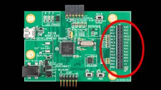
Low Cost Low Power
Instrumentation Amplifier
AD620
Rev. H
Information furnished by Analog Devices is believed to be accurate and reliable.
However, no responsibility is assumed by Analog Devices for its use, nor for any
infringements of patents or other rights of third parties that may result from its use.
Specifications subject to change without notice. No license is granted by implication
or otherwise under any patent or patent rights of Analog Devices. Trademarks and
registered trademarks are the property of their respective owners.
One Technology Way, P.O. Box 9106, Norwood, MA 02062-9106, U.S.A.
Tel: 781.329.4700 www.analog.com
Fax: 781.326.8703© 2003–2011 Analog Devices, Inc. All rights reserved.
FEATURES
Easy to use
Gain set with one external resistor
(Gain range 1 to 10,000)
Wide power supply range (±2.3 V to ±18 V)
Higher performance than 3 op amp IA designs
Available in 8-lead DIP and SOIC packaging
Low power, 1.3 mA max supply current
Excellent dc performance (B grade)
50 μV max, input offset voltage
0.6 μV/°C max, input offset drift
1.0 nA max, input bias current
100 dB min common-mode rejection ratio (G = 10)
Low noise
9 nV/√Hz @ 1 kHz, input voltage noise
0.28 μV p-p noise (0.1 Hz to 10 Hz)
Excellent ac specifications
120 kHz bandwidth (G = 100)
15 μs settling time to 0.01%
APPLICATIONS
Weigh scales
ECG and medical instrumentation
Transducer interface
Data acquisition systems
Industrial process controls
Battery-powered and portable equipment
CONNECTION DIAGRAM
–IN
RG
–VS
+IN
RG
+VS
OUTPUT
REF
1
2
3
4
8
7
6
AD620 5
TOP VIEW
00775-0-001
Figure 1. 8-Lead PDIP (N), CERDIP (Q), and SOIC (R) Packages
PRODUCT DESCRIPTION
The AD620 is a low cost, high accuracy instrumentation
amplifier that requires only one external resistor to set gains of
1 to 10,000. Furthermore, the AD620 features 8-lead SOIC and
DIP packaging that is smaller than discrete designs and offers
lower power (only 1.3 mA max supply current), making it a
good fit for battery-powered, portable (or remote) applications.
The AD620, with its high accuracy of 40 ppm maximum
nonlinearity, low offset voltage of 50 μV max, and offset drift of
0.6 μV/°C max, is ideal for use in precision data acquisition
systems, such as weigh scales and transducer interfaces.
Furthermore, the low noise, low input bias current, and low power
of the AD620 make it well suited for medical applications, such
as ECG and noninvasive blood pressure monitors.
The low input bias current of 1.0 nA max is made possible with
the use of Superϐeta processing in the input stage. The AD620
works well as a preamplifier due to its low input voltage noise of
9 nV/√Hz at 1 kHz, 0.28 μV p-p in the 0.1 Hz to 10 Hz band,
and 0.1 pA/√Hz input current noise. Also, the AD620 is well
suited for multiplexed applications with its settling time of 15 μs
to 0.01%, and its cost is low enough to enable designs with one
in-amp per channel.
Table 1. Next Generation Upgrades for AD620
Part Comment
AD8221 Better specs at lower price
AD8222 Dual channel or differential out
AD8226 Low power, wide input range
AD8220 JFET input
AD8228 Best gain accuracy
AD8295 +2 precision op amps or differential out
AD8429 Ultra low noise
0 5 10 15 20
30,000
5,000
10,000
15,000
20,000
25,000
0
TOTAL ERROR, PPM OF FULL SCALE
SUPPLY CURRENT (mA)
AD620A
RG
3 OP AMP
IN-AMP
(3 OP-07s)
00775-0-002
Figure 2. Three Op Amp IA Designs vs. AD620
IMPORTANT LINKS for the AD620*
Last content update 01/08/2014 09:49 am
Looking for a high performance in-amp with lower noise, wider bandwidth, and fast settling time? Consider the AD8421
Looking for a high performance in-amp with lower power and a rail-to-rail output? Consider the AD8422.
DOCUMENTATION
AD620: Military Data Sheet
AN-282: Fundamentals of Sampled Data Systems
AN-244: A User's Guide to I.C. Instrumentation Amplifiers
AN-245: Instrumentation Amplifiers Solve Unusual Design Problems
AN-671: Reducing RFI Rectification Errors in In-Amp Circuits
AN-589: Ways to Optimize the Performance of a Difference Amplifier
A Designer's Guide to Instrumentation Amplifiers (3rd Edition)
UG-261: Evaluation Boards for the AD62x, AD822x and AD842x Series
ECG Front-End Design is Simplified with MicroConverter
Low-Power, Low-Voltage IC Choices for ECG System Requirements
Ask The Applications Engineer-10
Auto-Zero Amplifiers
High-performance Adder Uses Instrumentation Amplifiers
Protecting Instrumentation Amplifiers
Input Filter Prevents Instrumentation-amp RF-Rectification Errors
The AD8221 - Setting a New Industry Standard for Instrumentation
Amplifiers
ADI Warns Against Misuse of COTS Integrated Circuits
Space Qualified Parts List
Applying Instrumentation Amplifiers Effectively: The Importance of an
Input Ground Return
Leading Inside Advertorials: Applying Instrumentation Amplifiers
Effectively–The Importance of an Input Ground Return
DESIGN TOOLS, MODELS, DRIVERS & SOFTWARE
In-Amp Error Calculator
These tools will help estimate error contributions in your
instrumentation amplifier circuit. It uses input parameters such as
temperature, gain, voltage input, and source impedance to determine
the errors that can contribute to your overall design.
In-Amp Common Mode Calculator
AD620 SPICE Macro-Model
AD620A SPICE Macro-Model
AD620B SPICE Macro-Model
AD620S SPICE Macro-Model
AD620 SABER Macro-Model Conv, 10/00
EVALUATION KITS & SYMBOLS & FOOTPRINTS
View the Evaluation Boards and Kits page for documentation and
purchasing
Symbols and Footprints
PRODUCT RECOMMENDATIONS & REFERENCE DESIGNS
CN-0146: Low Cost Programmable Gain Instrumentation Amplifier
Circuit Using the ADG1611 Quad SPST Switch and AD620
Instrumentation Amplifier
DESIGN COLLABORATION COMMUNITY
Collaborate Online with the ADI support team and other designers
about select ADI products.
Follow us on Twitter: www.twitter.com/ADI_News
Like us on Facebook: www.facebook.com/AnalogDevicesInc
DESIGN SUPPORT
Submit your support request here:
Linear and Data Converters
Embedded Processing and DSP
Telephone our Customer Interaction Centers toll free:
Americas: 1-800-262-5643
Europe: 00800-266-822-82
China: 4006-100-006
India: 1800-419-0108
Russia: 8-800-555-45-90
Quality and Reliability
Lead(Pb)-Free Data
SAMPLE & BUY
AD620
View Price & Packaging
Request Evaluation Board
Request Samples Check Inventory & Purchase
Find Local Distributors
* This page was dynamically generated by Analo g Devices, Inc. and inserted into this data sheet.
Note: Dynamic changes to the content on this page (labeled 'Important Links') does not
constitute a change to the revision number of the product data sheet.
This content may be frequently modified.
Powered by TCPDF (www.tcpdf.org)
AD620
Rev. H | Page 2 of 20
TABLE OF CONTENTS
Specifications .....................................................................................3
Absolute Maximum Ratings ............................................................5
ESD Caution ..................................................................................5
Typical Performance Characteristics..............................................6
Theory of Operation.......................................................................12
Gain Selection..............................................................................15
Input and Output Offset Voltage ..............................................15
Reference Terminal .....................................................................15
Input Protection ..........................................................................15
RF Interference............................................................................15
Common-Mode Rejection.........................................................16
Grounding....................................................................................16
Ground Returns for Input Bias Currents.................................17
AD620ACHIPS Information.........................................................18
Outline Dimensions........................................................................19
Ordering Guide ...........................................................................20
REVISION HISTORY
7/11—Rev. G to Rev. H
Deleted Figure 3.................................................................................1
Added Table 1 ....................................................................................1
Moved Figure 2 ..................................................................................1
Added ESD Input Diodes to Simplified Schematic ....................12
Changes to Input Protection Section............................................15
Added Figure 41; Renumbered Sequentially ...............................15
Changes to AD620ACHIPS Information Section ......................18
Updated Ordering Guide ...............................................................20
12/04—Rev. F to Rev. G
Updated Format..................................................................Universal
Change to Features............................................................................1
Change to Product Description.......................................................1
Changes to Specifications.................................................................3
Added Metallization Photograph....................................................4
Replaced Figure 4-Figure 6 ..............................................................6
Replaced Figure 15............................................................................7
Replaced Figure 33..........................................................................10
Replaced Figure 34 and Figure 35.................................................10
Replaced Figure 37..........................................................................10
Changes to Table 3 ..........................................................................13
Changes to Figure 41 and Figure 42 .............................................14
Changes to Figure 43 ......................................................................15
Change to Figure 44 ........................................................................17
Changes to Input Protection section ............................................15
Deleted Figure 9 ..............................................................................15
Changes to RF Interference section..............................................15
Edit to Ground Returns for Input Bias Currents section...........17
Added AD620CHIPS to Ordering Guide ....................................19
7/03—Data Sheet Changed from Rev. E to Rev. F
Edit to FEATURES............................................................................1
Changes to SPECIFICATIONS.......................................................2
Removed AD620CHIPS from ORDERING GUIDE ...................4
Removed METALLIZATION PHOTOGRAPH...........................4
Replaced TPCs 1–3 ...........................................................................5
Replaced TPC 12...............................................................................6
Replaced TPC 30...............................................................................9
Replaced TPCs 31 and 32...............................................................10
Replaced Figure 4............................................................................10
Changes to Table I...........................................................................11
Changes to Figures 6 and 7 ............................................................12
Changes to Figure 8 ........................................................................13
Edited INPUT PROTECTION section........................................13
Added new Figure 9........................................................................13
Changes to RF INTERFACE section ............................................14
Edit to GROUND RETURNS FOR INPUT BIAS CURRENTS
section...............................................................................................15
Updated OUTLINE DIMENSIONS.............................................16
AD620
Rev. H | Page 3 of 20
SPECIFICATIONS
Typical @ 25°C, VS = ±15 V, and RL = 2 kΩ, unless otherwise noted.
Table 2.
Parameter Conditions
AD620A AD620B AD620S1
Min Typ Max Min Typ Max Min Typ Max Unit
GAIN G = 1 + (49.4 kΩ/RG)
Gain Range 1 10,000 1 10,000 1 10,000
Gain Error2 VOUT = ±10 V
G = 1 0.03 0.10 0.01 0.02 0.03 0.10 %
G = 10 0.15 0.30 0.10 0.15 0.15 0.30 %
G = 100 0.15 0.30 0.10 0.15 0.15 0.30 %
G = 1000 0.40 0.70 0.35 0.50 0.40 0.70 %
Nonlinearity VOUT = −10 V to +10 V
G = 1–1000 RL = 10 kΩ 10 40 10 40 10 40 ppm
G = 1–100 RL = 2 kΩ 10 95 10 95 10 95 ppm
Gain vs. Temperature
G = 1 10 10 10 ppm/°C
Gain >12 −50 −50 −50 ppm/°C
VOLTAGE OFFSET (Total RTI Error = VOSI + VOSO/G)
Input Offset, VOSI VS = ±5 V
to ± 15 V
30 125 15 50 30 125 μV
Overtemperature VS = ±5 V
to ± 15 V
185 85 225 μV
Average TC VS = ±5 V
to ± 15 V
0.3 1.0 0.1 0.6 0.3 1.0 μV/°C
Output Offset, VOSO VS = ±15 V 400 1000 200 500 400 1000 μV
VS = ± 5 V 1500 750 1500 μV
Overtemperature VS = ±5 V
to ± 15 V
2000 1000 2000 μV
Average TC VS = ±5 V
to ± 15 V
5.0 15 2.5 7.0 5.0 15 μV/°C
Offset Referred to the
Input vs. Supply (PSR) VS = ±2.3 V
to ±18 V
G = 1 80 100 80 100 80 100 dB
G = 10 95 120 100 120 95 120 dB
G = 100 110 140 120 140 110 140 dB
G = 1000 110 140 120 140 110 140 dB
INPUT CURRENT
Input Bias Current 0.5 2.0 0.5 1.0 0.5 2 nA
Overtemperature 2.5 1.5 4 nA
Average TC 3.0 3.0 8.0 pA/°C
Input Offset Current 0.3 1.0 0.3 0.5 0.3 1.0 nA
Overtemperature 1.5 0.75 2.0 nA
Average TC 1.5 1.5 8.0 pA/°C
INPUT
Input Impedance
Differential 10||2 10||2 10||2 GΩ_pF
Common-Mode 10||2 10||2 10||2 GΩ_pF
Input Voltage Range3 VS = ±2.3 V
to ±5 V
−VS + 1.9 +VS − 1.2 −VS + 1.9 +VS − 1.2 −VS + 1.9 +VS − 1.2 V
Overtemperature −VS + 2.1 +VS − 1.3 −VS + 2.1 +VS − 1.3 −VS + 2.1 +VS − 1.3 V
VS = ± 5 V
to ±18 V
−VS + 1.9 +VS − 1.4 −VS + 1.9 +VS − 1.4 −VS + 1.9 +VS − 1.4 V
Overtemperature −VS + 2.1 +VS − 1.4 −VS + 2.1 +VS + 2.1 −VS + 2.3 +VS − 1.4 V
AD620
Rev. H | Page 4 of 20
AD620A AD620B AD620S1
Parameter Conditions Min Typ Max Min Typ Max Min Typ Max Unit
Common-Mode Rejection
Ratio DC to 60 Hz with
1 kΩ Source Imbalance VCM = 0 V to ± 10 V
G = 1 73 90 80 90 73 90 dB
G = 10 93 110 100 110 93 110 dB
G = 100 110 130 120 130 110 130 dB
G = 1000 110 130 120 130 110 130 dB
OUTPUT
Output Swing RL = 10 kΩ
VS = ±2.3 V
to ± 5 V
−VS +
1.1
+VS − 1.2 −VS + 1.1 +VS − 1.2 −VS + 1.1 +VS − 1.2 V
Overtemperature −VS + 1.4 +VS − 1.3 −VS + 1.4 +VS − 1.3 −VS + 1.6 +VS − 1.3 V
VS = ±5 V
to ± 18 V
−VS + 1.2 +VS − 1.4 −VS + 1.2 +VS − 1.4 −VS + 1.2 +VS − 1.4 V
Overtemperature −VS + 1.6 +VS – 1.5 −VS + 1.6 +VS – 1.5 –VS + 2.3 +VS – 1.5 V
Short Circuit Current ±18 ±18 ±18 mA
DYNAMIC RESPONSE
Small Signal –3 dB Bandwidth
G = 1 1000 1000 1000 kHz
G = 10 800 800 800 kHz
G = 100 120 120 120 kHz
G = 1000 12 12 12 kHz
Slew Rate 0.75 1.2 0.75 1.2 0.75 1.2 V/μs
Settling Time to 0.01% 10 V Step
G = 1–100 15 15 15 μs
G = 1000 150 150 150 μs
NOISE
Voltage Noise, 1 kHz Total RTI Noise (e2 ) (e /G)2 = ni + no
Input, Voltage Noise, eni 9 13 9 13 9 13 nV/√Hz
Output, Voltage Noise, eno 72 100 72 100 72 100 nV/√Hz
RTI, 0.1 Hz to 10 Hz
G = 1 3.0 3.0 6.0 3.0 6.0 μV p-p
G = 10 0.55 0.55 0.8 0.55 0.8 μV p-p
G = 100–1000 0.28 0.28 0.4 0.28 0.4 μV p-p
Current Noise f = 1 kHz 100 100 100 fA/√Hz
0.1 Hz to 10 Hz 10 10 10 pA p-p
REFERENCE INPUT
RIN 20 20 20 kΩ
IIN VIN+, VREF = 0 50 60 50 60 50 60 μA
Voltage Range −VS + 1.6 +VS − 1.6 −VS + 1.6 +VS − 1.6 −VS + 1.6 +VS − 1.6 V
Gain to Output 1 ± 0.0001 1 ± 0.0001 1 ± 0.0001
POWER SUPPLY
Operating Range4 ±2.3 ±18 ±2.3 ±18 ±2.3 ±18 V
Quiescent Current VS = ±2.3 V
to ±18 V
0.9 1.3 0.9 1.3 0.9 1.3 mA
Overtemperature 1.1 1.6 1.1 1.6 1.1 1.6 mA
TEMPERATURE RANGE
For Specified Performance −40 to +85 −40 to +85 −55 to +125 °C
1 See Analog Devices military data sheet for 883B tested specifications.
2 Does not include effects of external resistor RG.
3 One input grounded. G = 1.
4 This is defined as the same supply range that is used to specify PSR.
AD620
Rev. H | Page 5 of 20
ABSOLUTE MAXIMUM RATINGS
Table 3.
Parameter Rating
Supply Voltage ±18 V
Internal Power Dissipation1 650 mW
Input Voltage (Common-Mode) ±VS
Differential Input Voltage 25 V
Output Short-Circuit Duration Indefinite
Storage Temperature Range (Q) −65°C to +150°C
Storage Temperature Range (N, R) −65°C to +125°C
Operating Temperature Range
AD620 (A, B) −40°C to +85°C
AD620 (S) −55°C to +125°C
Lead Temperature Range
(Soldering 10 seconds) 300°C
1 Specification is for device in free air:
8-Lead Plastic Package: θJA = 95°C
8-Lead CERDIP Package: θJA = 110°C
8-Lead SOIC Package: θJA = 155°C
Stresses above those listed under Absolute Maximum Ratings
may cause permanent damage to the device. This is a stress
rating only; functional operation of the device at these or any
other condition s above those indicated in the operational
section of this specification is not implied. Exposure to absolute
maximum rating conditions for extended periods may affect
device reliability.
ESD CAUTION
AD620
Rev. H | Page 6 of 20
TYPICAL PERFORMANCE CHARACTERISTICS
(@ 25°C, VS = ±15 V, RL = 2 kΩ, unless otherwise noted.)
INPUT OFFSET VOLTAGE (μV)
20
30
40
50
–40 0 40 80
PERCENTAGE OF UNITS
–80
SAMPLE SIZE = 360
10
0
00775-0-005
Figure 3. Typical Distribution of Input Offset Voltage
INPUT BIAS CURRENT (pA)
0
10
20
30
40
50
–600 0 600
PERCENTAGE OF UNITS
–1200 1200
SAMPLE SIZE = 850
00775-0-006
Figure 4. Typical Distribution of Input Bias Current
10
20
30
40
50
–200 0 200 400
INPUT OFFSET CURRENT (pA)
PERCENTAGE OF UNITS
–400
0
SAMPLE SIZE = 850 00775-0-007
Figure 5. Typical Distribution of Input Offset Current
TEMPERATURE (°C)
INPUT BIAS CURRENT (nA)
+IB
–IB
2.0
–2.0
175
–1.0
–1.5
–75
–0.5
0
0.5
1.0
1.5
–25 25 75 125
00775-0-008
Figure 6. Input Bias Current vs. Temperature
CHANGE IN OFFSET VOLTAGE (μV)
1.5
0.5
WARM-UP TIME (Minutes)
2.0
0
0 1
1.0
2 3 4 5
00775-0-009
Figure 7. Change in Input Offset Voltage vs. Warm-Up Time
FREQUENCY (Hz)
1000
1
1 100k
100
10
100 1k 10k
VOLTAGE NOISE (nV/ Hz)
GAIN = 1
GAIN = 10
10
GAIN = 100, 1,000
GAIN = 1000
BW LIMIT
00775-0-010
Figure 8. Voltage Noise Spectral Density vs. Frequency (G = 1−1000)
AD620
Rev. H | Page 7 of 20
FREQUENCY (Hz)
1000
100
10
1 10 100 1000
CURRENT NOISE (fA/ Hz)
00775-0-011
Figure 9. Current Noise Spectral Density vs. Frequency
RTI NOISE (2.0μV/DIV)
TIME (1 SEC/DIV)
00775-0-012
Figure 10. 0.1 Hz to 10 Hz RTI Voltage Noise (G = 1)
RTI NOISE (0.1μV/DIV)
TIME (1 SEC/DIV)
00775-0-013
Figure 11. 0.1 Hz to 10 Hz RTI Voltage Noise (G = 1000)
00775-0-014
Figure 12. 0.1 Hz to 10 Hz Current Noise, 5 pA/Div
100
1000
AD620A
FET INPUT
IN-AMP
SOURCE RESISTANCE (Ω)
TOTAL DRIFT FROM 25°C TO 85°C, RTI (μV)
100,000
10
1k 10M
10,000
10k 100k 1M
00775-0-015
Figure 13. Total Drift vs. Source Resistance
FREQUENCY (Hz)
CMR (dB)
160
0
1M
80
40
1
60
0.1
140
100
120
10 100 1k 10k 100k
G = 1000
G = 100
G = 10
G = 1
20
00775-0-016
Figure 14. Typical CMR vs. Frequency, RTI, Zero to 1 kΩ Source Imbalance
AD620
Rev. H | Page 8 of 20
FREQUENCY (Hz)
PSR (dB)
160
1M
80
40
1
60
0.1
140
100
120
10 100 1k 10k 100k
20
G = 1000
G = 100
G = 10
G = 1
180
00775-0-017
Figure 15. Positive PSR vs. Frequency, RTI (G = 1−1000)
FREQUENCY (Hz)
PSR (dB)
160
1M
80
40
1
60
0.1
140
100
120
10 100 1k 10k 100k
20
180
G = 10
G = 100
G = 1
G = 1000
00775-0-018
Figure 16. Negative PSR vs. Frequency, RTI (G = 1−1000)
1000
100 10M
100
1
1k
10
10k 100k 1M
FREQUENCY (Hz)
GAIN (V/V)
0.1
00775-0-019
Figure 17. Gain vs. Frequency
OUTPUT VOLTAGE (V p-p)
FREQUENCY (Hz)
35
0
1M
15
5
10k
10
1k
30
20
25
100k
G = 10, 100, 1000
G = 1
G = 1000 G = 100
BW LIMIT
00775-0-020
Figure 18. Large Signal Frequency Response
INPUT VOLTAGE LIMIT (V)
(REFERRED TO SUPPLY VOLTAGES) 20
+1.0
+0.5
0 5
+1.5
–1.5
–1.0
–0.5
10 15
SUPPLY VOLTAGE ± Volts
+VS –0.0
–VS +0.0
00775-0-021
Figure 19. Input Voltage Range vs. Supply Voltage, G = 1
20
+1.0
+0.5
0 5
+1.5
–1.5
–1.0
–0.5
10 15
SUPPLY VOLTAGE ± Volts
RL = 10kΩ
RL = 2kΩ
RL = 10kΩ
OUTPUT VOLTAGE SWING (V)
(REFERRED TO SUPPLY VOLTAGES)
RL = 2kΩ
+VS
–VS
00775-0-022
–0.0
+0.0
Figure 20. Output Voltage Swing vs. Supply Voltage, G = 10
AD620
Rev. H | Page 9 of 20
OUTPUT VOLTAGE SWING (V p-p)
LOAD RESISTANCE (Ω)
30
0
0 10k
20
10
100 1k
VS = ±15V
G = 10
00775-0-023
Figure 21. Output Voltage Swing vs. Load Resistance
. . . . . . . . . . . . . . . . . . . . . . . . . . . . . . . . . . . . . . . .
. . . . . . . . . . . . . . . . . . . . . . . . . . . . . . . . . . . . . . . .
00775-0-024
Figure 22. Large Signal Pulse Response and Settling Time
G = 1 (0.5 mV = 0.01%)
. . . . . . . . . . . . . . . . . . . . . . . . . . . . . . . . . . . . . . . .
. . . . . . . . . . . . . . . . . . . . . . . . . . . . . . . . . . . . . . . . 00775-0-025
Figure 23. Small Signal Response, G = 1, RL = 2 kΩ, CL = 100 pF
. . . . . . . . . . . . . . . . . . . . . . . . . . . . . . . . . . . . . . . .
. . . . . . . . . . . . . . . . . . . . . . . . . . . . . . . . . . . . . . . .
00775-0-026
Figure 24. Large Signal Response and Settling Time, G = 10 (0.5 mV = 0.01%)
. . . . . . . . . . . . . . . . . . . . . . . . . . . . . . . . . . . . . . . .
. . . . . . . . . . . . . . . . . . . . . . . . . . . . . . . . . . . . . . . .
00775-0-027
Figure 25. Small Signal Response, G = 10, RL = 2 kΩ, CL = 100 pF
. . . . . . . . . . . . . . . . . . . . . . . . . . . . . . . . . . . . . . . .
. . . . . . . . . . . . . . . . . . . . . . . . . . . . . . . . . . . . . . . .
00775-0-030
Figure 26. Large Signal Response and Settling Time, G = 100 (0.5 mV = 0.01%)
AD620
Rev. H | Page 10 of 20
. . . . . . . . . . . . . . . . . . . . . . . . . . . . . . . . . . . . . . . .
. . . . . . . . . . . . . . . . . . . . . . . . . . . . . . . . . . . . . . . .
00775-0-029
Figure 27. Small Signal Pulse Response, G = 100, RL = 2 kΩ, CL = 100 pF
. . . . . . . . . . . . . . . . . . . . . . . . . . . . . . . . . . . . . . . .
. . . . . . . . . . . . . . . . . . . . . . . . . . . . . . . . . . . . . . . .
00775-0-030
Figure 28. Large Signal Response and Settling Time,
G = 1000 (0.5 mV = 0.01% )
. . . . . . . . . . . . . . . . . . . . . . . . . . . . . . . . . . . . . . . .
. . . . . . . . . . . . . . . . . . . . . . . . . . . . . . . . . . . . . . . .
00775-0-031
Figure 29. Small Signal Pulse Response, G = 1000, RL = 2 kΩ, CL = 100 pF
OUTPUT STEP SIZE (V)
SETTLING TIME (μs)
TO 0.01%
TO 0.1%
20
0
0 2
15
5
5
10
10 15 0
00775-0-032
Figure 30. Settling Time vs. Step Size (G = 1)
GAIN
SETTLING TIME (μs)
1000
1
1 1000
100
10
10 100
00775-0-033
Figure 31. Settling Time to 0.01% vs. Gain, for a 10 V Step
. . . . . . . . . . . . . . . . . . . . . . . . . . . . . . . . . . . . . . . .
. . . . . . . . . . . . . . . . . . . . . . . . . . . . . . . . . . . . . . . .
00775-0-034
Figure 32. Gain Nonlinearity, G = 1, RL = 10 kΩ (10 μV = 1 ppm)
AD620
Rev. H | Page 11 of 20
. . . . . . . . . . . . . . . . . . . . . . . . . . . . . . . . . . . . . . . .
. . . . . . . . . . . . . . . . . . . . . . . . . . . . . . . . . . . . . . . .
00775-0-035
Figure 33. Gain Nonlinearity, G = 100, RL = 10 kΩ
(100 μV = 10 ppm)
. . . . . . . . . . . . . . . . . . . . . . . . . . . . . . . . . . . . . . . .
. . . . . . . . . . . . . . . . . . . . . . . . . . . . . . . . . . . . . . . .
00775-0-036
Figure 34. Gain Nonlinearity, G = 1000, RL = 10 kΩ
(1 mV = 100 ppm)
AD620
VOUT
G = 1000 G = 1
49.9Ω
10kΩ *
1kΩ
10T 10kΩ
499Ω
G = 100 G = 10
5.49kΩ
+VS
11kΩ 1kΩ 100Ω
100kΩ
INPUT
10V p-p
–VS
*ALL RESISTORS 1% TOLERANCE
1 7
2
3
8
6
4
5
00775-0-037
Figure 35. Settling Time Test Circuit
AD620
Rev. H | Page 12 of 20
THEORY OF OPERATION
VB
–VS
A1 A2
A3
C2
RG
R1 R2
GAIN
SENSE
GAIN
SENSE
10kΩ
10kΩ
I1 I2
10kΩ
REF
10kΩ
+IN
– IN R4
400Ω
OUTPUT
C1
Q1 Q2
00775-0-038
R3
400Ω
+VS +VS
+VS
20μA 20μA
Figure 36. Simplified Schematic of AD620
The AD620 is a monolithic instrumentation amplifier based on
a modification of the classic three op amp approach. Absolute
value trimming allows the user to program gain accurately
(to 0.15% at G = 100) with only one resistor. Monolithic
construction and laser wafer trimming allow the tight matching
and tracking of circuit components, thus ensuring the high level
of performance inherent in this circuit.
The input transistors Q1 and Q2 provide a single differentialpair
bipolar input for high precision (Figure 36), yet offer 10×
lower input bias current thanks to Superϐeta processing.
Feedback through the Q1-A1-R1 loop and the Q2-A2-R2 loop
maintains constant collector current of the input devices Q1
and Q2, thereby impressing the input voltage across the external
gain setting resistor RG. This creates a differential gain from the
inputs to the A1/A2 outputs given by G = (R1 + R2)/RG + 1. The
unity-gain subtractor, A3, removes any common-mode signal,
yielding a single-ended output referred to the REF pin potential.
The value of RG also determines the transconductance of the
preamp stage. As RG is reduced for larger gains, the
transconductance increases asymptotically to that of the input
transistors. This has three important advantages: (a) Open-loop
gain is boosted for increasing programmed gain, thus reducing
gain related errors. (b) The gain-bandwidth product
(determined by C1 and C2 and the preamp transconductance)
increases with programmed gain, thus optimizing frequency
response. (c) The input voltage noise is reduced to a value of
9 nV/√Hz, determined mainly by the collector current and base
resistance of the input devices.
The internal gain resistors, R1 and R2, are trimmed to an
absolute value of 24.7 kΩ, allowing the gain to be programmed
accurately with a single external resistor.
The gain equation is then
1
49.4 +
Ω
=
RG
k
G
1
49.4
−
Ω
=
G
k
RG
Make vs. Buy: a Typical Bridge Application Error Budget
The AD620 offers improved performance over “homebrew”
three op amp IA designs, along with smaller size, fewer
components, and 10× lower supply current. In the typical
application, shown in Figure 37, a gain of 100 is required to
amplify a bridge output of 20 mV full-scale over the industrial
temperature range of −40°C to +85°C. Table 4 shows how to
calculate the effect various error sources have on circuit
accuracy.
AD620
Rev. H | Page 13 of 20
Regardless of the system in which it is being used, the AD620
provides greater accuracy at low power and price. In simple
systems, absolute accuracy and drift errors are by far the most
significant contributors to error. In more complex systems
with an intelligent processor, an autogain/autozero cycle
removes all absolute accuracy and drift errors, leaving only the
resolution errors of gain, nonlinearity, and noise, thus allowing
full 14-bit accuracy.
Note that for the homebrew circuit, the OP07 specifications for
input voltage offset and noise have been multiplied by √2. This
is because a three op amp type in-amp has two op amps at its
inputs, both contributing to the overall input error.
R = 350Ω
10V
PRECISION BRIDGE TRANSDUCER
R = 350Ω R = 350Ω
R = 350Ω
00775-0-039
AD620A MONOLITHIC
INSTRUMENTATION
AMPLIFIER, G = 100
SUPPLY CURRENT = 1.3mA MAX
AD620A RG
499Ω
REFERENCE
00775-0-040
Figure 37. Make vs. Buy
"HOMEBREW" IN-AMP, G = 100
*0.02% RESISTOR MATCH, 3ppm/°C TRACKING
**DISCRETE 1% RESISTOR, 100ppm/°C TRACKING
SUPPLY CURRENT = 15mA MAX
100Ω **
10kΩ *
10kΩ **
10kΩ *
10kΩ *
10kΩ **
10kΩ*
OP07D
OP07D
OP07D
00775-0-041
Table 4. Make vs. Buy Error Budget
Error, ppm of Full Scale
Error Source AD620 Circuit Calculation “Homebrew” Circuit Calculation AD620 Homebrew
ABSOLUTE ACCURACY at TA = 25°C
Input Offset Voltage, μV 125 μV/20 mV (150 μV × √2)/20 mV 6,250 10,607
Output Offset Voltage, μV 1000 μV/100 mV/20 mV ((150 μV × 2)/100)/20 mV 500 150
Input Offset Current, nA 2 nA ×350 Ω/20 mV (6 nA ×350 Ω)/20 mV 18 53
CMR, dB 110 dB(3.16 ppm) ×5 V/20 mV (0.02% Match × 5 V)/20 mV/100 791 500
Total Absolute Error 7,559 11,310
DRIFT TO 85°C
Gain Drift, ppm/°C (50 ppm + 10 ppm) ×60°C 100 ppm/°C Track × 60°C 3,600 6,000
Input Offset Voltage Drift, μV/°C 1 μV/°C × 60°C/20 mV (2.5 μV/°C × √2 × 60°C)/20 mV 3,000 10,607
Output Offset Voltage Drift, μV/°C 15 μV/°C × 60°C/100 mV/20 mV (2.5 μV/°C × 2 × 60°C)/100 mV/20 mV 450 150
Total Drift Error 7,050 16,757
RESOLUTION
Gain Nonlinearity, ppm of Full Scale 40 ppm 40 ppm 40 40
Typ 0.1 Hz to 10 Hz Voltage Noise, μV p-p 0.28 μV p-p/20 mV (0.38 μV p-p × √2)/20 mV 14 27
Total Resolution Error 54 67
Grand Total Error 14,663 28,134
G = 100, VS = ±15 V.
(All errors are min/max and referred to input.)
AD620
Rev. H | Page 14 of 20
3kΩ
5V
DIGITAL
DATA
OUTPUT
ADC
REF
IN
AGND
20kΩ
10kΩ
20kΩ
G = 100 AD620B
1.7mA 0.10mA 0.6mA
MAX
499Ω
3kΩ
3kΩ 3kΩ
2
1
8
3 7
6
5
4
1.3mA
MAX
AD705
00775-0-042
Figure 38. A Pressure Monitor Circuit that Operates on a 5 V Single Supply
Pressure Measurement
Although useful in many bridge applications, such as weigh
scales, the AD620 is especially suitable for higher resistance
pressure sensors powered at lower voltages where small size and
low power become more significant.
Figure 38 shows a 3 kΩ pressure transducer bridge powered
from 5 V. In such a circuit, the bridge consumes only 1.7 mA.
Adding the AD620 and a buffered voltage divider allows the
signal to be conditioned for only 3.8 mA of total supply current.
Small size and low cost make the AD620 especially attractive for
voltage output pressure transducers. Since it delivers low noise
and drift, it also serves applications such as diagnostic
noninvasive blood pressure measurement.
Medical ECG
The low current noise of the AD620 allows its use in ECG
monitors (Figure 39) where high source resistances of 1 MΩ or
higher are not uncommon. The AD620’s low power, low supply
voltage requirements, and space-saving 8-lead mini-DIP and
SOIC package offerings make it an excellent choice for batterypowered
data recorders.
Furthermore, the low bias currents and low current noise,
coupled with the low voltage noise of the AD620, improve the
dynamic range for better performance.
The value of capacitor C1 is chosen to maintain stability of
the right leg drive loop. Proper safeguards, such as isolation,
must be added to this circuit to protect the patient from
possible harm.
G = 7
AD620A
0.03Hz
HIGHPASS
FILTER
OUTPUT
1V/mV
+3V
–3V
RG
8.25kΩ
24.9kΩ
24.9kΩ
AD705J
G = 143
C1
1MΩ
R4
10kΩ
R1 R3
R2
OUTPUT
AMPLIFIER
PATIENT/CIRCUIT
PROTECTION/ISOLATION
00775-0-043
Figure 39. A Medical ECG Monitor Circuit
AD620
Rev. H | Page 15 of 20
Precision V-I Converter
The AD620, along with another op amp and two resistors,
makes a precision current source (Figure 40). The op amp
buffers the reference terminal to maintain good CMR. The
output voltage, VX, of the AD620 appears across R1, which
converts it to a current. This current, less only the input bias
current of the op amp, then flows out to the load.
RG AD620
–VS
VIN+
VIN–
LOAD
R1
IL
Vx I L = R1
= IN+ [(V ) – (V IN – )] G
R1
6
5
+ VX –
2 4
1
8
3 7
+VS
AD705
00775-0-044
Figure 40. Precision Voltage-to-Current Converter (Operates on 1.8 mA, ±3 V)
GAIN SELECTION
The AD620 gain is resistor-programmed by RG, or more
precisely, by whatever impedance appears between Pins 1 and 8.
The AD620 is designed to offer accurate gains using 0.1% to 1%
resistors. Table 5 shows required values of RG for various gains.
Note that for G = 1, the RG pins are unconnected (RG = ∞). For
any arbitrary gain, RG can be calculated by using the formula:
1
49.4
−
Ω
=
G
k
RG
To minimize gain error, avoid high parasitic resistance in series
with RG; to minimize gain drift, RG should have a low TC—less
than 10 ppm/°C—for the best performance.
Table 5. Required Values of Gain Resistors
1% Std Table
Value of RG(Ω)
Calculated
Gain
0.1% Std Table
Value of RG(Ω )
Calculated
Gain
49.9 k 1.990 49.3 k 2.002
12.4 k 4.984 12.4 k 4.984
5.49 k 9.998 5.49 k 9.998
2.61 k 19.93 2.61 k 19.93
1.00 k 50.40 1.01 k 49.91
499 100.0 499 100.0
249 199.4 249 199.4
100 495.0 98.8 501.0
49.9 991.0 49.3 1,003.0
INPUT AND OUTPUT OFFSET VOLTAGE
The low errors of the AD620 are attributed to two sources,
input and output errors. The output error is divided by G when
referred to the input. In practice, the input errors dominate at
high gains, and the output errors dominate at low gains. The
total VOS for a given gain is calculated as
Total Error RTI = input error + (output error/G)
Total Error RTO = (input error × G) + output error
REFERENCE TERMINAL
The reference terminal potential defines the zero output voltage
and is especially useful when the load does not share a precise
ground with the rest of the system. It provides a direct means of
injecting a precise offset to the output, with an allowable range
of 2 V within the supply voltages. Parasitic resistance should be
kept to a minimum for optimum CMR.
INPUT PROTECTION
The AD620 safely withstands an input current of ±60 mA for
several hours at room temperature. This is true for all gains and
power on and off, which is useful if the signal source and
amplifier are powered separately. For longer time periods, the
input current should not exceed 6 mA.
For input voltages beyond the supplies, a protection resistor
should be placed in series with each input to limit the current to
6 mA. These can be the same resistors as those used in the RFI
filter. High values of resistance can impact the noise and AC
CMRR performance of the system. Low leakage diodes (such as
the BAV199) can be placed at the inputs to reduce the required
protection resistance.
AD620
R
REF
R
+SUPPLY
–SUPPLY
VOUT
+IN
–IN
00775-0-052
Figure 41. Diode Protection for Voltages Beyond Supply
RF INTERFERENCE
All instrumentation amplifiers rectify small out of band signals.
The disturbance may appear as a small dc voltage offset. High
frequency signals can be filtered with a low pass R-C network
placed at the input of the instrumentation amplifier. Figure 42
demonstrates such a configuration. The filter limits the input
AD620
Rev. H | Page 16 of 20
signal according to the following relationship:
2 (2 )
1
D C
DIFF R C C
FilterFreq
π +
=
C
CM RC
FilterFreq
π
=
2
1
where CD ≥10CC.
CD affects the difference signal. CC affects the common-mode
signal. Any mismatch in R × CC degrades the AD620 CMRR. To
avoid inadvertently reducing CMRR-bandwidth performance,
make sure that CC is at least one magnitude smaller than CD.
The effect of mismatched CCs is reduced with a larger CD:CC
ratio.
499Ω AD620
+
–
VOUT
R
R
CC
CD
CC +IN
–IN REF
–15V
0.1μ F 10μ F
+15V
0.1μ F 10μ F
00775-0-045
Figure 42. Circuit to Attenuate RF Interference
COMMON-MODE REJECTION
Instrumentation amplifiers, such as the AD620, offer high
CMR, which is a measure of the change in output voltage when
both inputs are changed by equal amounts. These specifications
are usually given for a full-range input voltage change and a
specified source imbalance.
For optimal CMR, the reference terminal should be tied to a
low impedance point, and differences in capacitance and
resistance should be kept to a minimum between the two
inputs. In many applications, shielded cables are used to
minimize noise; for best CMR over frequency, the shield
should be properly driven. Figure 43 and Figure 44 show active
data guards that are configured to improve ac common-mode
rejections by “bootstrapping” the capacitances of input cable
shields, thus minimizing the capacitance mismatch between the
inputs.
REFERENCE
VOUT AD620
100Ω
100Ω
– INPUT
+ INPUT
AD648
RG
–VS
+VS
–VS
00775-0-046
Figure 43. Differential Shield Driver
100Ω
– INPUT
+ INPUT
REFERENCE
VOUT AD620
–VS
+VS
2
RG
2
RG AD548
00775-0-047
Figure 44. Common-Mode Shield Driver
GROUNDING
Since the AD620 output voltage is developed with respect to the
potential on the reference terminal, it can solve many
grounding problems by simply tying the REF pin to the
appropriate “local ground.”
To isolate low level analog signals from a noisy digital
environment, many data-acquisition components have separate
analog and digital ground pins (Figure 45). It would be
convenient to use a single ground line; however, current
through ground wires and PC runs of the circuit card can cause
hundreds of millivolts of error. Therefore, separate ground
returns should be provided to minimize the current flow from
the sensitive points to the system ground. These ground returns
must be tied together at some point, usually best at the ADC
package shown in Figure 45.
DIGITAL P.S.
C +5V
ANALOG P.S.
+15V C –15V
AD574A DIGITAL
DATA
OUTPUT
+
1μF
AD620
0.1μF
AD585
S/H ADC
0.1μF
1μF 1μF
00775-0-048
Figure 45. Basic Grounding Practice
AD620
Rev. H | Page 17 of 20
GROUND RETURNS FOR INPUT BIAS CURRENTS
VOUT
– INPUT
+ INPUT
RG
LOAD
TO POWER
SUPPLY
GROUND
REFERENCE
+VS
–VS
AD620
00775-0-050
Input bias currents are those currents necessary to bias the
input transistors of an amplifier. There must be a direct return
path for these currents. Therefore, when amplifying “floating”
input sources, such as transformers or ac-coupled sources, there
must be a dc path from each input to ground, as shown in
Figure 46, Figure 47, and Figure 48. Refer to A Designer’s Guide
to Instrumentation Amplifiers (free from Analog Devices) for
more information regarding in-amp applications.
AD620 VOUT
– INPUT
RG
TO POWER
SUPPLY
GROUND
+ INPUT REFERENCE
+VS
–VS
LOAD
00775-0-049
Figure 47. Ground Returns for Bias Currents with Thermocouple Inputs
100kΩ
AD620 VOUT
– INPUT
+ INPUT
RG
LOAD
TO POWER
SUPPLY
GROUND
REFERENCE
100kΩ –VS
+VS
00775-0-051
Figure 46. Ground Returns for Bias Currents with Transformer-Coupled Inputs
Figure 48. Ground Returns for Bias Currents with AC-Coupled Inputs
AD620
Rev. H | Page 18 of 20
AD620ACHIPS INFORMATION
Die size: 1803 μm × 3175 μm
Die thickness: 483 μm
Bond Pad Metal: 1% Copper Doped Aluminum
To minimize gain errors introduced by the bond wires, use Kelvin connections between the chip and the gain resistor, RG, by connecting
Pad 1A and Pad 1B in parallel to one end of RG and Pad 8A and Pad 8B in parallel to the other end of RG. For unity gain applications
where RG is not required, Pad 1A and Pad 1B must be bonded together as well as the Pad 8A and Pad 8B.
1A
1B
2
3
4 5
6
7
8A
8B
LOGO
00775-0-053
Figure 49. Bond Pad Diagram
Table 6. Bond Pad Information
Pad Coordinates1
Pad No. Mnemonic X (μm) Y (μm)
1A RG −623 +1424
1B RG −789 +628
2 −IN −790 +453
3 +IN −790 −294
4 −VS −788 −1419
5 REF +570 −1429
6 OUTPUT +693 −1254
7 +VS +693 +139
8A RG +505 +1423
8B RG +693 +372
1 The pad coordinates indicate the center of each pad, referenced to the center of the die. The die orientation is indicated by the logo, as shown in Figure 49.
AD620
Rev. H | Page 19 of 20
OUTLINE DIMENSIONS
COMPLIANT TO JEDEC STANDARDS MS-001
CONTROLLING DIMENSIONS ARE IN INCHES; MILLIMETER DIMENSIONS
(IN PARENTHESES) ARE ROUNDED-OFF INCH EQUIVALENTS FOR
REFERENCE ONLY AND ARE NOT APPROPRIATE FOR USE IN DESIGN.
CORNER LEADS MAY BE CONFIGURED AS WHOLE OR HALF LEADS.
070606-A
0.022 (0.56)
0.018 (0.46)
0.014 (0.36)
SEATING
PLANE
0.015
(0.38)
MIN
0.210 (5.33)
MAX
0.150 (3.81)
0.130 (3.30)
0.115 (2.92)
0.070 (1.78)
0.060 (1.52)
0.045 (1.14)
8
1 4
5 0.280 (7.11)
0.250 (6.35)
0.240 (6.10)
0.100 (2.54)
BSC
0.400 (10.16)
0.365 (9.27)
0.355 (9.02)
0.060 (1.52)
MAX
0.430 (10.92)
MAX
0.014 (0.36)
0.010 (0.25)
0.008 (0.20)
0.325 (8.26)
0.310 (7.87)
0.300 (7.62)
0.195 (4.95)
0.130 (3.30)
0.115 (2.92)
0.015 (0.38)
GAUGE
PLANE
0.005 (0.13)
MIN
Figure 50. 8-Lead Plastic Dual In-Line Package [PDIP]
Narrow Body (N-8).
Dimensions shown in inches and (millimeters)
CONTROLLING DIMENSIONS ARE IN INCHES; MILLIMETER DIMENSIONS
(IN PARENTHESES) ARE ROUNDED-OFF INCH EQUIVALENTS FOR
REFERENCE ONLY AND ARE NOT APPROPRIATE FOR USE IN DESIGN.
0.310 (7.87)
0.220 (5.59)
0.005 (0.13)
MIN
0.055 (1.40)
MAX
0.100 (2.54) BSC
15°
0°
0.320 (8.13)
0.290 (7.37)
0.015 (0.38)
SEATING 0.008 (0.20)
PLANE
0.200 (5.08)
MAX
0.405 (10.29) MAX
0.150 (3.81)
MIN
0.200 (5.08)
0.125 (3.18)
0.023 (0.58)
0.014 (0.36) 0.070 (1.78)
0.030 (0.76)
0.060 (1.52)
0.015 (0.38)
1 4
8 5
Figure 51. 8-Lead Ceramic Dual In-Line Package [CERDIP]
(Q-8)
Dimensions shown in inches and (millimeters)
CONTROLLING DIMENSIONS ARE IN MILLIMETERS; INCH DIMENSIONS
(IN PARENTHESES) ARE ROUNDED-OFF MILLIMETER EQUIVALENTS FOR
REFERENCE ONLY AND ARE NOT APPROPRIATE FOR USE IN DESIGN.
COMPLIANT TO JEDEC STANDARDS MS-012-AA
012407-A
0.25 (0.0098)
0.17 (0.0067)
1.27 (0.0500)
0.40 (0.0157)
0.50 (0.0196)
0.25 (0.0099)
45°
8°
0°
1.75 (0.0688)
1.35 (0.0532)
SEATING
PLANE
0.25 (0.0098)
0.10 (0.0040)
1 4
8 5
5.00 (0.1968)
4.80 (0.1890)
4.00 (0.1574)
3.80 (0.1497)
1.27 (0.0500)
BSC
6.20 (0.2441)
5.80 (0.2284)
0.51 (0.0201)
0.31 (0.0122)
COPLANARITY
0.10
Figure 52. 8-Lead Standard Small Outline Package [SOIC_N]
Narrow Body (R-8)
Dimensions shown in millimeters and (inches)
AD620
Rev. H | Page 20 of 20
ORDERING GUIDE
Model1 Temperature Range Package Description Package Option
AD620AN −40°C to +85°C 8-Lead PDIP N-8
AD620ANZ −40°C to +85°C 8-Lead PDIP N-8
AD620BN −40°C to +85°C 8-Lead PDIP N-8
AD620BNZ −40°C to +85°C 8-Lead PDIP N-8
AD620AR −40°C to +85°C 8-Lead SOIC_N R-8
AD620ARZ −40°C to +85°C 8-Lead SOIC_N R-8
AD620AR-REEL −40°C to +85°C 8-Lead SOIC_N, 13" Tape and Reel R-8
AD620ARZ-REEL −40°C to +85°C 8-Lead SOIC_N, 13" Tape and Reel R-8
AD620AR-REEL7 −40°C to +85°C 8-Lead SOIC_N, 7" Tape and Reel R-8
AD620ARZ-REEL7 −40°C to +85°C 8-Lead SOIC_N, 7" Tape and Reel R-8
AD620BR −40°C to +85°C 8-Lead SOIC_N R-8
AD620BRZ −40°C to +85°C 8-Lead SOIC_N R-8
AD620BR-REEL −40°C to +85°C 8-Lead SOIC_N, 13" Tape and Reel R-8
AD620BRZ-RL −40°C to +85°C 8-Lead SOIC_N, 13" Tape and Reel R-8
AD620BR-REEL7 −40°C to +85°C 8-Lead SOIC_N, 7" Tape and Reel R-8
AD620BRZ-R7 −40°C to +85°C 8-Lead SOIC_N, 7" Tape and Reel R-8
AD620ACHIPS −40°C to +85°C Die Form
AD620SQ/883B −55°C to +125°C 8-Lead CERDIP Q-8
1 Z = RoHS Compliant Part.
© 2003–2011 Analog Devices, Inc. All rights reserved. Trademarks
and registered trademarks are the property of their respective owners.
C00775–0–7/11(H)
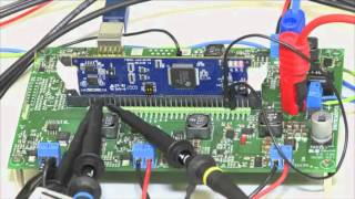
a Compensating the dead time of voltage inverters with the ADMC331 AN331-50
© Analog Devices Inc., August 2000 Page 1 of 18
a
Compensating
the dead time of
voltage inverters
with the ADMC331
AN331-50
a Compensating the dead time of voltage inverters with the ADMC331 AN331-50
© Analog Devices Inc., August 2000 Page 2 of 18
Table of Contents
SUMMARY...................................................................................................................... 3
1 DEAD TIME EFFECTS AND THEIR COMPENSATION .......................................... 3
2 IMPLEMENTATION OF THE FEED FORWARD DEAD TIME COMPENSATION .. 5
2.1 Using the dt_comp routines ...........................................................................................................................5
2.2 Using the dt_comp routine.............................................................................................................................6
2.3 The program code...........................................................................................................................................7
3 EXAMPLE: TESTING THE VALIDITY OF THE FEED FORWARD DEAD TIME
COMPENSATION........................................................................................................... 7
3.1 The construction of an inverter .....................................................................................................................7
3.2 The software program used to test the feed forward dead time compensation.........................................8
3.3 The main include file: main.h ......................................................................................................................12
3.4 The program offset.dsp and its header offset.h..........................................................................................12
3.5 Experimental results.....................................................................................................................................16
4 REFERENCES ....................................................................................................... 18
a Compensating the dead time of voltage inverters with the ADMC331 AN331-50
© Analog Devices Inc., August 2000 Page 3 of 18
Summary
Due to the finite switching time, in order to prevent the appearance of short circuits, the power devices of
an inverter must be commanded introducing a delay between their active times. This delay, called dead
time because in this period no power device is active, introduces small voltage errors, which are sufficient
to produce distorted motor currents, oscillations of the motor torque and therefore even the motor
controllability may be lost [1].
This paper presents one method to compensate the effects of the dead time, the experimental hardware on
which this method was tested and the assembly program associated with it.
1 Dead Time effects and their compensation
Consider a voltage inverter with a motor connected at its output terminals (Figure 1).
d V
T1
T 2
T 3
T 4
T 5
T 6
D1
D2 D4 D6
D3 D5
0 1 ≥ s i
1 v
Figure 1: Voltage source inverter
The effects of the dead time may be examined by considering only the first phase of the inverter. On this
phase it is desired to obtain the reference PWM signal *
1 v presented in Figure 2a. The signals used to
command the power devices are assumed to be active LOW, which means that when they are LOW, the
power devices conduct (Figures 2b and 2c). The output signal obtained at the motor terminal depends on
the sense of the current flowing in this phase:
In the case of the current flowing from inverter to the motor (assumed positive sense), when T2 conducts,
the phase terminal is linked to the GND and the voltage 1 v is 0. During the dead time period, when both
power devices are turned OFF, the current continues to flow into the motor using the reverse recovery
diode D2, so 1 v will continue to be 0. When the upper power device T1 conducts, the phase terminal is
connected to d V and 1 v is equal to d V . During the second half cycle, the phenomenon repeats itself
a Compensating the dead time of voltage inverters with the ADMC331 AN331-50
© Analog Devices Inc., August 2000 Page 4 of 18
symmetrically. The final behaviour of 1 v is presented in Figure 2d. It may be observed that the average
value of 1 v is less than the reference value by an amount determined by the dead time:
d
s
V
T
DT
v = v − ⋅ *
1 1 (1)
DT DT 2 DT 2
s T
*
1 v
T1
T 2
0
1
1
≥ s i
v when
0
1
1
< s i
v when
a)
b)
c)
d)
e)
d V
d V
*
1 T
Figure 2: The influence of the dead time over the output phase voltage
In the case of the current flowing from the motor to the inverter, when T2 conducts, the phase terminal is
linked to the GND and the voltage 1 v is 0. During the dead time period, the current continues to flow from
the motor using the reverse recovery diode D1, so 1 v will become equal to d V . When the upper power
device T1 conducts, the phase terminal is connected to d V and 1 v will continue to be equal to d V . During
the second half, the phenomenon repeats itself symmetrically. The final behaviour of 1 v is presented in
Figure 2e. It may be observed that the average value of 1 v is greater than the reference value by an
amount determined by the dead time:
a Compensating the dead time of voltage inverters with the ADMC331 AN331-50
© Analog Devices Inc., August 2000 Page 5 of 18
d
s
V
T
DT
v = v + ⋅ *
1 1 (2)
Equations (1) and (2) provide the first method to compensate for the dead time: the feed-forward
compensation. In relation of the current sense, the inverter phase will be commanded with a reference
voltage **
1 v such that the voltage 1 v at the inverter terminal will become equal with the reference voltage
*
1 v :
d
s
V
T
DT
v = v + ⋅ *
1
**
1 when i ≥ 0 (3)
d
s
V
T
DT
v = v − ⋅ *
1
**
1 when i < 0 .
These expressions mean that when the phase current is positive, the duty cycle *
1 T correspondent to *
1 v
has to be increased by the dead time and when the phase current is negative, the duty cycle has to be
decreased by the dead time. The only drawback of this method appears when the current changes its sign,
because this moment cannot be foreseen. It is easily seen that when the sign is not correctly applied, an
error of two times the dead time is introduced.
Another method to compensate the dead time is the following: The actual inverter voltages are measured
on every phase. The compensation is done adding to the reference phase voltage *
1 v a term proportional
to the voltage error on that phase:
( 1) ( 1) [ ( ) ( )] 1
*
1
*
1
**
1 v k + = v k + + K ⋅ v k − v k (4)
where:
- ** ( 1)
1 v k + is the voltage which will be commanded on the first inverter phase;
- * ( 1)
1 v k + is the reference voltage which would have been commanded if the dead time
compensation had not been considered;
-K is the gain of the compensator, usually less than or equal to 1;
- * ( )
1 v k is the reference voltage which would have been commanded during the previous PWM
cycle if the dead time compensation had not been considered;
- ( ) 1 v k is the inverter phase voltage measured during the previous PWM cycle.
The drawback of this method is that all the inverter phase voltages have to be measured. It is possible to
measure only two inverter phases if the PWM modulation is space vector type or sinusoidal.
2 Implementation of the feed forward dead time compensation
2.1 Using the dt_comp routines
The routines are developed as an easy-to-use library, which has to be linked to the user’s application. The
library consists of two files. The file “dt_comp.dsp” contains the assembly code of the subroutines. The
block has to be compiled and then linked to an application. The user has to include the header file
dt_comp.h, which provides the function-like calls to the subroutines. The example file in Section 3 will
demonstrate the usage of all the routines.
a Compensating the dead time of voltage inverters with the ADMC331 AN331-50
© Analog Devices Inc., August 2000 Page 6 of 18
Operation Usage
Compute On-times compensating the
dead time
DeadTime_Comp(StatorCurrent_struct, Dutycycles_struct)
Table 1 Implemented routine
The input vector StatorCurrents_struct consists of three elements, the three inverter phase currents.
Because their sum is always zero, only two of them need to be measured. They have to be scaled because
the DSP uses fixed point formats. The scaling factor is 2⋅ Imax , where max I represents the maximum
current which may be placed at the input pin of the A/D converter. The 2 factor is used to prevent
overflows when the currents are used in arithmetical operations.
The vector Dutycycles_struct is an input and also an output: It represents the duty cycles for each phase,
previously computed by the PWM modulator. After the compensation, they represent the duty cycles
effectively commanded to the inverter. Their values have to be between 0 and PWMTM, the number
which controls the PWM switching frequency.
DeadTime_comp represents a macro, which must be introduced into the program code if the dead time
compensation is desired. The format of inputs and outputs are explained in more detail in the next section.
The routines do not require any configuration constants from the main include-file “main.h” that comes
with every application note. For more information about the general structure of the application notes and
including libraries into user applications refer to the Library Documentation File. Section 2.2 shows an
example of usage of this library. In the following sections each routine is explained in detail with the
relevant segments of code which is found in either “dt_comp.h” or “dt_comp.dsp”. For more information
see the comments in those files.
2.2 Using the dt_comp routine
The macro listed in the Table 1 is based on a subroutine called DeadTime_Comp_. It is described in
detail in the next section. The following table gives an overview of what DSP registers are used in this
macro:
Macro Input1 and modified DAG
registers
Output2 Modified core registers
DeadTime_Comp I1 = ^ StatorCurrents_struct;
M1, M2 = 1; L1, L2 = 0;
I2 = ^ Dutycycles_struct; M3 = 0;
N/A AX0, AY0, AY1, MR,
AR
Table2. DSP core registers used in the macro
This macro has to be placed in the main program after the PWM reference duty cycles are computed, but
prior to the program that saves them into the duty cycle registers PWMCHA, PWMCHB, PWMCHC.
1 ^vector stands for ‘address of vector’.
2 N/A: The output values are stored in the output vector in the Data memory. No DSP core register is
used.
a Compensating the dead time of voltage inverters with the ADMC331 AN331-50
© Analog Devices Inc., August 2000 Page 7 of 18
2.3 The program code
The following code contained in the file dt_comp.dsp describes the routine DeadTime_Comp_
mentioned in the previous section.
The routine is organised as a loop managed by the loop counter cntr. At each iteration, one phase current
from the buffer StatorCurrents_struct is tested and the compensation is done function of its sign. In the end, the new
duty cycle number is tested to ensure it is positive and less than the maximum admissible value, PWMTM. The last
instruction saves the number back into the buffer Dutycycles_struct.
DeadTime_Comp_:
AY0 = DM(PWMDT); { dead time normalized }
AY1 = dm(PWMTM);
CNTR = 3;
do dead_loop until ce;
ax0 = DM(I1, M1); { ax0 = Isk, k=1,2,3 }
mr1 = DM(I2, M3); { load Ta, Tb, Tc }
AR = MR1 + AY0;
none = pass ax0; {chek sign of the currents }
IF LT AR = MR1 - AY0;
none = pass AR;
if lt AR = PASS 0; { no negative values admitted}
af = AR - AY1;
if gt ar = pass ay1; { protection against overflows}
dead_loop:
DM(I2, M2) = ar;
rts;
3 Example: Testing the validity of the feed forward dead time
compensation
3.1 The construction of the inverter
The proposed compensation method was implemented on the ADMC331 Processor Board mounted on
an ADMC Connector Board. As inverter power part was used an evaluation platform produced by
International Rectifier, IRPT2056D Driver-Plus Board. It is a three phase 230VAC 3HP board and it
integrates all the processing components needed for a 3 HP motor drive. It is equipped with an
IRPT2056A IGBT power module and an IR2133J driver. The Analog Devices’ ADMC PWM isolation
board linked the Connector Board to the Power Board. This board produces an electric isolation between
the digital part and the inverter power part and also inverts the signals used to drive the power devices
(74HC240). Because the signals used by the driver IR2133J are active LOW and because of the inverting
line driver HC240, the PWM outputs of the ADMC331 are set to be active HIGH. Therefore the jumper
JP51 is in position 1-2.
1 See the ADMC331 Processor Board manual, Motion Control Group, Analog Devices, 1998
a Compensating the dead time of voltage inverters with the ADMC331 AN331-50
© Analog Devices Inc., August 2000 Page 8 of 18
The inverter is driving an induction motor with the following characteristics: .13HP, 230V, 60Hz,
1725rpm, produced by Baldor. Because the power part is supplied with 110V, the maximum frequency
the motor may be run in the constant torque regime is:
c f
3
110 2
60
3
230 2 ⋅
=
⋅
f Hz c 28.7
230
110 60 = ⋅ =
Because the compensation needs the value of the inverter phase currents, two of them were sensed using
current transducers HA 10-NP produced by LEM. They are capable to measure up to 20A and this value
is used to scale down the measured values: I 20A max = . Also, an operational amplifier LM348 is used to
obtain the signal into the range of A/D converter of ADMC331: 0.3V÷3.5V. On the ADMC331 Processor
Board there are 5KHz filters that have an anti-aliasing role.
A block structure of the inverter is presented in Figure 3.
ADMCConnector Board
ADMC331 Processor
Board
IRPT2056D Driver Plus Board
ADMC PWM
Isolation Board
.13HP Induction
Motor
2xHP10-NP
s1 I
s 2 I
Figure 3. Inverter Block structure
3.2 The software program used to test the feed forward dead time compensation
The purpose of this program is to demonstrate the improvement offered by the feed forward dead time
compensation. It reads two motor currents, commands the motor to run at 14Hz, half of the cut frequency
c f and compensates for the dead time.
The file main.dsp contains the root program. The batch file build.bat compiles every file of the project,
links them together and builds the executable file main.exe. It may be applied either within DOS prompt
or clicking on it from Windows Explorer. Main.exe may be run on the Motion Control Debugger.
A brief description of the program will be given in the following:
Start of code - declaring start location in program memory
.MODULE/RAM/SEG=USER_PM1/ABS=0x30 Main_Program;
a Compensating the dead time of voltage inverters with the ADMC331 AN331-50
© Analog Devices Inc., August 2000 Page 9 of 18
Next, the general systems constants and PWM configuration constants (main.h – see the next section) are
included. Also included are the PWM library2, the DAC interface3 and the space vector modulation4 module
definitions. The header file offset.h declares some macros used to measure the offset introduced by the current
transducers and autocal.h declares the macros used to calibrate the ADMC331 A/D converter.
{***************************************************************************************
* Include General System Parameters and Libraries *
***************************************************************************************}
#include ;
#include ;
#include ;
#include ;
#include ;
#include ;
#include ;
#include ;
#include ; { Application Specific Module }
#include ;
#include ;
#include ;
Constants used in this program
{***************************************************************************************
* Constants Defined in the Module *
***************************************************************************************}
.CONST CUT_FREQ = 28; {the cutting frequency of the tested motor}
.CONST Delta = 32768*2*CUT_FREQ/PWM_freq; {the increment of the angle}
.CONST TwoPiOverThree = 0xffff / 3; { Hex equivalent of 2pi/3 }
.CONST ALLOFF = 0x3F; { Used to disable IGBTies into PWMSEG }
Here is where all the vectors for the program are declared. The buffer StatorCurrents_struct represents
the three stator currents. The PWM duty cycles are stored in the buffer Dutycycles_struct and they are initialised
with 0.It may be seen that the variables which identify the current offsets, Is1Offset and Is2Offset are declared
circular because programming becomes easier. The average of the readings is computed on 32bit precision, so
every buffer consists of 2 words.
{***************************************************************************************
* Local Variables Defined in this Module *
***************************************************************************************}
.VAR/DM/RAM/SEG=USER_DM AD_IN; { Volts/Hertz Command (0-1) }
2 see AN331-03: Three-Phase Sine-Wave Generation using the PWM Unit of the ADMC331
3 see AN331-06: Using the Serial Digital to Analog Converter of the ADMC Connector Board
4 see AN331-17: Implementing Space Vector Modulation with the ADMC331
a Compensating the dead time of voltage inverters with the ADMC331 AN331-50
© Analog Devices Inc., August 2000 Page 10 of 18
.INIT AD_IN : 0x3A0A; { Corresponds to 0.906/2 }
.VAR/DM/RAM/SEG=USER_DM Theta; { Current angle }
.INIT Theta : 0x0000;
.VAR/DM/RAM/SEG=USER_DM Vdq_ref[2]; { rotor ref.frame }
.VAR/DM/RAM/CIRC/SEG=USER_DM Valphabeta_ref[2]; { alphabeta frame }
.VAR/RAM/DM/SEG=USER_DM OnTime_struct[1*4];
.INIT OnTime_struct: 0x0000, 0x0000, 0x0000, 0x0000;
.VAR/RAM/DM/SEG=USER_DM Dutycycles_struct[1*3];
.INIT Dutycycles_struct: 0x0000, 0x0000, 0x0000;
.VAR/DM/RAM/SEG=USER_DM VrefA; { Voltage demands }
.VAR/DM/RAM/SEG=USER_DM VrefB;
.VAR/DM/RAM/SEG=USER_DM VrefC;
.INIT VrefA : 0x0000;
.INIT VrefB : 0x0000;
.INIT VrefC : 0x0000;
.VAR/DM/RAM/SEG=USER_DM StatorCurrents_struct[1*3]; { stator currents }
.VAR/DM/RAM/SEG=USER_DM Is1Offset[1];
.VAR/DM/RAM/SEG=USER_DM Is2Offset[1];
When the program begins, the PWM output signals are disabled. Then, the power module is reset and the
PWM block is set up to generate interrupts every 100μsec (see main.h in the next section). There is initialised the
D/A serial converter1 and there is unmasked the IRQ2 interrupt (the interrupt which manages the peripheral
interrupts on ADMC331). The main loop just waits for interrupts.
{********************************************************************************************}
{ Start of program code }
{********************************************************************************************}
Startup:
Write_DM(PWMSEG, ALLOFF); { the IGBTies are disabled }
IR_reset_PIO3; { Reset PowIRTrain Module }
PWM_Init(PWMSYNC_ISR, PWMTRIP_ISR);
DAC_Init; { Initialize the DAC-Module }
IFC = 0x80; { Clear any pending IRQ2 inter. }
ay0 = 0x200; { unmask irq2 interrupts. }
ar = IMASK;
ar = ar or ay0;
1 See ADMC Connector board user’s manual for further details
a Compensating the dead time of voltage inverters with the ADMC331 AN331-50
© Analog Devices Inc., August 2000 Page 11 of 18
IMASK = ar; { IRQ2 ints fully enabled here }
ADC_Init; { ADC Counter will Operate at the DSP CLKOUT Frequency }
AutoCal_Init; { Initialize the Auto Calibration Routine }
Offset_Init; { offset.h }
Main: { Wait for interrupt to occur }
jump Main;
During the PWM_SYNC interrupt there are executed some routines which determine the internal offset of
the A/D converter1, the external offsets introduced by the current transducers and the measurement of the currents.
The successive routines generate three PWM signals of 14Hz obtained applying a continuous space vector
modulation2. The dead time compensation is placed at the end of this block. Finally, the signals that will be provided
to the D/A converter are computed.
{********************************************************************************************}
{ PWM Interrupt Service Routine }
{********************************************************************************************}
PWMSYNC_ISR:
Auto_Calibrate; { autocal.h }
OffsetDetermination(ADC1, ADC2, Is1Offset, Is2Offset); { offset.h }
ReadCurrents(Is1Offset, Is2Offset, StatorCurrents_struct, ADC1, ADC2); { offset.h }
DAC_Pause; { Required only when I1, M1 or L1 is used}
ar = DM (AD_IN );
mr = 0; {Clear mr }
mr1 = dm(Theta); {Preload Theta}
my0 = Delta;
mr = mr + ar*my0 (SS); {Compute new angle & store}
dm(Theta) = mr1;
DM(Vdq_ref )= ar; {Set constant Vdq reference (AD_IN,0)}
ar = pass 0;
DM(Vdq_ref+1)= ar;
refframe_Set_DAG_registers_for_transformations;
refframe_Forward_Park_angle(Vdq_ref,Valphabeta_ref,mr1); {generate Vreference in alpha-beta frame}
SVPWM_Calc_Ontimes(Valphabeta_ref, OnTime_struct); { use SVPWM routines}
SVPWM_Calc_Dutycycles(OnTime_struct, Dutycycles_struct);
DeadTime_Comp(StatorCurrents_struct, Dutycycles_struct);
SVPWM_Update_DutyCycles(Dutycycles_struct);
Dac_Resume;
my0 = DM(Theta); DAC_Put(1, my0); { output on DACs, amplified by multiplication }
mx0 = 0x8;
my0 = DM(Dutycycles_struct ); mr = mx0 * my0 (SS); Dac_Put(2, mr0);
my0 = DM(Dutycycles_struct+1); mr = mx0 * my0 (SS); Dac_Put(3, mr0);
1 See AN331-05: ADC-system on the ADMC331.
2 See AN331-17: Implementing Space Vector Modulation with ADMC331
a Compensating the dead time of voltage inverters with the ADMC331 AN331-50
© Analog Devices Inc., August 2000 Page 12 of 18
AX0 = dm(Dutycycles_struct);
AY0 = Half_PWMTM;
AR = AX0 - AY0;
MY0 = 0x6523; {2/PWMTM=2/1296*2^15/2^6*2^15}
MR = AR * MY0 (SS);
SR = ASHIFT MR1 BY 6 (HI);
SR = SR OR LSHIFT MR0 BY 6 (LO);
DAC_Put(4, SR1);
sr1 = DM(StatorCurrents_struct); sr = ASHIFT sr1 BY 5 (HI); DAC_Put(5,sr1);
sr1 = DM(StatorCurrents_struct+1); sr = ASHIFT sr1 BY 5 (HI); DAC_Put(6, sr1);
SR1 = DM(StatorCurrents_struct+2); sr = ASHIFT sr1 BY 5 (HI); DAC_Put(7, sr1);
DAC_Update;
RTI;
3.3 The main include file: main.h
This file contains the definitions of ADMC331 constants, general-purpose macros, the configuration
parameters of the system and library routines. It should be included in every application. For more
information refer to the Library Documentation File.
This file is mostly self-explaining. As already mentioned, the dt_comp library does not require any
configuration parameters. The following table presents the parameters used to initialise the PWM block .It may be
emphasized the dead time period set at 6μsec, a large value for the power devices used on the IRPT2056D.
{********************************************************************************************}
{ Library: PWM block }
{ file : PWM331.dsp }
{ Application Note: Usage of the ADMC331 Pulse Width Modulation Block }
.CONST PWM_freq = 10000; {Desired PWM switching frequency [Hz] }
.CONST PWM_deadtime = 6000; {Desired deadtime [nsec] }
.CONST PWM_minpulse = 1000; {Desired minimal pulse time [nsec] }
.CONST PWM_syncpulse = 1540; {Desired sync pulse time [nsec] }
.CONST Half_PWMTM = 1000*Cry_clock/PWM_freq/2;
{********************************************************************************************}
3.4 The program offset.dsp and its header offset.h
The current transducers introduce an offset that has to be evaluated, otherwise the sign of the currents
would be determined with large errors. For this reason, at the beginning of the program, for a certain
number of PWM cycles (in this particular case 128, but may be more or less depending on the system)
there are measured the A/D channels corresponding to the two phase currents, V1 and V2. The average of
all measurements constitutes the offset of that current. Of course, this procedure may be applied at every
channel, if the signal is zero at the beginning of the program.
The header file offset.h contains the macros that are used during this process. Generally, they call
subroutines presented in the file offset.dsp.
This file begins declaring the variables OffsetCounter, TempOffset1 and TempOffset2 used in these
routines.
a Compensating the dead time of voltage inverters with the ADMC331 AN331-50
© Analog Devices Inc., August 2000 Page 13 of 18
{***************************************************************************************
* Global Variables Defined in this Module *
***************************************************************************************}
.VAR/DM/RAM/SEG=USER_DM OffsetCounter[1];
.GLOBAL OffsetCounter;
.VAR/DM/RAM/CIRC/SEG=USER_DM TempOffset1[2];
.GLOBAL TempOffset1;
.VAR/DM/RAM/CIRC/SEG=USER_DM TempOffset2[2];
.GLOBAL TempOffset2;
The subroutine Offset_Init_ initialises the variables used to evaluate the offsets of the current transducers.
OffsetCounter is set to 128 because the offsets are considered the average of 128 measurements.
{*************************************************************************************
* Type: Routine *
* Call: Call Offset_Init_; *
* This subroutine initializes the variables initializes variables used to *
* evaluate the offsets of the current sensors *
* Inputs : None *
* Ouputs :None *
* Modified: AR *
***************************************************************************************}
Offset_Init_:
AR = Offset_Average;
dm(OffsetCounter) = AR;
AR = 0x0;
dm(TempOffset1) = AR;
dm(TempOffset1+1) = AR;
dm(TempOffset2) = AR;
dm(TempOffset2+1) = AR;
rts;
The subroutine EvaluateIs_offset_ computes the average of the measurements of a particular A/D channel.
{***************************************************************************************
* Type: Routine *
* Call: Call EvaluateIs_offset_; *
* This subroutine computes the average of the measurements of one A/D channel *
* Inputs : AR = the lecture of the A/D channel
* I1 = placed at the begining of the buffer which is averaged *
* M1 = 0, L1 = 0 *
* Ouputs :None *
* Modified: AY1, AY0, AR, SR, AX0 *
***************************************************************************************}
EvaluateIs_offset_:
AY1 = dm(I1, M1);
a Compensating the dead time of voltage inverters with the ADMC331 AN331-50
© Analog Devices Inc., August 2000 Page 14 of 18
AY0 = dm(I1, M1);
AR = 0x4000 - AR;
SR = ASHIFT AR BY -7 (HI);
AR = SR0 + AY0;
AX0 = AR, AR = SR1 + AY1 + C;
dm(I1, M1) = AR;
dm(I1, M1) = AX0;
RTS;
. In the file offset.h there is a macro Offset_Init that initialises the address generators at the current offsets
buffers and then calls the subroutine Offset_Init_ from offset.dsp.
{***************************************************************************************
* Type: Macro *
* Call: Offset_Init; *
* This macro initializes variables used to evaluate the offsets of the current sensors *
* Input: none *
* Output: none *
* Modified: AR *
***************************************************************************************}
.MACRO Offset_Init;
CALL Offset_Init_;
.ENDMACRO;
The macro EvaluateIs_offset reads one A/D channel and computes the average offset of that channel
calling the subroutine EvaluateIs_offset_.
{***************************************************************************************
* Type: Macro *
* Call: EvaluateIs_offset; *
* Routine to compute the offset of one phase *
* Input: %0=the targeted AD channel *
* %1=the offset structure dedicated to the phase *
* %1=most significant word *
* %1+1=less significant word *
* Output: Current Offset structure *
* Modified: *
***************************************************************************************}
.MACRO EvaluateIs_offset(%0, %1);
ADC_Read(%0);
I1 = ^%1;
M1 = 1;
L1 = %%1;
a Compensating the dead time of voltage inverters with the ADMC331 AN331-50
© Analog Devices Inc., August 2000 Page 15 of 18
CALL EvaluateIs_offset_;
.ENDMACRO;
The macro OffsetDetermination computes the offsets of the both A/D channels that measure the phase
currents.
{***************************************************************************************
* Type: Macro *
* Call: OffsetDetermination *
* Routine to compute the offsets introduced by the current sensors *
* Input: %0=ADC1 *
* %1=ADC2 *
* %2=Is1Offset *
* %3=Is2Offset *
* Output: Current Offsets structure *
* Modified: *
***************************************************************************************}
.MACRO OffsetDetermination(%0, %1, %2, %3);
AY0 = dm(OffsetCounter);
AR = AY0 - 1;
IF LT JUMP SaveOffsets;
dm(OffsetCounter) = AR;
EvaluateIs_offset(%0, TempOffset1);
EvaluateIs_offset(%1, TempOffset2);
RTI;
SaveOffsets:
AF = AR + 1;
IF NE JUMP ExitOffsetDet;
dm(OffsetCounter) = AR;
AR = dm(TempOffset1);
dm(%2) = AR;
AR = dm(TempOffset2);
dm(%3) = AR;
ExitOffsetDet:
.ENDMACRO;
The macro ReadCurrents reads the two phase currents, corrects them with the offset and finally computes
the third phase current. It may be noted that the output of the A/D converter is always a positive number. Because of
the presence of an inverting operational amplifier in the hardware, in order to obtain values between –1/2 and +1/2
(in fixed point the currents are scaled by 2⋅ Imax ) the outputs of the A/D converter have to be offset by 1/2
(0x4000).
{***************************************************************************************
* Type: Macro *
* Call: ReadCurrents; *
a Compensating the dead time of voltage inverters with the ADMC331 AN331-50
© Analog Devices Inc., August 2000 Page 16 of 18
* This macro reads ADC1(Is1), ADC2(Is2) and then evaluates Is1, Is2 and Is3 *
* Input: %0 = offset of the first phase current *
* %1 = offset of the second phase current *
* %2 = the buffer of the 3 phase currents *
* %3 = ADC1 *
* %4 = ADC2 *
* Output: none *
* Modified: AY0, AR, MY0, MR, SR ,AF *
***************************************************************************************}
.MACRO ReadCurrents(%0, %1, %2, %3, %4);
ADC_Read(%3); { read Is1/Imax }
AR = 0x4000 - AR;
AY0 = dm(%0);
AR = AR - AY0;
dm(%2) = AR; { Is1/2Imax }
ADC_Read(%4); { read Is2/Imax }
AR = 0x4000 - AR;
AY0 = dm(%1);
AR = AR - AY0;
dm(%2+1) = AR; { Is2/2Imax }
AR = -AR;
AY0 = dm(%2); { Is1/2Imax }
AR = AR - AY0;
dm(%2+2) = AR; { Is3/2Imax=-Is2/2Imax-Is1/2Imax}
.ENDMACRO;
3.5 Experimental results
First of all, experiments without the dead time compensation were made. Figure 4 represents the inverter
phase voltage compared to the reference voltage that is desired at the inverter terminal and the phase
current. It may be seen that the behavior presented in chapter 1 is verified in practice: When the phase
current is positive, the real inverter phase voltage is less than the commanded one by an amount
determined by the dead time and when the phase current is negative, the real inverter phase voltage is
greater than the commanded.
At last, Figure 5 displays the inverter phase voltage and the phase current obtained with the feed forward
dead time compensation. It may be observed that the voltage still presents some distortions caused by the
nature of feed forwarding: it is supposed that the current measured during the previous PWM cycle
maintains its sign into the next PWM cycle; when the current changes the sign, this moment cannot be
foreseen and the error is doubled. These voltage deformations cause also deformations in the current
behaviour, and they may be prevented only implementing current controllers in a more accurate control
strategy, like field-oriented control.
a Compensating the dead time of voltage inverters with the ADMC331 AN331-50
© Analog Devices Inc., August 2000 Page 17 of 18
Figure 4. Reference and real inverter phase voltages and the phase current
a Compensating the dead time of voltage inverters with the ADMC331 AN331-50
© Analog Devices Inc., August 2000 Page 18 of 18
Figure 5. Inverter phase voltage and phase current after the dead time compensation
4 References
[1] Pulse dead time compensator for PWM voltage inverters, David Leggate, Russel J. Kerkman,
Industrial Electronics, Control, and Instrumentation, 1995, Proceedings of the 1995 IEEE IECON 21st
International Conference on Volume: 1, Page(s): 474 -481 vol.1.
SN74HC4066
QUADRUPLE BILATERAL ANALOG SWITCH
SCLS325G – MARCH 1996 – REVISED JULY 2003
POST OFFICE BOX 655303 • DALLAS, TEXAS 75265 1
Wide Operating Voltage Range of 2 V to 6 V
Typical Switch Enable Time of 18 ns
Low Power Consumption, 20-μA Max ICC
Low Input Current of 1 μA Max
High Degree of Linearity
High On-Off Output-Voltage Ratio
Low Crosstalk Between Switches
Low On-State Impedance . . .
50-Ω TYP at VCC = 6 V
Individual Switch Controls
description/ordering information
The SN74HC4066 is a silicon-gate CMOS quadruple analog switch designed to handle both analog and digital
signals. Each switch permits signals with amplitudes of up to 6 V (peak) to be transmitted in either direction.
Each switch section has its own enable input control (C). A high-level voltage applied to C turns on the
associated switch section.
Applications include signal gating, chopping, modulation or demodulation (modem), and signal multiplexing for
analog-to-digital and digital-to-analog conversion systems.
ORDERING INFORMATION
TA PACKAGE† ORDERABLE
PART NUMBER
TOP-SIDE
MARKING
PDIP – N Tube of 25 SN74HC4066N SN74HC4066N
Tube of 50 SN74HC4066D
SOIC – D Reel of 2500 SN74HC4066DR HC4066
Reel of 250 SN74HC4066DT
–40°C to 85°C SOP – NS Reel of 2000 SN74HC4066NSR HC4066
SSOP – DB Reel of 2000 SN74HC4066DBR HC4066
Tube of 90 SN74HC4066PW
TSSOP – PW Reel of 2000 SN74HC4066PWR HC4066
Reel of 250 SN74HC4066PWT
† Package drawings, standard packing quantities, thermal data, symbolization, and PCB design
guidelines are available at www.ti.com/sc/package.
FUNCTION TABLE
(each switch)
INPUT
CONTROL
(C)
SWITCH
L OFF
H ON
PRODUCTION DATA information is current as of publication date. Copyright 2003, Texas Instruments Incorporated
Products conform to specifications per the terms of Texas Instruments
standard warranty. Production processing does not necessarily include
testing of all parameters.
Please be aware that an important notice concerning availability, standard warranty, and use in critical applications of
Texas Instruments semiconductor products and disclaimers thereto appears at the end of this data sheet.
1
2
3
4
5
6
7
14
13
12
11
10
9
8
1A
1B
2B
2A
2C
3C
GND
VCC
1C
4C
4A
4B
3B
3A
D, DB, N, NS, OR PW PACKAGE
(TOP VIEW)
SN74HC4066
QUADRUPLE BILATERAL ANALOG SWITCH
SCLS325G – MARCH 1996 – REVISED JULY 2003
2 POST OFFICE BOX 655303 • DALLAS, TEXAS 75265
logic diagram, each switch (positive logic)
A
VCC
VCC
B
One of Four Switches
C
absolute maximum ratings over operating free-air temperature range (unless otherwise noted)†
Supply voltage range, VCC (see Note 1) . . . . . . . . . . . . . . . . . . . . . . . . . . . . . . . . . . . . . . . . . . . . . . –0.5 V to 7 V
Control-input diode current, II (VI < 0 or VI > VCC) . . . . . . . . . . . . . . . . . . . . . . . . . . . . . . . . . . . . . . . . . . . ±20 mA
I/O port diode current, II (VI < 0 or VI/O > VCC) . . . . . . . . . . . . . . . . . . . . . . . . . . . . . . . . . . . . . . . . . . . . . . ±20 mA
On-state switch current (VI/O = 0 to VCC) . . . . . . . . . . . . . . . . . . . . . . . . . . . . . . . . . . . . . . . . . . . . . . . . . . ±25 mA
Continuous current through VCC or GND . . . . . . . . . . . . . . . . . . . . . . . . . . . . . . . . . . . . . . . . . . . . . . . . . . . ±50 mA
Package thermal impedance, θJA (see Note 2): D package . . . . . . . . . . . . . . . . . . . . . . . . . . . . . . . . . . . 86°C/W
DB package . . . . . . . . . . . . . . . . . . . . . . . . . . . . . . . . . 96°C/W
N package . . . . . . . . . . . . . . . . . . . . . . . . . . . . . . . . . . . 80°C/W
NS package . . . . . . . . . . . . . . . . . . . . . . . . . . . . . . . . . 76°C/W
PW package . . . . . . . . . . . . . . . . . . . . . . . . . . . . . . . . 113°C/W
Storage temperature range, Tstg . . . . . . . . . . . . . . . . . . . . . . . . . . . . . . . . . . . . . . . . . . . . . . . . . . . –65°C to 150°C
† Stresses beyond those listed under “absolute maximum ratings” may cause permanent damage to the device. These are stress ratings only, and
functional operation of the device at these or any other conditions beyond those indicated under “recommended operating conditions” is not
implied. Exposure to absolute-maximum-rated conditions for extended periods may affect device reliability.
NOTES: 1. All voltages are with respect to ground unless otherwise specified.
2. The package thermal impedance is calculated in accordance with JESD 51-7.
SN74HC4066
QUADRUPLE BILATERAL ANALOG SWITCH
SCLS325G – MARCH 1996 – REVISED JULY 2003
POST OFFICE BOX 655303 • DALLAS, TEXAS 75265 3
recommended operating conditions (see Note 3)
MIN NOM MAX UNIT
VCC Supply voltage 2† 5 6 V
VI/O I/O port voltage 0 VCC V
VCC = 2 V 1.5 VCC
VIH High-level input voltage, control inputs VCC = 4.5 V 3.15 VCC V
VCC = 6 V 4.2 VCC
VCC = 2 V 0 0.3
VIL Low-level input voltage, control inputs VCC = 4.5 V 0 0.9 V
VCC = 6 V 0 1.2
VCC = 2 V 1000
Δt/Δv Input transition rise/fall time VCC = 4.5 V 500 ns
VCC = 6 V 400
TA Operating free-air temperature –40 85 °C
† With supply voltages at or near 2 V, the analog switch on-state resistance becomes very nonlinear. It is recommended that only digital signals
be transmitted at these low supply voltages.
NOTE 3: All unused inputs of the device must be held at VCC or GND to ensure proper device operation. Refer to the TI application report,
Implications of Slow or Floating CMOS Inputs, literature number SCBA004.
electrical characteristics over recommended operating free-air temperature range (unless
otherwise noted)
PARAMETER TEST CONDITIONS V
TA = 25C
VCC MIN MAX UNIT
MIN TYP MAX
I A V 0t V
2 V 150
ron On-state switch resistance
IT = –1 mA, VI = 0 to VCC,
4.5 V 50 85 106 Ω VC = VIH (see Figure 1)
6 V 30
V V GND V V
2 V 320
ron(p) Peak on-state resistance
VI = VCC or GND, VC = VIH,
( ) 4.5 V 70 170 215 Ω IT = –1 mA
6 V 50
II Control input current VC = 0 or VCC 6 V ±0.1 ±100 ±1000 nA
Isoff Off-state switch leakage current
VI = VCC or 0, VO = VCC or 0,
VC = VIL (see Figure 2)
6 V ±0.1 ±5 μA
Ison On-state switch leakage current
VI = VCC or 0, VC = VIH
(see Figure 3)
6 V ±0.1 ±5 μA
ICC Supply current VI = 0 or VCC, IO = 0 6 V 2 20 μA
Ci Input capacitance
A or B
5 V
9
pF
C
3 10 10
Cf
Feed-through
capacitance
A to B VI = 0 0.5 pF
Co Output capacitance A or B 5 V 9 pF
SN74HC4066
QUADRUPLE BILATERAL ANALOG SWITCH
SCLS325G – MARCH 1996 – REVISED JULY 2003
4 POST OFFICE BOX 655303 • DALLAS, TEXAS 75265
switching characteristics over recommended operating free-air temperature range
PARAMETER
FROM TO TEST
VCC
TA = 25C
MIN MAX UNIT
(INPUT) (OUTPUT) CONDITIONS
MIN TYP MAX
t P ti C 50 F
2 V 10 60 75
tPLH,
Propagation
A or B B or A CL = pF
4.5 V 4 12 15 ns
tPHL
delay time
(see Figure 4)
6 V 3 10 13
t S it h RL = 1 kΩ,
2 V 70 180 225
tPZH,
tPZL
Switch
turn-on time
C A or B
CL = 50 pF 4.5 V 21 36 45 ns
L
(see Figure 5) 6 V 18 31 38
t S it h RL = 1 kΩ,
2 V 50 200 250
tPLZ,
Switch
C A or B
CL = 50 pF 4.5 V 25 40 50 ns
tPHZ
turn-off time
L
(see Figure 5) 6 V 22 34 43
Control
CL = 15 pF,
RL = 1 kΩ
2 V 15
fI
input
frequency
C A or B
kΩ,
VC = VCC or GND,
V V /2
4.5 V 30 MHz
VO = VCC/(see Figure 6) 6 V 30
Control
feed-through
C A or B
CL = 50 pF,
Rin = RL = 600 Ω,
VC = VCC or GND
4.5 V 15
mV
noise
GND,
fin = 1 MHz
(see Figure 7)
6 V 20
(rms)
operating characteristics, VCC = 4.5 V, TA = 25°C
PARAMETER TEST CONDITIONS TYP UNIT
Cpd Power dissipation capacitance per gate CL = 50 pF, f = 1 MHz 45 pF
Minimum through bandwidth, A to B or B to A† [20 log (VO/VI)] = –3 dB
CL = 50 pF,
VC = VCC
RL = 600 Ω,
(see Figure 8)
30 MHz
Crosstalk between any switches‡ CL = 10 pF,
fin = 1 MHz
RL = 50 Ω,
(see Figure 9)
45 dB
Feed through, switch off, A to B or B to A‡ CL = 50 pF,
fin = 1 MHz
RL = 600 Ω,
(see Figure 10)
42 dB
Amplitude distortion rate, A to B or B to A
CL = 50 pF,
fin = 1 kHz
RL = 10 kΩ,
(see Figure 11)
0.05%
† Adjust the input amplitude for output = 0 dBm at f = 1 MHz. Input signal must be a sine wave.
‡ Adjust the input amplitude for input = 0 dBm at f = 1 MHz. Input signal must be a sine wave.
SN74HC4066
QUADRUPLE BILATERAL ANALOG SWITCH
SCLS325G – MARCH 1996 – REVISED JULY 2003
POST OFFICE BOX 655303 • DALLAS, TEXAS 75265 5
PARAMETER MEASUREMENT INFORMATION
VCC
VI = VCC
VC = VIH
+ 1.0 mA –
VO
ron
VI–O
10–3
VI–O
VCC
GND
(ON)
V
Figure 1. On-State Resistance Test Circuit
VCC
VC = VIL
A B
VS = VA – VB
CONDITION 1: VA = 0, VB = VCC
CONDITION 2: VA = VCC, VB = 0
VCC
GND
A (OFF)
Figure 2. Off-State Switch Leakage-Current Test Circuit
SN74HC4066
QUADRUPLE BILATERAL ANALOG SWITCH
SCLS325G – MARCH 1996 – REVISED JULY 2003
6 POST OFFICE BOX 655303 • DALLAS, TEXAS 75265
PARAMETER MEASUREMENT INFORMATION
VCC
VC = VIH
A B
VCC Open
VA = VCC TO GND
VCC
GND
A (ON)
Figure 3. On-State Leakage-Current Test Circuit
VCC
VC = VIH
VI VO
50 pF
TEST CIRCUIT
tPLH tPHL
50% 50%
VCC
0 V
50% 50%
VOH
VOL
VI
A or B
VO
B or A
VOLTAGE WAVEFORMS
50 Ω
tr
90%
10%
tf
10%
90%
VCC
GND
(ON)
Figure 4. Propagation Delay Time, Signal Input to Signal Output
SN74HC4066
QUADRUPLE BILATERAL ANALOG SWITCH
SCLS325G – MARCH 1996 – REVISED JULY 2003
POST OFFICE BOX 655303 • DALLAS, TEXAS 75265 7
PARAMETER MEASUREMENT INFORMATION
CL
GND 50 pF
VCC
VI
VO
TEST CIRCUIT
tPLZ
50%
VOLTAGE WAVEFORMS
RL
1 kΩ
10%
S1
VC
50 Ω
S2
tPZH
tPHZ
50%
50%
50%
90%
tPZL
tPZH
tPLZ
tPHZ
GND
VCC
GND
VCC
TEST S1 S2
VCC
GND
VCC
GND
tPZL
50%
VCC
VO 50%
0 V
VOL
VOH
VC
(tPZL, tPZH)
(tPLZ, tPHZ)
VCC
VCC
VO
0 V
VOL
VOH
VC
VCC
0 V
VOL
VOH
VCC
0 V
VOL
VOH
Figure 5. Switching Time (tPZL, tPLZ, tPZH, tPHZ), Control to Signal Output
SN74HC4066
QUADRUPLE BILATERAL ANALOG SWITCH
SCLS325G – MARCH 1996 – REVISED JULY 2003
8 POST OFFICE BOX 655303 • DALLAS, TEXAS 75265
PARAMETER MEASUREMENT INFORMATION
VCC
GND
VO
RL
1 kΩ
CL
15 pF
VCC
VC
50 Ω
VI = VCC
VCC
VC
0 V
VCC/2
Figure 6. Control-Input Frequency
VCC
GND
VO
RL
600 Ω
CL
50 pF
VCC
VC
50 Ω
VI
VCC/2
Rin
600 Ω
VCC/2
tr tf
90%
10%
(f = 1 MHz)
tr = tf = 6 ns
90%
10%
VCC
VC
0 V
Figure 7. Control Feed-Through Noise
VO
VCC
50 Ω
fin
VCC/2
VC = VCC
0.1 μF VI VI
(VI = 0 dBm at f = 1 MHz)
VCC
GND
(ON)
RL
600 Ω
CL
50 pF
Figure 8. Minimum Through Bandwidth
SN74HC4066
QUADRUPLE BILATERAL ANALOG SWITCH
SCLS325G – MARCH 1996 – REVISED JULY 2003
POST OFFICE BOX 655303 • DALLAS, TEXAS 75265 9
PARAMETER MEASUREMENT INFORMATION
VO1
RL
600 Ω
CL
50 pF
VCC
50 Ω
fin
VCC/2
VC = VCC
0.1 μF
VI
VI
(VI = 0 dBm at f = 1 MHz)
VO2
VCC
Rin
600 Ω
VCC/2
VC = GND
Rin
600 Ω
VCC
GND
(ON)
VCC
GND
(OFF)
RL
600 Ω
CL
50 pF
Figure 9. Crosstalk Between Any Two Switches
VO
VCC
50 Ω
fin
VC = GND
0.1 μF VI VI
(VI = 0 dBm at f = 1 MHz)
VCC
GND
(OFF)
Rin
600 Ω
RL
600 Ω
CL
50 pF
VCC/2 VCC/2
Figure 10. Feed Through, Switch Off
VI
(VI = 0 dBm at f = 1 kHz)
VO
RL
10 kΩ
CL
50 pF
VCC
VCC/2
VC = VCC
10 μF
VI fin
VCC
GND
(ON)
Figure 11. Amplitude-Distortion Rate
PACKAGE OPTION ADDENDUM
www.ti.com 10-Jun-2014
Addendum-Page 1
PACKAGING INFORMATION
Orderable Device Status
(1)
Package Type Package
Drawing
Pins Package
Qty
Eco Plan
(2)
Lead/Ball Finish
(6)
MSL Peak Temp
(3)
Op Temp (°C) Device Marking
(4/5)
Samples
SN74HC4066D ACTIVE SOIC D 14 50 Green (RoHS
& no Sb/Br)
CU NIPDAU Level-1-260C-UNLIM -40 to 85 HC4066
SN74HC4066DBLE OBSOLETE SSOP DB 14 TBD Call TI Call TI -40 to 85
SN74HC4066DBR ACTIVE SSOP DB 14 2000 Green (RoHS
& no Sb/Br)
CU NIPDAU Level-1-260C-UNLIM -40 to 85 HC4066
SN74HC4066DBRE4 ACTIVE SSOP DB 14 2000 Green (RoHS
& no Sb/Br)
CU NIPDAU Level-1-260C-UNLIM -40 to 85 HC4066
SN74HC4066DG4 ACTIVE SOIC D 14 50 Green (RoHS
& no Sb/Br)
CU NIPDAU Level-1-260C-UNLIM -40 to 85 HC4066
SN74HC4066DR ACTIVE SOIC D 14 2500 Green (RoHS
& no Sb/Br)
CU NIPDAU Level-1-260C-UNLIM -40 to 85 HC4066
SN74HC4066DRE4 ACTIVE SOIC D 14 2500 Green (RoHS
& no Sb/Br)
CU NIPDAU Level-1-260C-UNLIM -40 to 85 HC4066
SN74HC4066DRG4 ACTIVE SOIC D 14 2500 Green (RoHS
& no Sb/Br)
CU NIPDAU Level-1-260C-UNLIM -40 to 85 HC4066
SN74HC4066DT ACTIVE SOIC D 14 250 Green (RoHS
& no Sb/Br)
CU NIPDAU Level-1-260C-UNLIM -40 to 85 HC4066
SN74HC4066N ACTIVE PDIP N 14 25 Pb-Free
(RoHS)
CU NIPDAU N / A for Pkg Type -40 to 85 SN74HC4066N
SN74HC4066NE4 ACTIVE PDIP N 14 25 Pb-Free
(RoHS)
CU NIPDAU N / A for Pkg Type -40 to 85 SN74HC4066N
SN74HC4066NSR ACTIVE SO NS 14 2000 Green (RoHS
& no Sb/Br)
CU NIPDAU Level-1-260C-UNLIM -40 to 85 HC4066
SN74HC4066PW ACTIVE TSSOP PW 14 90 Green (RoHS
& no Sb/Br)
CU NIPDAU Level-1-260C-UNLIM -40 to 85 HC4066
SN74HC4066PWG4 ACTIVE TSSOP PW 14 90 Green (RoHS
& no Sb/Br)
CU NIPDAU Level-1-260C-UNLIM -40 to 85 HC4066
SN74HC4066PWLE OBSOLETE TSSOP PW 14 TBD Call TI Call TI -40 to 85
SN74HC4066PWR ACTIVE TSSOP PW 14 2000 Green (RoHS
& no Sb/Br)
CU NIPDAU Level-1-260C-UNLIM -40 to 85 HC4066
SN74HC4066PWRG4 ACTIVE TSSOP PW 14 2000 Green (RoHS
& no Sb/Br)
CU NIPDAU Level-1-260C-UNLIM -40 to 85 HC4066
SN74HC4066PWT ACTIVE TSSOP PW 14 250 Green (RoHS
& no Sb/Br)
CU NIPDAU Level-1-260C-UNLIM -40 to 85 HC4066
PACKAGE OPTION ADDENDUM
www.ti.com 10-Jun-2014
Addendum-Page 2
(1) The marketing status values are defined as follows:
ACTIVE: Product device recommended for new designs.
LIFEBUY: TI has announced that the device will be discontinued, and a lifetime-buy period is in effect.
NRND: Not recommended for new designs. Device is in production to support existing customers, but TI does not recommend using this part in a new design.
PREVIEW: Device has been announced but is not in production. Samples may or may not be available.
OBSOLETE: TI has discontinued the production of the device.
(2) Eco Plan - The planned eco-friendly classification: Pb-Free (RoHS), Pb-Free (RoHS Exempt), or Green (RoHS & no Sb/Br) - please check http://www.ti.com/productcontent for the latest availability
information and additional product content details.
TBD: The Pb-Free/Green conversion plan has not been defined.
Pb-Free (RoHS): TI's terms "Lead-Free" or "Pb-Free" mean semiconductor products that are compatible with the current RoHS requirements for all 6 substances, including the requirement that
lead not exceed 0.1% by weight in homogeneous materials. Where designed to be soldered at high temperatures, TI Pb-Free products are suitable for use in specified lead-free processes.
Pb-Free (RoHS Exempt): This component has a RoHS exemption for either 1) lead-based flip-chip solder bumps used between the die and package, or 2) lead-based die adhesive used between
the die and leadframe. The component is otherwise considered Pb-Free (RoHS compatible) as defined above.
Green (RoHS & no Sb/Br): TI defines "Green" to mean Pb-Free (RoHS compatible), and free of Bromine (Br) and Antimony (Sb) based flame retardants (Br or Sb do not exceed 0.1% by weight
in homogeneous material)
(3) MSL, Peak Temp. - The Moisture Sensitivity Level rating according to the JEDEC industry standard classifications, and peak solder temperature.
(4) There may be additional marking, which relates to the logo, the lot trace code information, or the environmental category on the device.
(5) Multiple Device Markings will be inside parentheses. Only one Device Marking contained in parentheses and separated by a "~" will appear on a device. If a line is indented then it is a continuation
of the previous line and the two combined represent the entire Device Marking for that device.
(6) Lead/Ball Finish - Orderable Devices may have multiple material finish options. Finish options are separated by a vertical ruled line. Lead/Ball Finish values may wrap to two lines if the finish
value exceeds the maximum column width.
Important Information and Disclaimer:The information provided on this page represents TI's knowledge and belief as of the date that it is provided. TI bases its knowledge and belief on information
provided by third parties, and makes no representation or warranty as to the accuracy of such information. Efforts are underway to better integrate information from third parties. TI has taken and
continues to take reasonable steps to provide representative and accurate information but may not have conducted destructive testing or chemical analysis on incoming materials and chemicals.
TI and TI suppliers consider certain information to be proprietary, and thus CAS numbers and other limited information may not be available for release.
In no event shall TI's liability arising out of such information exceed the total purchase price of the TI part(s) at issue in this document sold by TI to Customer on an annual basis.
TAPE AND REEL INFORMATION
*All dimensions are nominal
Device Package
Type
Package
Drawing
Pins SPQ Reel
Diameter
(mm)
Reel
Width
W1 (mm)
A0
(mm)
B0
(mm)
K0
(mm)
P1
(mm)
W
(mm)
Pin1
Quadrant
SN74HC4066DBR SSOP DB 14 2000 330.0 16.4 8.2 6.6 2.5 12.0 16.0 Q1
SN74HC4066DR SOIC D 14 2500 330.0 16.4 6.5 9.0 2.1 8.0 16.0 Q1
SN74HC4066DT SOIC D 14 250 330.0 16.4 6.5 9.0 2.1 8.0 16.0 Q1
SN74HC4066NSR SO NS 14 2000 330.0 16.4 8.2 10.5 2.5 12.0 16.0 Q1
SN74HC4066PWR TSSOP PW 14 2000 330.0 12.4 6.9 5.6 1.6 8.0 12.0 Q1
SN74HC4066PWT TSSOP PW 14 250 330.0 12.4 6.9 5.6 1.6 8.0 12.0 Q1
PACKAGE MATERIALS INFORMATION
www.ti.com 14-Jul-2012
Pack Materials-Page 1
*All dimensions are nominal
Device Package Type Package Drawing Pins SPQ Length (mm) Width (mm) Height (mm)
SN74HC4066DBR SSOP DB 14 2000 367.0 367.0 38.0
SN74HC4066DR SOIC D 14 2500 367.0 367.0 38.0
SN74HC4066DT SOIC D 14 250 367.0 367.0 38.0
SN74HC4066NSR SO NS 14 2000 367.0 367.0 38.0
SN74HC4066PWR TSSOP PW 14 2000 367.0 367.0 35.0
SN74HC4066PWT TSSOP PW 14 250 367.0 367.0 35.0
PACKAGE MATERIALS INFORMATION
www.ti.com 14-Jul-2012
Pack Materials-Page 2
MECHANICAL DATA
MSSO002E – JANUARY 1995 – REVISED DECEMBER 2001
POST OFFICE BOX 655303 • DALLAS, TEXAS 75265
DB (R-PDSO-G**) PLASTIC SMALL-OUTLINE
4040065 /E 12/01
28 PINS SHOWN
Gage Plane
8,20
7,40
0,55
0,95
0,25
38
12,90
12,30
28
10,50
24
8,50
Seating Plane
7,90 9,90
30
10,50
9,90
0,38
5,60
5,00
15
0,22
14
A
28
1
16 20
6,50 6,50
14
0,05 MIN
5,90 5,90
DIM
A MAX
A MIN
PINS **
2,00 MAX
6,90
7,50
0,65 0,15 M
0°–�8°
0,10
0,09
0,25
NOTES: A. All linear dimensions are in millimeters.
B. This drawing is subject to change without notice.
C. Body dimensions do not include mold flash or protrusion not to exceed 0,15.
D. Falls within JEDEC MO-150
IMPORTANT NOTICE
Texas Instruments Incorporated and its subsidiaries (TI) reserve the right to make corrections, enhancements, improvements and other
changes to its semiconductor products and services per JESD46, latest issue, and to discontinue any product or service per JESD48, latest
issue. Buyers should obtain the latest relevant information before placing orders and should verify that such information is current and
complete. All semiconductor products (also referred to herein as “components”) are sold subject to TI’s terms and conditions of sale
supplied at the time of order acknowledgment.
TI warrants performance of its components to the specifications applicable at the time of sale, in accordance with the warranty in TI’s terms
and conditions of sale of semiconductor products. Testing and other quality control techniques are used to the extent TI deems necessary
to support this warranty. Except where mandated by applicable law, testing of all parameters of each component is not necessarily
performed.
TI assumes no liability for applications assistance or the design of Buyers’ products. Buyers are responsible for their products and
applications using TI components. To minimize the risks associated with Buyers’ products and applications, Buyers should provide
adequate design and operating safeguards.
TI does not warrant or represent that any license, either express or implied, is granted under any patent right, copyright, mask work right, or
other intellectual property right relating to any combination, machine, or process in which TI components or services are used. Information
published by TI regarding third-party products or services does not constitute a license to use such products or services or a warranty or
endorsement thereof. Use of such information may require a license from a third party under the patents or other intellectual property of the
third party, or a license from TI under the patents or other intellectual property of TI.
Reproduction of significant portions of TI information in TI data books or data sheets is permissible only if reproduction is without alteration
and is accompanied by all associated warranties, conditions, limitations, and notices. TI is not responsible or liable for such altered
documentation. Information of third parties may be subject to additional restrictions.
Resale of TI components or services with statements different from or beyond the parameters stated by TI for that component or service
voids all express and any implied warranties for the associated TI component or service and is an unfair and deceptive business practice.
TI is not responsible or liable for any such statements.
Buyer acknowledges and agrees that it is solely responsible for compliance with all legal, regulatory and safety-related requirements
concerning its products, and any use of TI components in its applications, notwithstanding any applications-related information or support
that may be provided by TI. Buyer represents and agrees that it has all the necessary expertise to create and implement safeguards which
anticipate dangerous consequences of failures, monitor failures and their consequences, lessen the likelihood of failures that might cause
harm and take appropriate remedial actions. Buyer will fully indemnify TI and its representatives against any damages arising out of the use
of any TI components in safety-critical applications.
In some cases, TI components may be promoted specifically to facilitate safety-related applications. With such components, TI’s goal is to
help enable customers to design and create their own end-product solutions that meet applicable functional safety standards and
requirements. Nonetheless, such components are subject to these terms.
No TI components are authorized for use in FDA Class III (or similar life-critical medical equipment) unless authorized officers of the parties
have executed a special agreement specifically governing such use.
Only those TI components which TI has specifically designated as military grade or “enhanced plastic” are designed and intended for use in
military/aerospace applications or environments. Buyer acknowledges and agrees that any military or aerospace use of TI components
which have not been so designated is solely at the Buyer's risk, and that Buyer is solely responsible for compliance with all legal and
regulatory requirements in connection with such use.
TI has specifically designated certain components as meeting ISO/TS16949 requirements, mainly for automotive use. In any case of use of
non-designated products, TI will not be responsible for any failure to meet ISO/TS16949.
Products Applications
Audio www.ti.com/audio Automotive and Transportation www.ti.com/automotive
Amplifiers amplifier.ti.com Communications and Telecom www.ti.com/communications
Data Converters dataconverter.ti.com Computers and Peripherals www.ti.com/computers
DLP® Products www.dlp.com Consumer Electronics www.ti.com/consumer-apps
DSP dsp.ti.com Energy and Lighting www.ti.com/energy
Clocks and Timers www.ti.com/clocks Industrial www.ti.com/industrial
Interface interface.ti.com Medical www.ti.com/medical
Logic logic.ti.com Security www.ti.com/security
Power Mgmt power.ti.com Space, Avionics and Defense www.ti.com/space-avionics-defense
Microcontrollers microcontroller.ti.com Video and Imaging www.ti.com/video
RFID www.ti-rfid.com
OMAP Applications Processors www.ti.com/omap TI E2E Community e2e.ti.com
Wireless Connectivity www.ti.com/wirelessconnectivity
Mailing Address: Texas Instruments, Post Office Box 655303, Dallas, Texas 75265
Copyright © 2014, Texas Instruments Incorporated
a Using a Tracebuffer with the ADMCF32X ANF32X-34
© Analog Devices Inc., March 2000 Page 1 of 11
a
Using a Tracebuffer with the
ADMCF32X
ANF32X-34
a Using a Tracebuffer with the ADMCF32X ANF32X-34
© Analog Devices Inc., March 2000 Page 2 of 11
Table of Contents
SUMMARY...................................................................................................................... 3
1 THE TRACEBUFFER STRUCTURE........................................................................ 3
1.1 The Tracebuffer Data-Array.........................................................................................................................4
2 IMPLEMENTATION OF THE TRACEBUFFER LIBRARY ROUTINES ................... 5
2.1 Usage of the tracebuffer routines ..................................................................................................................5
2.2 Usage of the DSP registers .............................................................................................................................5
2.3 Access to the library: the header file.............................................................................................................6
2.4 The program macro........................................................................................................................................7
3 SOFTWARE EXAMPLE: TRACEBUFFER.............................................................. 8
3.1 Usage of the Tracebuffer routine an example ..............................................................................................8
3.2 The main program: main.dsp........................................................................................................................8
4 EXPERIMENTAL RESULTS.................................................................................. 10
a Using a Tracebuffer with the ADMCF32X ANF32X-34
© Analog Devices Inc., March 2000 Page 3 of 11
Summary
In many cases the plotting and processing data externally are needed to verify and debug code and
structure in a DSP. This application note describe the use of a tracebuffer structure where values treated in
the DSP can be saved in a data-array and used for internal of external modification interfaced though the
Motion Control Debugger system.
1 The Tracebuffer Structure
A data-array structure is defined to enable saving arrays of values in data-memory (DM). This array of
memory locations can be addressed by the use of the pointer-system on the 2171 core. With this structure
defined, further treating or evaluation of the internal data-calculations can be analyzed and checked for
errors.
Using the Motion Control Debugger the values can be either be plotted directly or dumped for analyzing
the data-array in other external programs
In the chosen structure any number of pointer arrays in DM can be enabled and individually initialized for
locations in DM. The structure will furthermore allow the user to under-sample the writing to the buffer.
Initialize
the Tracebuffer
Though macro
Is the Sample Ratio = Sample number?
Is Flag enabled ?
Is there still space in the Buffer Full ?
YES
No
YES
No
Update Buffer and increment
pointer and counter
End Macro;
Macro Call
YES
No
Figure 1 - Flowchart for the Buffer writing
The flow chart illustrate the structure of the trace buffer writing. Initialization is done in the startup
sequence. After this, the Flag is checked - is the flag set then the corresponding tracebuffer is enabled.
Secondly the buffer is checked for available spaces. If the DM locations defined for memory write aren't
full it is safe to go on. If the buffer is full return. Finally the sample-ratio is checked. If a sample-ratio is
a Using a Tracebuffer with the ADMCF32X ANF32X-34
© Analog Devices Inc., March 2000 Page 4 of 11
declared different from zero then check if the sample-number is equal to the sample-ratio. If it is write the
chosen variable to the data-array. If not, return to the subroutine.
The structure of the buffer is circular and to optimize the flexibility the format is provided as a complete
macro setting with locked data-array format.
1.1 The Tracebuffer Data-Array
To enable the tracebuffer array in DM it is necessary to define a given circular buffer with associated
pointer. The circular buffer is structured as:
First location : Statement of flag - ON/OFF
Second location : Pointer to next free address
Third location : Sample ratio (specified by the user)
Fourth location : Sample number (used during the re-sampling of values)
Fifth location : Counter for the buffer.
Sixth to XXX locations : Placement for the values
Every time the macro is called, Ex. in the PWMSYNC_ISR, a new value is added to the buffer if there are
available space left and the sample number is equal to the under-sample ratio.
DM(Address) Flag (ON/OFF)
DM(Address+1) Pointer to next free
address
.. Sample ratio
.. Sample number
.. Counter for Buffer
.. First Data-placement
.. Value(1)
.. Value(2)
..
..
..
..
..
..
.. Value (Buffer size -2)
.. Value (Buffer size -1)
.. Value (Buffer size)
Figure 2 - Tracebuffer - locations in DM
Figure 2 illustrates how the values are placed in the allocated DM locations. Here values are stored at
specific addresses in order to analyze these off-line.
First value
Placed in the
buffer
N = numbers
in
tracebuffer
Buffer full
a Using a Tracebuffer with the ADMCF32X ANF32X-34
© Analog Devices Inc., March 2000 Page 5 of 11
2 Implementation of the Tracebuffer Library Routines
2.1 Usage of the tracebuffer routines
The routines are developed as an easy-to-use library, which has to be linked to the user’s application. The
library consists of two files. The file “T_buffer.dsp” contains the assembly code for the subroutines. This
package has to be compiled and can then be linked to an application. The user has to include the header
file “T_buffer.h”, which provides the function-like macros for this routine. The following table
summarizes the set of macros that are defined in this library.
Operation Usage Input Output
Initialization Buffer_Init("name", sample ratio);
Name &
Sample
ratio
None
Activate Buffer_ON("name"); Name None
Deactivate Buffer_OFF("name"); Name None
Record Buffer_Record("name", value);
Name &
Value
None
Table 1: Implemented routines
The four-macro settings allow the user to setup any given DM-locations for trace-buffer availability.
Specifying the selected buffer and record value enables the flexibility of writing any number to a known
position in memory.
2.2 Usage of the DSP registers
Table 2 gives an overview of the DSP core registers that are modified by the four macros mentioned
above. Obviously, also the "input" values are modified.
Usage Modified registers
Buffer_Init("name", sample ratio); ax0
Buffer_OFF("name"); ax0
Buffer_ON("name"); ax0
Buffer_Record("name", value);
ax0, ax1, ay0, ar,
I5, M5
Table 2: Usage of DSP core registers for the subroutines
a Using a Tracebuffer with the ADMCF32X ANF32X-34
© Analog Devices Inc., March 2000 Page 6 of 11
2.3 Access to the library: the header file
Including the header file "t_buffer.h" into the application code may access the library.
The header file is intended to provide function-like macros to the Trace buffer routines. It defines the calls
shown in Table 1. The file is mostly self-explaining but some comments have to be added. The sample ratio is
here defined as how often is a new value can be written to the buffer.
First macro is the Buffer_Init macro. This macro initializes the five first location of the circular buffer in
respect to "name of the buffer" and the sample-ratio. Furthermore the sample-number and the internal
counter is cleared.
The second and third macro Buffer_ON and Buffer_OFF just enables or disables writing to the buffers. In
this case the first location in the buffer ( the flag ) are set/or cleared.
{********************************************************************************
* *
* Type: Macro *
* *
* Call: Buffer_Init("Buffer", sampleratio) *
* Description : Initialize the tracebuffer *
* *
* Undersample ratio 0 = every time *
* 1 = every 1.time *
* 2 = every 2.time ..... *
* *
* Ouputs : none *
* *
* Modified: ax0 *
* *
********************************************************************************}
.MACRO Buffer_Init(%0,%1);
ax0 = %1; { Sample ratio }
dm(%0+2)= ax0;
ax0 =^%0+5; { Store start value }
dm(%0+1)= ax0; { first location for data }
ax0 = 0x0000;
dm(%0) = ax0; { Clear Flag - Non-Active }
dm(%0+3)= ax0; { Clear sample number }
dm(%0+4)= ax0; { Clear counter for this buffer }
.ENDMACRO;
{********************************************************************************
* *
* Type: Macro *
* *
* Call: Buffer_ON("buffer") *
* *
* Description : Enable tracebuffer "Buffer" *
* Ouputs : none *
* *
* Modified : ax0 *
* *
********************************************************************************}
.MACRO Buffer_ON(%0);
ax0 = 1;
dm(%0) = ax0;
.ENDMACRO;
a Using a Tracebuffer with the ADMCF32X ANF32X-34
© Analog Devices Inc., March 2000 Page 7 of 11
{********************************************************************************
* *
* Type: Macro *
* *
* Call: Buffer_OFF("buffer") *
* *
* Description : Disable tracebuffer "Buffer" *
* Ouputs : none *
* *
* Modified : ax0 *
* *
********************************************************************************}
.MACRO Buffer_OFF(%0);
ax0 = 0;
dm(%0) = ax0;
.ENDMACRO;
2.4 The program macro
The following code contained in the file “t_buffer.h” defines the macrocode used for the Tracebuffer. In
many cases this piece of code is placed in the "t_buffer.dsp"-file but here the flexibility advances by
placing the program-code directly in the macro. It should be mentioned that this way of using the
tracebuffer enables flexibility but takes up more memory.
The following code implements the tracebuffer routines. Refer to the flowchart in section 1 for the structure
of the buffers. Input to the tracebuffer are any numbers computed in the DSP.
Underneath is the code for the Buffer_Record.. It just need to be said that since the buffer is structured as a
circular buffer the data-placement for each of the "buffer-handle" values are placed from buffer-location 1 to
5 (here %0….%0+4)
{********************************************************************************
* *
* Type: Macro *
* *
* all: Buffer_Record(buffer,data) *
* *
* Description : Place data in buffer memory *
* Ouputs : none *
* *
* Modified: M5, I5, ar, ax1, ax0, ay0 *
* *
********************************************************************************}
.MACRO Buffer_Record(%0,%1);
.Local Continue1,Continue2,Continue3,End; { Local routines in Macro }
M5 = 1; { modify factor = 1 }
ax1 = %1;
I5 = ^%0; { load start value for pointer }
ar = dm(%0); { temporary storage }
ar= tstbit 0 of ar;
if NE jump Continue1;
Jump end;
Continue1:
ax0 = %%0;
ay0 = dm(%0+4);
ar = ax0 - ay0;
if gt jump Continue2;
ax0 = 0x0000;
dm(%0) = ax0;
Jump end;
a Using a Tracebuffer with the ADMCF32X ANF32X-34
© Analog Devices Inc., March 2000 Page 8 of 11
Continue2: { is sample_num equal to ratio? }
ax0 = dm(%0+3);
ay0 = dm(%0+2);
ar = ax0 - ay0;
if eq jump Continue3;
ar = ax0 + 1;
dm(%0+3) = ar;
Jump end;
Continue3: { write into buffer }
I5 = dm(%0+1); { load backup value for pointer }
dm(I5,M5) = ax1; { Value updated to Buffer }
ax0 = dm(%0+4); { increment count }
ar = ax0 + 1;
dm(%0+4) = ar;
ax0 = 0x0000; { clear sample_num }
dm(%0+3) = ax0;
dm(%0+1) = I5;
end:
.ENDMACRO;
3 Software Example: Tracebuffer
3.1 Usage of the Tracebuffer routine an example
This example demonstrates how two values are written to Buffer1 and Buffer2. In this case the memorylocations
used as buffers are set to 2*105-locations (100 location of calculated data). The values written
to these two buffer-arrays are values computed for three 120-degree phase shifted reference voltages.
3.2 The main program: main.dsp
The file “main.dsp” contains the initialisation and PWM Sync and Trip interrupt service routines. To
activate, build the executable file using the attached build.bat either within your DOS prompt or clicking
on it from Windows Explorer. This will create the object files and the main.exe example file. This file
may be run on the Motion Control Debugger. The program can be booted from Flash but in this
tracebuffer case it is not effectuated since the DM can not be read without the Motion Control Debugger.
Every module besides from the Main_program module is by default placed in either one of the three
USERFLASH memory banks.
In the following, a brief description of the code is given.
Start of code – declaring start location in program memory or FLASH memory. Comments are placed
depending on whether the program should run in PMRAM or Flash memory.
{**************************************************************************************
* Application: Starting from FLASH (out-comment the one not used)
**************************************************************************************}
!.MODULE/RAM/SEG=USERFLASH1/ABS=0x2200 Main_Program;
{**************************************************************************************
* Application: Starting from RAM (out-comment the one not used)
**************************************************************************************}
.MODULE/RAM/SEG=USER_PM1/ABS=0x30 Main_Program;
a Using a Tracebuffer with the ADMCF32X ANF32X-34
© Analog Devices Inc., March 2000 Page 9 of 11
Next, the general systems constants and PWM configuration constants (main.h – see the next section) are
included. Also included are the PWM library and the T_BUFFER library definitions
{********************************************************************************
* Include General System Parameters and Libraries *
********************************************************************************}
#include ;
#include ;
#include ;
#include ;
{********************************************************************************
* Local Variables Defined in this Module *
********************************************************************************}
.VAR/DM/RAM/SEG=USER_DM AD_IN; { Volts/Hertz Command (0-1) }
.VAR/DM/RAM/SEG=USER_DM Theta; { Current angle }
.VAR/DM/RAM/SEG=USER_DM VrefA; { Voltage demands }
.VAR/DM/RAM/SEG=USER_DM VrefB;
.VAR/DM/RAM/SEG=USER_DM VrefC;
.VAR/DM/RAM/CIRC/SEG=USER_DM Buffer1[105]; { Tracebuffer }
.VAR/DM/RAM/CIRC/SEG=USER_DM Buffer2[105]; { Tracebuffer }
ar = 0x7FFF; dm(AD_IN) = ar;
ar = 0x0000; dm(Theta) = ar; dm(VrefA) = ar; dm(VrefB) = ar; dm(VrefC) = ar;
Some Variables are defined hereafter. These are used to calculate the three reference voltages. For further
information see ANF32X-3. The two circular buffers are defined - here the size is 105 locations (5 locations
are used for handling the buffer) this number is arbitrary - just depending on the memory locations occupied
by these buffers.
The first thing that is done in the initialisation block (Startup) is checking a selected PIO line for level. If the
PIO-pin is high jump to an ERASE BOOT FROM FLASH BIT routine in ROM and return. If not, just go
ahead with normal operation. This small macro is done to enable re-coding of the FLASH memory. For
further information (See Reference Manual). In this example the PIO-pin 6 is chosen as erase pin. The
initialisation of the PWM block is executed. Note how the interrupt vectors for the PWMSync and PWMTrip
service routines are passed as arguments. Then the interrupt IRQ2 is enabled by setting the corresponding
bit in the IMASK register. Two Tracebuffers are initialised with 1x under-sampling Then the Tracebuffers
are activated by setting the flag (Buffer_ON(Buffer1) & Buffer_ON(Buffer2)). After that, the program
enters a loop, which just waits for interrupts.
{********************************************************************************
* Start of program code *
********************************************************************************}
Startup:
FLASH_erase_PIO(6); { Select PIO6 as clearing PIO }
{ Remember that sport1 is muxed with the PIO-lines }
{ If the bit is high Clear Memory and Boot from }
{ Flash bit }
PWM_Init(PWMSYNC_ISR, PWMTRIP_ISR);
IFC = 0x80; { Clear any pending IRQ2 inter. }
ay0 = 0x200; { unmask irq2 interrupts. }
ar = IMASK;
ar = ar or ay0;
IMASK = ar; { IRQ2 ints fully enabled here }
Buffer_Init(Buffer1, 1); { 1x undersampling }
Buffer_Init(Buffer2, 1); { 1X undersampling }
Buffer_ON(Buffer1); { Activate the Buffer }
Buffer_ON(Buffer2); { Activate the Buffer }
Main: { Wait for interrupt to occur }
jump Main;
rts;
a Using a Tracebuffer with the ADMCF32X ANF32X-34
© Analog Devices Inc., March 2000 Page 10 of 11
In the PWMSYNC_ISR the DAGS are first set up for trigonometric functionality. Three reference voltages
VrefA,B and C are calculated on base of the trigonometric functions in the Trigonometric-library ( See
ANF32X-10 ). The PWM block is update with these control signals and finally the two Tracebuffers Buffer1
and Buffer2 are updated. Here the variables VrefA and VrefB are stored in the two data-arrays.
PWMSYNC_ISR:
Set_DAG_registers_for_trigonometric;
my0 = DM(AD_IN);
mr = 0; { Clear mr }
mr1 = dm(Theta); { Preload Theta }
mx0 = Delta;
mr = mr + mx0*my0 (SS); { Compute new angle & store }
dm(Theta) = mr1;
Sin(mr1); { Result in ar register }
mr = ar*my0 (SS); { Multiply by Scale for VrefA }
dm(VrefA) = mr1;
ax1 = dm(Theta); { Compute angle of phase B }
ay1 = TwoPioverThree;
ar = ax1 - ay1;
Sin(ar); { Result in ar register }
mr = ar*my0 (SS); { Multiply by Scale for VrefB }
dm(VrefB) = mr1;
ax1 = dm(Theta); { Compute angle of phase C }
ay1 = TwoPioverThree;
ar = ax1 + ay1;
Sin(ar); { Result in ar register }
mr = ar*my0 (SS); { Multiply by Scale for VrefC }
dm(VrefC) = mr1;
ax0 = DM(VrefA); ax1 = DM(VrefB); ay0 = DM(VrefC); ay1= DM(Theta);
PWM_update_demanded_Voltage(ax0,ax1,ay0);
{*******************************************************************************
* Update tracebuffers *
*******************************************************************************}
ax0 = DM(VrefA); Buffer_Record(Buffer1,ax0);
ax0 = DM(VrefB); Buffer_Record(Buffer2,ax0);
RTI;
It has to be mentioned that the Buffer_Record macro uses some DSP registers (see T_buffer.h) for that
reason the proposed way of writing to the buffer is as defined above.
4 Experimental results
The experimental results illustrated beneath are two plots of VrefA and VrefB. These values are written
into Buffer1 and Buffer2 and then plotted though the Motion Control Debugger. As can be seen on Figure
3 the two waveforms are plotted as a function of the given number in Buffer1 and 2.
From the figures the scaling can also be seen - here the numbers are represented in decimal. Selecting
another scaling of these reference-voltages will re-scale these plots.
a Using a Tracebuffer with the ADMCF32X ANF32X-34
© Analog Devices Inc., March 2000 Page 11 of 11
Figure 3 - Plot from the Motion Control Debugger using the Internal Plot Function.
www.analog.com
Developing VisualAudio Modules
Copyright Information
© 2006 Analog Devices, Inc., ALL RIGHTS RESERVED. This document may not be reproduced in any form without prior, express written consent from Analog Devices, Inc.
Printed in the USA.
Disclaimer
Analog Devices, Inc. reserves the right to change this product without prior notice. Information furnished by Analog Devices is believed to be accurate and reliable. However, no responsibility is assumed by Analog Devices for its use; nor for any infringement of patents or other rights of third parties which may result from its use. No license is granted by implication or otherwise under the patent rights of Analog Devices, Inc.
Trademark and Service Mark Notice
The Analog Devices logo, VisualDSP++, VisualAudio, SHARC, Blackfin, and EZ-KIT Lite are registered trademarks of Analog Devices, Inc.
All other brand and product names are trademarks or service marks of their respective owners.
2 of 51
Contents
Contents..............................................................................................................................................................................................................3
Preface.................................................................................................................................................................................................................4
Purpose of This Manual................................................................................................................................................................................4
Custom Audio Modules....................................................................................................................................................................................5
Overview.........................................................................................................................................................................................................5
Numerics on the Blackfin and SHARC.......................................................................................................................................................9
Example 1A – Mono Parametric Scaling....................................................................................................................................................9
Example 1B – Render Function in ASM.................................................................................................................................................19
Scratch Buffers............................................................................................................................................................................................22
Auxiliary Memory for Module Instances................................................................................................................................................22
Pointer Aliasing Rules................................................................................................................................................................................25
Meta-Variables and Expressions...............................................................................................................................................................26
Modifying Module Parameters.................................................................................................................................................................27
Expression Language Details.....................................................................................................................................................................28
Modules With Data of Varying Size.........................................................................................................................................................33
Modules With a Variable Number of Pins...............................................................................................................................................34
Frequency Domain Processing.................................................................................................................................................................36
Other Features of the XML File................................................................................................................................................................36
Custom Bypass Functions..........................................................................................................................................................................38
SHARC SIMD Considerations..................................................................................................................................................................38
Adjusting Modules from Other Modules................................................................................................................................................39
Dynamically Changing a Module’s Render Function............................................................................................................................39
Compatibility between Blackfin and SHARC Modules.........................................................................................................................39
Reference Section............................................................................................................................................................................................41
AudioProcessing.h Structures...................................................................................................................................................................41
Module Memory Sections.........................................................................................................................................................................44
Summary of Naming Conventions...........................................................................................................................................................45
Inspector Control Types............................................................................................................................................................................47
XML Format................................................................................................................................................................................................50
Index.................................................................................................................................................................................................................51
3 of 51
Preface
PURPOSE OF THIS MANUAL
The VisualAudio Designer Users’ Guide explains how to use VisualAudio to develop audio processing software for a wide variety of products. The guide describes the graphical interface, provides step-by-step procedures for completing tasks, and contains detailed technical information on how to integrate the generated code into your final product.
Intended Audience
The primary audience for this manual is a programmer who is familiar with Analog Devices, Inc. processors. This manual assumes that the audience can use the VisualDSP++ development environment to develop, build, and debug Digital Signal Processing (DSP) applications for the SHARC or Blackfin processor. 4 of 51
Custom Audio Modules
This document explains how to write an audio processing module for VisualAudio for SHARC processors in the 26x and 36x families, as well as for Blackfin processors in the 53x and 56x families.
Audio modules allow audio processing (sometimes called “post-processing”) to be implemented by making use of a number of smaller, self-contained processing blocks.
The topics are organized as follows.
• “Overview”
• “Numerics on SHARC and Blackfin”
• “Example 1A – Mono parameter scaling”
• “Example 1B – Render function in ASM”
• “Scratch Buffers”
• “Auxiliary Memory for Module Instances”
• “Pointer Aliasing Rules”
• “Meta-variables and Expressions”
• “Modifying Module Parameters”
• “Expression Language Details”
• “Modules with Data of Varying Size”
• “Modules with Variable Numbers of Pins”
• “Other Features of the XML File”
• Custom Bypass Functions”
• “SHARC SIMD Considerations”
• “Adjusting Modules from Other Modules”
• “Dynamically Changing a Module’s Render Function”
• “Compatibility between Blackfin and SHARC Modules”
OVERVIEW
This section includes a brief philosophical review of what motivated certain design decisions, a discussion about the quasi-object orientation inherent in the module concept, a description of usage scenarios and a high-level description of the parts of a module.
Design Philosophy
The module format was designed with the following goals in mind.
• Minimal run-time processor footprint
• CPU efficiency
• Straightforward to write and use
Several key features help accomplish these goals.
• VisualAudio does as much work as possible at compile and assembly time to enable the production DSP code to be lean, while still providing a flexible environment for creating and deploying modules.
• Modules process a block of samples at a time to ensure that the cost of loading and storing state and parameters is incurred only once per block instead of once per sample.
• VisualAudio supports interleaved stereo connections between modules to enable a common use of Single-Instruction, Multiple-Data (SIMD) on the SHARC DSP. This signal type is also supported on the Blackfin, primarily for compatibility with system designs originating on SHARCs.
5 of 51
• VisualAudio supports signals at both the audio sampling rate and a lower “control rate.” This allows slowly-changing control signals to use less memory and MIPS.
• VisualAudio supports a variety of frequency domain signal types, as well as a user-settable FFT size and hop factor for “overlap-add” and “overlap-save” style processing.
• Some of the spirit of object-oriented programming is borrowed, while a lean approach is maintained. Note that C++ is not used.
• To keep the CPU usage (MIPS) of a module relatively constant, a module instance should perform roughly the same operations every time it runs. Assume the module’s worst case CPU usage. The exception is when there are clear modes. In this case, the user can plan in advance the combination of module modes that will be in use at a particular time.
• In keeping with the goals of near-constant CPU usage and minimal memory usage, parameter calculation (such as filter design) is normally pushed forward to design time, and implemented outside the DSP runtime (for example within VisualAudio Designer). Therefore, modules usually do not contain design or initialization code on the DSP. Instead, module instances are normally initialized and designed via static initialization of their state structures (in code generated by VisualAudio Designer or by the user).1
Module Terminology
Each type of processing module is represented by its own module class. These are instantiable; multiple instances of each class may exist at the same time. We use the term module when the distinction between the class and the instance is clear from context. Examples of modules include “Scaler N Smoothed” and “Delay).”
The behavior of modules is adjusted via render variables. These are variables that exist on the DSP as part of the module instance structure. In addition, VisualAudio Designer presents high-level interface variables for each module. Interface variables are those exposed via module inspectors within VisualAudio Designer. An interface variable may correspond directly to a render variable. Alternatively, an interface variable may be mapped to a render variable through some function; for example, translating a delay time in milliseconds to a sample delay. Other possibilities include more complicated dependencies, where one or more interface variables touch one or more render variables.
Render variables are defined in associated .h files detailing the instance structure of each module; interface variables are defined in associated .xml files. Interface variables are sometimes referred to as high-level variables, while render variables are sometimes referred to as low-level variables.
There are three kinds of render variables, differing in restrictions on when they are set:
• Constants are typically set only at design time (i.e. their value doesn’t usually change at run time.)
• Parameters are typically set at design or tuning time from VisualAudio Designer, or by DSP control code
• States can be set by the module’s render function itself, as well as by VisualAudio Designer in tuning mode or by DSP control code.
Within VisualAudio Designer, these restrictions are enforced. On the DSP itself, it is up to the user to abide by these guidelines as appropriate.
The term render variable is used to distinguish it from a meta-variable, which exists only in VisualAudio Designer’s representation of the module, not on the DSP. Thus, the set of interface variables contains some render variables and some meta-variables.
Modules are interconnected via pins. Pins may be designated as either input or output. Either may be of type stereo_pcm, mono_pcm or control. The stereo_pcm and mono_pcm pins are collectively referred to as “audio rate pins,” or simply “audio
1 In stand-alone usage (without VisualAudio Designer) or when modules are implemented in terms of other modules, allocation can be either dynamic or static and initialization DSP code is often included.
6 of 51
pins.” Control rate pins are referred to as “control pins” and are of type control. Frequency domain pins may be of the following types: spectrum_real, spectrum_complex, spectrum_half_real and spectrum_half_complex. These are explained in more detail later.
There are two kinds of modules: those that have a fixed number of pins, and those in which the number of input and/or output pins varies from instance to instance.
A module class may have outputs, but no inputs, in which case it can be thought of as a signal generator (such as a sine wave generator). Or, it can have inputs, but no outputs, and report its results in a state variable (such as a VU meter).
Finally, a module can have neither outputs nor inputs, and can do its work entirely in terms of side effects to itself (modifying its own state) or to other modules (modifying the render variables of other modules). Such a module could be used, for example, in testing other modules, when strictly-repeatable sample-synchronous updates are needed.
Render functions must never write to their inputs. To see why this is true, consider a module whose output fans out to several other modules. If the first module wrote to its input, it would corrupt the input to the second module. However, the VisualAudio Designer routing algorithm knows the overall connection between audio modules and may reuse the same patch buffer for the input and output of a module, when it is safe. For more details, see Pointer Aliasing Rules below.
Module Usage Scenarios
There are two ways that VisualAudio modules can be used:
• In a drag-and-drop fashion from VisualAudio Designer - Memory allocation, parameter setting and calling of the render function are handled automatically.
• As C-callable functions in a stand-alone library - Memory allocation, parameter setting and calling of the render function are all handled by the user’s C or assembly code.
Even if a module is used in drag-and-drop fashion, its render variables may be modified in the DSP program’s control code (sometimes referred to as “user control code.”) Similarly, a module used in a drag-and-drop fashion may include, in its implementation, a render function that calls other render functions using the stand-alone style.
This document contains information on developing modules that may be used in either style of usage. For more information on usage, see the document VisualAudio Module Library Usage Guide. For more information on the particular modules supplied by VisualAudio, see VisualAudio Module Library Reference for Blackfin and VisualAudio Module Library Reference for SHARC.
Module Modes
When used within a layout generated by VisualAudio Designer1, a module may be in one of four modes. These can be set at runtime with the following function:
AMFSetModuleStatus(AMF_Module *module, AMF_ModuleStatus status)
The possible status values and their meanings are given below.
• AMFModuleStatus_ACTIVE. The module processes its inputs and writes its outputs via its render function each time it is run. This is the default mode. Note that a module may have several alternative render functions, but one must be specified as the default.
• AMFModuleStatus_INACTIVE. The module is not run. This implies that its outputs are not written, leaving their contents undefined.
• AMFModuleStatus_MUTED. The module's outputs are zeroed each time it is run. This behavior is provided automatically. You need not write any code to implement this mode.
1 More specifically, when used with the VisualAudio Layout Support library.
7 of 51
• AMFModuleStatus_BYPASSED. The module performs the bypass function, which means that its input(s) are copied to its output(s) each time it is run. The default algorithm copies audio inputs to audio outputs, copies signal inputs to signal outputs, and mutes unused outputs. Where there is a mono/stereo mismatch, stereo is converted to mono by adding the channels and dividing by two; mono is converted to stereo by duplicating the channel. Alternatively, the module designer may provide a custom bypass function. For more information, see How to Write a Custom Bypass Function below.
The default bypass algorithm copies the Nth input pin of a given type to the Nth output pin of the same type. For example, the 3rd control pin input is copied to the 3rd control pin output. If there are more output pins than input pins, the remainder are muted. Note that for the purposes of bypass, stereo and mono pins are considered the same type. If a mono input matches a stereo output, the mono input is duplicated on both channels. If a stereo input matches a mono output, the stereo channels are added and divided by 2.
Parts of a Module
A module consists of these parts:
• A header (.h) file that defines the run-time interface to the module, including the instance structure typedef. The name of this file must be the same as the module name with .h (for example, AMF_Scaler.h).
• The module’s run-time DSP code, in source or binary form (e.g., to protect any intellectual property). The VisualAudio Module Library is delivered in binary form as a VisualDSP++ .dlb file, and the source is also included. If delivered in source form, the module must contain the following two parts:
• The module’s render function, which implements the module’s primary function
• The module’s class object, which describes the module to the run-time system
• A .xml file that describes the module to VisualAudio Designer in detail. This file is not required if the module is never used with VisualAudio Designer. The name of this file must be the same as the module name, with .xml appended (for example, AMF_Scaler.xml where “AMF” stands for Audio Module Format). The .xml file includes information about what files constitute the module’s run-time and header files, as well as information about the module’s parameters, and may also include simple design formulas.
How to Add a Module to VisualAudio Designer
To make a custom SHARC module available to VisualAudio Designer, create a directory (we’ll call it xxx) and put the XML, include, source files and object files1 in sub-directories. For the SHARC, the subdirectories should be:
• XML files in xxx\SHARC\XML\
• Header files in xxx\SHARC\Include\
• Source files in xxx\SHARC\Source\
• Object files in xxx\SHARC\Lib
For the Blackfin, they should be:
• XML files in xxx\Blackfin\XML\
• Header files in xxx\Blackfin\Include\
• Source files in xxx\Blackfin\Source\
• Object files in xxx\Blackfin\Lib
Where xxx is your Modules directory. You must then add your Modules directory to the list of directories searched by VisualAudio Designer. See the VisualAudio Designer User's Guide for details.
1 Third parties can protect their IP by delivering it as a library (a .dlb). Alternatively, they can deliver it is as a pre-compiled or pre-assembled object file (a .doj).
8 of 51
You must add your custom module source files to the VisualDSP++ project (.dpj) file for your platform. In contrast, when a module is included in object form (.dlb or .doj), it is automatically added to the linker list via the VALinkerCmds.txt file.
NUMERICS ON THE BLACKFIN AND SHARC
The primary difference between Blackfin and SHARC modules is the use of floating point on the SHARC. On the Blackfin, floating point is not available in hardware; hence Blackfin modules typically operate in fixed point. The basic VisualAudio signal type on the Blackfin is fract32, a 32-bit 1.31 format fraction. The basic VisualAudio signal type on the SHARC is a float, a 32-bit floating point number. To ease the task of moving between SHARC and Blackfin, VisualAudio defines a type AMF_Signal, which is fract32 for Blackfin and float for SHARC.
Most SHARC modules use floating point internally. However, extended precision SHARC modules may use fixed point internally. Most Blackfin modules use fixed point internally.
A number of conventions have been established for fixed-point processing on the Blackfin. We recommend that custom modules obey these conventions for maximum compatibility:
The default format for fixed point coefficients is 1.31. Coefficients which perform a “volume scaling” can be 16 bits (typically 1.15 format), so that faster 16x32 multiplication can be used (as opposed to 32x32), since a volume-like scale tends not to need to be represented with an extremely high precision. Smoothing of 16-bit coefficients may need to be performed at 32 bits (to allow the smoothing to move at very slow smoothing rates), but the top 16 bits can still be used for doing the volume scaling cheaply.
Headroom in signals is assumed to be managed by the layout creator, not by the module or by VisualAudio. Therefore, except where noted, a Blackfin module assumes 1.31 input and output signals, and for compatibility a SHARC module assumes signals where 1.0f corresponds to maximum amplitude (though clipping to +/- 1.0 is only implemented at the output). Saturating arithmetic is used in fixed point modules.
In fixed point modules, multiplications implemented to “31-bit” precision (i.e. discarding the low order product as a speed optimization) may be used as a satisfactory substitute for full 32x32 multiplications.
16 bit types (fract16 and int16 ) as module variables are not supported on the SHARC in VisualAudio.
The module implementer is responsible for creating correct alignment in the module state structure, if necessary (via padding and/or ordering). This is an issue only with Blackfin modules. The structures allocated by VisualAudio Designer can be assumed to be aligned to 32-bit boundaries.
EXAMPLE 1A – MONO PARAMETRIC SCALING
The following example shows a parametric scaling of a mono signal, for both SHARC and Blackfin versions of VisualAudio
Example 1A Header File: AMF_Scaler.h
The example module’s header file is shown below, for the SHARC or Blackfin version of VisualAudio:
/***** Begin AMF_Scaler.h *******/
// Include header file with base class definitions:
#include "AudioProcessing.h"
// Instance structure typedef
9 of 51
typedef struct {
AMF_Module b;
// Parameters
AMF_Signal amplitude;
} AMF_Scaler;
// Class object declaration
extern const AMF_ModuleClass AMFClassScaler;
/**** End AMF_Scaler.h *****/
Notice that the instance structure begins with an embedded struct of type AMF_Module. All module instance structures must begin in this manner (this allows any module’s struct to be interpreted as an AMF_Module, hence implementing a form of inheritance). This struct is followed by a single render variable, amplitude.
The structure for the Blackfin and SHARC versions of the module are identical, except for the definition of AMF_Signal as fract32 instead of float in AudioProcessing.h.
Example 1A Code File: AMF_Scaler.c
The example module’s C code file is AMF_Scaler.c. The first half of the C file for the SHARC version of the module is listed below and analyzed in detail, with comparisons to the Blackfin version as necessary.
/****** Begin AMF_Scaler.c *********/
#include "AMF_Scaler.h" // The module's header file
#pragma optimize_for_speed // VisualDSP++ directive
SEG_MOD_FAST_CODE void
AMF_Scaler_Render(
AMF_Scaler *restrict instance,
AMF_Signal * restrict * buffers,
int tickSize)
{
int i;
AMF_Signal *in = buffers[0];
AMF_Signal *out = buffers[1];
AMF_Signal amplitude = instance->amplitude;
#pragma SIMD_for
for (i=0; iamplitude;
#pragma SIMD_for
for (i=0; iamplitude;
for (i=0; i tag with value 2.
To make it easy to supply values for the type vector, the following macros are supplied:
#define AMF_StereoPin(whichPin) \
(AMFPinType_STEREO<<(whichPin*4))
#define AMF_ControlPin(whichPin) \
(AMFPinType_CONTROL<<(whichPin*4))
#define AMF_MonoPin(whichPin) (0)
#define AMF_SpectrumRealPin(whichPin) \
(AMFPinType_SPECTRUM_REAL<<(whichPin*4))
#define AMF_SpectrumComplexPin(whichPin) \
(AMFPinType_SPECTRUM_COMPLEX<<(whichPin*4))
#define AMF_SpectrumHalfRealPin(whichPin) \
(AMFPinType_SPECTRUM_HALF_REAL<<(whichPin*4))
#define AMF_SpectrumHalfComplexPin(whichPin) \
(AMFPinType_SPECTRUM_HALF_COMPLEX<<(whichPin*4))
Type descriptors can then be assembled by bitwise OR’ing of these macros. Note that the whichPin argument is zero-based. For example, if a module has one mono input followed by one stereo input, its input type designator could be written as:
(AMF_MonoPin(0) | AMF_StereoPin(1))
Alternatively, it could be written directly as 0x10.
If there are more than eight pins, then the high order nibble is assumed to be sticky and applies to all pins beyond eight. However, there are situations where this convention is inadequate, such as when a pin greater than the 8th has a type differing from the 8th. For these situations, an indirect form is available as follows:
13 of 51
If the AMF_ModuleClass flags field includes the bit AMFModuleClassFlag_INDIRECT_INPUT_PIN_TYPE, then the input type descriptor is actually a pointer to an array of sufficient length to support bit vectors for all input pins. Similarly, if the flags include the bit AMFModuleClassFlag_INDIRECT_OUTPUT_PIN_TYPE, then the output type descriptor is actually a pointer to an array of sufficient length to support bit vectors for all input pins.
In modules with variable number of pins (described in a later section of this document), the input and output type descriptors are in the instance, rather than the class.
Example 1A XML File: AMF_Scaler.xml
The .xml file describes the module to VisualAudio Designer. In this discussion, we assume a minimal familiarity with XML. Please note that all module xml element type attributes (i.e. type = “string”, type = “float” etc.) are optional as of VisualAudio 1.6 and therefore, are not shown in the examples below.
When creating a custom module, we recommend copying the XML file from an existing module, renaming the XML file, and modifying it.
At the outermost level, the XML file looks like this:
. . .
It begins by telling the XML parser where to find the VisualAudio Designer schema, which is used to validate the file.1 Validating the file ensures that it has all the information needed by VisualAudio Designer, that it is structured correctly, that the fields are listed in the proper order, and that it contains legal values for the required fields. The actual module definition is inside the body of the tag, which includes the information detailed below.
Module Fields
A module has several different self-description tags
• The